EP0355804A2 - Elektroplattierungszusammensetzung und -verfahren - Google Patents
Elektroplattierungszusammensetzung und -verfahren Download PDFInfo
- Publication number
- EP0355804A2 EP0355804A2 EP89115521A EP89115521A EP0355804A2 EP 0355804 A2 EP0355804 A2 EP 0355804A2 EP 89115521 A EP89115521 A EP 89115521A EP 89115521 A EP89115521 A EP 89115521A EP 0355804 A2 EP0355804 A2 EP 0355804A2
- Authority
- EP
- European Patent Office
- Prior art keywords
- solution
- copper
- plating
- acid
- ratio
- Prior art date
- Legal status (The legal status is an assumption and is not a legal conclusion. Google has not performed a legal analysis and makes no representation as to the accuracy of the status listed.)
- Withdrawn
Links
Images


Classifications
-
- C—CHEMISTRY; METALLURGY
- C25—ELECTROLYTIC OR ELECTROPHORETIC PROCESSES; APPARATUS THEREFOR
- C25D—PROCESSES FOR THE ELECTROLYTIC OR ELECTROPHORETIC PRODUCTION OF COATINGS; ELECTROFORMING; APPARATUS THEREFOR
- C25D3/00—Electroplating: Baths therefor
- C25D3/02—Electroplating: Baths therefor from solutions
- C25D3/38—Electroplating: Baths therefor from solutions of copper
-
- H—ELECTRICITY
- H05—ELECTRIC TECHNIQUES NOT OTHERWISE PROVIDED FOR
- H05K—PRINTED CIRCUITS; CASINGS OR CONSTRUCTIONAL DETAILS OF ELECTRIC APPARATUS; MANUFACTURE OF ASSEMBLAGES OF ELECTRICAL COMPONENTS
- H05K3/00—Apparatus or processes for manufacturing printed circuits
- H05K3/40—Forming printed elements for providing electric connections to or between printed circuits
- H05K3/42—Plated through-holes or plated via connections
-
- H—ELECTRICITY
- H05—ELECTRIC TECHNIQUES NOT OTHERWISE PROVIDED FOR
- H05K—PRINTED CIRCUITS; CASINGS OR CONSTRUCTIONAL DETAILS OF ELECTRIC APPARATUS; MANUFACTURE OF ASSEMBLAGES OF ELECTRICAL COMPONENTS
- H05K3/00—Apparatus or processes for manufacturing printed circuits
- H05K3/40—Forming printed elements for providing electric connections to or between printed circuits
- H05K3/42—Plated through-holes or plated via connections
- H05K3/423—Plated through-holes or plated via connections characterised by electroplating method
-
- H—ELECTRICITY
- H05—ELECTRIC TECHNIQUES NOT OTHERWISE PROVIDED FOR
- H05K—PRINTED CIRCUITS; CASINGS OR CONSTRUCTIONAL DETAILS OF ELECTRIC APPARATUS; MANUFACTURE OF ASSEMBLAGES OF ELECTRICAL COMPONENTS
- H05K2203/00—Indexing scheme relating to apparatus or processes for manufacturing printed circuits covered by H05K3/00
- H05K2203/16—Inspection; Monitoring; Aligning
- H05K2203/162—Testing a finished product, e.g. heat cycle testing of solder joints
Definitions
- This invention relates to an electrolytic plating solution, a process for use of said solution, and to articles formed using the process and solution.
- the invention relates to uniformly depositing a coating of electrolytic metal on the walls of a cylindrical opening having a ratio of length to diameter greater than ten to one and a length equal to at least 0.100 inches.
- a plating solution would comprise (1) dissolved copper (cupric ions), usually copper sulfate, (2) an acid electrolyte such as sulfuric acid in an amount sufficient to impart conductivity to the bath, and (3) proprietary additives to improve efficiency of the plating reaction and the quality of the metal deposit.
- Such additives include surfactants, brighteners, levelers, suppressants, etc.
- Electrolytic copper plating solutions are used for many industrial applications. For example, they are used in the automotive industry as base layers for subsequently applied decorative and corrosion protective coatings. They are also used in the electronics industry, particularly for the fabrication of printed circuit boards. For circuit fabrication, copper is electroplated over selected portions of the surface of a printed circuit board and onto the walls of through-holes passing between the surfaces of the circuit board base material. The walls of a through-hole are metalized to provide conductivity between circuit layers on each surface of the board.
- Dog boning is caused by a voltage drop between the top surface of the hole and the center of the hole. This potential drop is a function of current density, a ratio of the length of the hole to its diameter (aspect ratio) and board thickness. As the aspect ratio and the thickness of the board increase, dog boning becomes more severe due to a voltage drop between the surface of the board and the center of the through hole.
- This voltage drop is caused by a combination of factors including solution resistance; a difference in surface to hole overpotential due to mass transfer - i.e, a difference in the flow of solution through the hole compared to the movement of the solution over the surface of the board; and a charge transfer difference as a consequence of copper concentration in the hole, the copper to hydrogen ratio in the hole and the concentration of additives in the hole.
- circuit board industry continuously seeks greater circuit densification.
- the industry has resorted to multilayer circuits with through holes or interconnections passing through multiple layers.
- Multilayer circuit fabrication results in an overall increase in the thickness of the board and a concomitant increase in the length of an interconnection passing through the board. This means that increased circuit densification results in increased aspect ratios and hole length and an increase in the severity of the dog boning problem.
- aspect ratios typically exceed ten to one.
- the ratio may be altered, for example, by (1) increasing acid concentration while holding metal ion concentration constant or (2) by decreasing metal ion concentration while holding acid concentration constant.
- the prior art also teaches that (1) increased acid concentration may result in anode polarization with cessation of the plating reaction, and (2) decreased metal concentration resulting in exacerbation of the dog boning problem.
- the subject invention is directed to a process of metal plating, a plating solution, a control device and articles formed using the aforesaid and has as its object, the elimination of dog boning in the formation of circuit boards having through-holes with an aspect ratio of at least ten to one and through hole interconnection lengths of at least 0.100 inches.
- the hydrogen ion content in the above equations is expressed as sulfuric acid since this is the acid of choice in the industry for electrolytic copper plating solutions.
- a preferred ratio of hydrogen ion, again expressed as sulfuric acid, to copper metal in accordance with the above equations varies between from 30:1 to 70:1 and a most preferred ratio varies between 40:1 and 60:1.
- the copper plating solution also contains a novel surfactant that is a high molecular weight polyethylene oxide.
- the surfactant significantly improves throwing power within the interconnect or through-hole opening.
- Solutions having copper and acid concentrations as defined above are capable of plating openings having an aspect ratio greater than ten to one and a length in excess of 0.100 inches with a uniform metal deposit throughout the length of the opening. It is also a discovery of this invention that the deposit from such a solution possess increased ductility, a desirable property for circuit manufacture.
- the electrolytic copper plating solution of the subject invention is useful for plating copper over a variety of surfaces for a variety of commercial uses.
- the solutions are especially useful for the manufacture of double sided and multilayer printed circuit boards requiring metalized through hole or interconnection walls, especially high density printed circuit boards .
- the description which follows is directed to printed circuit fabrication using the solutions of this invention.
- the starting material is typically a copper clad plastic - i.e., a copper clad epoxy panel.
- conductive through-holes are formed in the board by drilling and metallization. Processes for formation of conductive through-holes are well known in the art and described in numerous publications including U.S. Patent No. 4,515,829 incorporated herein by reference. Electroless plating procedures are used to form a first metallic coating over the through hole wall and electrolytic copper deposition is then used to enhance the thickness of the deposit. Processes for electrolessly plating through-holes are not part of this invention.
- the next step in the process comprises electroplating copper onto the electrolessly coated hole walls using the electroplating solution of this invention.
- An electrolytic copper plating solution in accordance with the invention has a composition as follows: copper ions 1.0 to 10.0 gm/l acid sufficient for acid to copper ratio defined by above equations water to 1 liter of solution.
- a preferred electrolytic copper plating solution in accordance with the invention has the following composition: copper ions 3.0 to 8.0 gm/l sulfuric acid sufficient for acid to copper ratio of 40:1 to 60:1 chloride ions 20 to 100 mg/l surfactant 25 to 1000 ppm water to 1 liter
- copper ions 3.0 to 8.0 gm/l sulfuric acid sufficient for acid to copper ratio of 40:1 to 60:1 chloride ions 20 to 100 mg/l surfactant 25 to 1000 ppm water to 1 liter
- the ratio defining the acid to copper concentrations greater latitude is possible at a lower copper content.
- the maximum ratio of acid to copper decreases.
- the surfactant is a particularly useful additive in the bath of the subject invention.
- Preferred surfactants are high molecular weight polyethers.
- ether-containing wetting agents are those having the general formula R - O - (CH2CH2O) n H where R is an aryl or alkyl group containing from about two to 20 carbon atoms and n is an integer between 10 and 100,000.
- R is ethylene and n is greater than 12,000.
- Electroplating solutions containing surfactants conforming to the above general formula and having molecular weights in excess of 500,000 are believed to be new compositions of matter.
- Carbowax-type wetting agents which are polyethylene glycols having different molecular weights, are suitable.
- An exemplary Carbowax is Carbowax No. 1000 having a molecular weight range of from about 950 to 1,050 and containing from 20 to 24 ethoxy units per molecule.
- Another suitable Carbowax is Carbowax No. 4000 with a molecular weight range of from about 3000 to 3700 which contains from 68 to 85 ethoxy units per molecule.
- the above surfactants are preferably added to the plating solution of the invention in an amount varying between about 1 and 2500 parts per million parts of solution and more preferably, in an amount varying between about 500 and 1500 parts per million parts of solution.
- a metal deposit over a through hole wall is more uniform in thickness throughout the length of the hole when the plating solution contains a member of the above class of surfactants compared to a solution free of such an additive.
- overpotential at the cathode.
- the overpotential comprises two basic components - i.e, charge transfer and mass transfer overpotential.
- the charge transfer overpotential is the amount of energy required to overcome the reduction of copper+2 to copper metal.
- the extent of the overpotential is governed primarily by the surfactant, the copper concentration and the hydrogen to copper ratio.
- surfactants of the type contemplated herein suppress plating rate at a given potential. Stated otherwise, the presence of the surfactant in solution increases the charge transfer overpotential. The extent of the overpotential shift is related to the type of surfactant and its molecular weight. Greater energy is required to overcome the absorbed layer of surfactant at the cathode surface. The thickness of the surfactant layer, at a given temperature, will dictate the amount of suppression. It is believed that the greater the thickness, the better the throwing power.
- the plating solutions of this invention are used in conventional manner. They are preferably used at room temperature, but may be used at elevated temperatures up to and somewhat above 150 o F. In use, the plating solution is preferably used with solution agitation. This may be accomplished in a variety of ways including an air sparger, work piece agitation or by impingement. Plating is preferably conducted at a current ranging between 1 and 35 amps per square foot (ASF) depending upon the board aspect ratio and thickness.
- ASF amps per square foot
- the solutions of the invention are especially designed for the plating of through-holes in printed circuit manufacture where the through-hole has an aspect ratio greater than 10 to 1 and a length of 0.100 inches, preferably 0.150 inches or more.
- the circuit board including the through-hole Prior to deposition of electrolytic copper onto the through-hole wall, the circuit board including the through-hole, is conventionally made conductive by electroless copper deposition. Electroless copper deposition does not constitute a part of this invention. Deposition of copper from the solution of the invention onto the wall of the through-hole results in a deposit that is uniformly thick over the full length of the hole and is characterized by excellent elongation and solder shock properties.
- plating tank 1 having anodes 2 suspended from bus bars 3 in plating solution 4 within tank 1.
- the channel cell electrode is used as a cathode 5, also suspended in solution 4.
- One half of the channel cell electrode is shown in greater detail in Figure 2.
- the electrode With reference to Figure 2, the electrode consists of two edge electrodes 5 and center electrode 6 separated by a background electrode 7. Edge electrodes 5 are separated from center electrodes 6 by non-conductive (epoxy) strips 8 and together with the background electrodes make up an electrode assembly 9 that rests above a rectangular thieving strip 10. Thieving 10 prevents the bottom of the cell from plating more than the top of the cell thereby resulting in greater sensitivity in use of the cell.
- Thieving 10 is provided with hole 11 which permits suspension of electrode 4 in bath 3 by means of rod 12.
- two surface electrodes 13 are placed at right angles to the electrode assembly in electrical isolation from the electrode assembly comprising edge electrodes 5, center electrode 6 and background electrode 7.
- Surface electrodes 13 are attached to the non conductive mounting 14 at their edges.
- two half channel electrodes are suspended from rod 12 into plating solution 4 contained in tank 1 with the electrode assemblies 9 in face-to-face relationship as illustrated in Figure 1.
- the distance between each of the half channel electrodes can be varied while the height of the electrodes is a constant.
- the ratio of the height of the electrodes to the distance between the electrodes may be varied.
- This height to distance ratio is analogous to the ratio of the length of a through-hole to its diameter (aspect ratio) and hence, the channel cell electrode can be used to simulate through hole plating at differing aspect ratios.
- the desired simulated aspect ratio is determined, current is passed between the electrodes.
- the current passing through the edge or surface electrodes and the center electrodes is recorded.
- the ratio of the current passing through the edge or surface electrodes to the current passing through the center electrode is a measure of solution throwing power for a test solution for a selected aspect ratio.
- the throwing power data obtained using the channel cell electrode can be used to predict throwing power for a particular plating solution within a through hole or interconnect as there is a direct correlation between throwing power as measured in the channel cell electrode and throwing power within a circuit board through hole or interconnect.
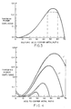
- To use the channel cell electrode for this purpose several test plating solutions would be used for plating within the channel cell electrode. All variables would be standardized except the ratio of acid to copper content in the test solutions. For each test solution, throwing power would be calculated by determining the ratio of the current passing through the edge or surface electrodes and the center electrodes as described above. The results would show a peak for throwing power for a given ratio.
- FIG. 3 of the drawings An exemplary plot of throwing power versus acid to copper ratio is shown in Figure 3 of the drawings for a copper plating solution containing 10 grams of copper sulfate pentahydrate per liter of solution.
- optimum results were obtained at an acid ratio varying between about 45:1 and 60:1.
- a ratio is selected that has a ratio varying from eighty percent of the peak to the peak ratio.
- the channel cell electrode may be used to monitor the performance and relative concentration of acid and copper of a plating solution during its use.
- the channel cell electrode would be suspended in the operating plating solution or solution would be continuously passed through the channel cell electrode at a remote location during plating. Current passing through the edge or surface electrodes and the center electrode would be continuously monitored and converted to a ratio depicting throwing power. If during the plating operation, there is variance from a predetermined value for throwing power, for example, as shown in Figure 3 of the drawings, corrections to the bath composition may be made to return the bath to its optimum operating composition.
- FIG. 1 This example better illustrates the use of the channel cell electrode depicted in Figures 1 and 2 of the drawings.
- the specific channel cell electrode used had two edge electrodes measuring 1/2 by 2 inches and a center electrode measuring 1/2 by 2 inches.
- the channel cell electrode was placed in a plating tank measuring 20 by 14 by 5.5 inches (length to height to width) with a total volume of 25 liters. Copper anodes were placed 9 inches from the center of the channel cell electrode.
- a cam gear was used to permit movement of the channel cell electrode perpendicular to the anodes over a distance of from 1 to 4 inches. This arrangement provided solution agitation.
- the plating tank was filled with a plating solution of the following composition: copper sulfate pentahydrate 10 gm/l sulfuric acid 150 gm/l chloride 50 ppm Deionized water to 1 liter
- the above bath corresponds to one having a hydrogen ion content (expressed as sulfuric acid) to copper metal content of 60 to 1 with a dissolved copper metal (cupric ion) content of 2.5 grams per liter of solution.
- the channel cell electrode Prior to use of the channel cell electrode, it is prepared by polishing with 600 mesh polish.
- the anodes are prepared by etching with a 30% nitric acid solution until they are of a matte pink coloration.
- the plating tank is filled with the plating solution and the anodes are immersed into the plating solution to a height whereby the plating solution is 2 inches above the bottom of the anodes.
- the two halves of the channel cell electrode are spaced 3/8 inches from each other replicating an aspect ratio of in excess of 50:1.
- a current of 6 amps was passed through the cell for test purposes, and the current on the edge electrodes and center electrodes of the channel cell electrode recorded.
- the ratio of the currents was found to be 0.30. This ratio is defined as throwing power. With sufficient data, the additional ratios can be obtained for the test solution and throwing power graphically depicted for all ratios for the test solution.
- Example 1 The procedure of Example 1 was repeated at three additional levels of dissolved copper, as shown in the following table. Acid concentration was varied for each example to give a series of acid to copper ratios for each test solution. Cu++ (gm/l)
- Example 2 15.0
- Example 3 12.5
- Example 4 5.0
- Example 5 2.5 For each example, throwing power as defined by the ratio of the current at the edges of the channel cell electrode to the current at the center electrode of the channel cell electrode, was determined for each acid to copper ratio.
- the above is illustrated by the plating of holes within a circuit board that is an epoxy copper clad circuit board base material that had been metallized by electroless metal deposition.
- the board contained holes having a 0.013 inch diameter and had a thickness (height) of 0.240 inches or an aspect ratio of 18.5 to 1.
- the board was electroplated using the plating bath of example 5 with an acid to copper metal ratio of 50:1. All holes were plated with copper of uniform thickness without visible signs of dogboning.
- Example 9 was repeated with a polyethylene oxide having a molecular weight of about 1,000,000 and was added to the solution in an amount of 1000 parts per million parts of solution.
- the results obtained are given in the following table: ratio - acid to copper Throwing Power with surfactant without surfactant 5 0.00 0.03 10 0.02 0.00 15 0.05 0.00 20 0.10 0.00 25 0.20 0.00 30 0.28 0.04 35 0.35 0.15 40 0.40 0.19 45 0.44 0.20 50 0.40 0.12
- the results are graphically represented in Figure 6 of the drawings. From the drawing, it can be seen that with the surfactant used, the throwing power was essentially doubled within the desired operating range.
Landscapes
- Engineering & Computer Science (AREA)
- Chemical & Material Sciences (AREA)
- Manufacturing & Machinery (AREA)
- Microelectronics & Electronic Packaging (AREA)
- Chemical Kinetics & Catalysis (AREA)
- Electrochemistry (AREA)
- Materials Engineering (AREA)
- Metallurgy (AREA)
- Organic Chemistry (AREA)
- Electroplating And Plating Baths Therefor (AREA)
- Printing Elements For Providing Electric Connections Between Printed Circuits (AREA)
Applications Claiming Priority (2)
| Application Number | Priority Date | Filing Date | Title |
|---|---|---|---|
| US07/235,051 US4897165A (en) | 1988-08-23 | 1988-08-23 | Electroplating composition and process for plating through holes in printed circuit boards |
| US235051 | 1988-08-23 |
Publications (2)
| Publication Number | Publication Date |
|---|---|
| EP0355804A2 true EP0355804A2 (de) | 1990-02-28 |
| EP0355804A3 EP0355804A3 (de) | 1991-07-17 |
Family
ID=22883891
Family Applications (1)
| Application Number | Title | Priority Date | Filing Date |
|---|---|---|---|
| EP19890115521 Withdrawn EP0355804A3 (de) | 1988-08-23 | 1989-08-23 | Elektroplattierungszusammensetzung und -verfahren |
Country Status (4)
| Country | Link |
|---|---|
| US (1) | US4897165A (de) |
| EP (1) | EP0355804A3 (de) |
| JP (1) | JPH02104690A (de) |
| KR (1) | KR900003419A (de) |
Cited By (2)
| Publication number | Priority date | Publication date | Assignee | Title |
|---|---|---|---|---|
| EP0440027A3 (en) * | 1990-01-29 | 1991-11-06 | Shipley Company Inc. | Additive for acid-copper electroplating baths to increase throwing power |
| EP1199383A3 (de) * | 2000-10-20 | 2004-02-11 | Shipley Company LLC | Bad zur reparierung einer Keimschicht |
Families Citing this family (14)
| Publication number | Priority date | Publication date | Assignee | Title |
|---|---|---|---|---|
| US5223118A (en) * | 1991-03-08 | 1993-06-29 | Shipley Company Inc. | Method for analyzing organic additives in an electroplating bath |
| US5376232A (en) * | 1993-08-23 | 1994-12-27 | Parlex Corporation | Method of manufacturing a printed circuit board |
| US5362534A (en) * | 1993-08-23 | 1994-11-08 | Parlex Corporation | Multiple layer printed circuit boards and method of manufacture |
| JP2001073182A (ja) * | 1999-07-15 | 2001-03-21 | Boc Group Inc:The | 改良された酸性銅電気メッキ用溶液 |
| JP2001089896A (ja) | 1999-09-20 | 2001-04-03 | Hitachi Ltd | めっき方法,めっき液,半導体装置及びその製造方法 |
| US20030030800A1 (en) * | 2001-07-15 | 2003-02-13 | Golden Josh H. | Method and system for the determination of arsenic in aqueous media |
| US20030049858A1 (en) * | 2001-07-15 | 2003-03-13 | Golden Josh H. | Method and system for analyte determination in metal plating baths |
| US20040046121A1 (en) * | 2001-07-15 | 2004-03-11 | Golden Josh H. | Method and system for analyte determination in metal plating baths |
| US20030049850A1 (en) * | 2001-09-12 | 2003-03-13 | Golden Josh H. | Enhanced detection of metal plating additives |
| US7144488B2 (en) * | 2002-06-05 | 2006-12-05 | Shipley Company, L.L.C. | Electrode, electrochemical cell, and method for analysis of electroplating baths |
| EP1475463B2 (de) * | 2002-12-20 | 2017-03-01 | Shipley Company, L.L.C. | Methode zum Elektroplattieren mit Umkehrpulsstrom |
| DE602005022650D1 (de) * | 2004-04-26 | 2010-09-16 | Rohm & Haas Elect Mat | Verbessertes Plattierungsverfahren |
| EP1741804B1 (de) * | 2005-07-08 | 2016-04-27 | Rohm and Haas Electronic Materials, L.L.C. | Procédé de dépôt électrolytique de cuivre |
| WO2020096906A1 (en) | 2018-11-07 | 2020-05-14 | Coventya, Inc. | Satin copper bath and method of depositing a satin copper layer |
Family Cites Families (6)
| Publication number | Priority date | Publication date | Assignee | Title |
|---|---|---|---|---|
| US3328273A (en) * | 1966-08-15 | 1967-06-27 | Udylite Corp | Electro-deposition of copper from acidic baths |
| US3562117A (en) * | 1967-09-18 | 1971-02-09 | Allied Chem | Method of copper electroplating printed circuit boards |
| US3769179A (en) * | 1972-01-19 | 1973-10-30 | Kewanee Oil Co | Copper plating process for printed circuits |
| US3770598A (en) * | 1972-01-21 | 1973-11-06 | Oxy Metal Finishing Corp | Electrodeposition of copper from acid baths |
| US4347108A (en) * | 1981-05-29 | 1982-08-31 | Rohco, Inc. | Electrodeposition of copper, acidic copper electroplating baths and additives therefor |
| US4673469A (en) * | 1984-06-08 | 1987-06-16 | Mcgean-Rohco, Inc. | Method of plating plastics |
-
1988
- 1988-08-23 US US07/235,051 patent/US4897165A/en not_active Expired - Lifetime
-
1989
- 1989-08-21 JP JP1214739A patent/JPH02104690A/ja active Pending
- 1989-08-22 KR KR1019890011922A patent/KR900003419A/ko not_active Withdrawn
- 1989-08-23 EP EP19890115521 patent/EP0355804A3/de not_active Withdrawn
Cited By (2)
| Publication number | Priority date | Publication date | Assignee | Title |
|---|---|---|---|---|
| EP0440027A3 (en) * | 1990-01-29 | 1991-11-06 | Shipley Company Inc. | Additive for acid-copper electroplating baths to increase throwing power |
| EP1199383A3 (de) * | 2000-10-20 | 2004-02-11 | Shipley Company LLC | Bad zur reparierung einer Keimschicht |
Also Published As
| Publication number | Publication date |
|---|---|
| US4897165A (en) | 1990-01-30 |
| JPH02104690A (ja) | 1990-04-17 |
| KR900003419A (ko) | 1990-03-26 |
| EP0355804A3 (de) | 1991-07-17 |
Similar Documents
| Publication | Publication Date | Title |
|---|---|---|
| US5068013A (en) | Electroplating composition and process | |
| US5051154A (en) | Additive for acid-copper electroplating baths to increase throwing power | |
| US4897165A (en) | Electroplating composition and process for plating through holes in printed circuit boards | |
| US5252196A (en) | Copper electroplating solutions and processes | |
| EP1475463B1 (de) | Methode zum Elektroplattieren mit Umkehrpulsstrom | |
| US4932518A (en) | Method and apparatus for determining throwing power of an electroplating solution | |
| GB2123036A (en) | Electroplating non-metallic surfaces | |
| US5004525A (en) | Copper electroplating composition | |
| EP2881389B1 (de) | Additive für galvanische Bäder | |
| US10435380B2 (en) | Metal plating compositions | |
| EP3288991B1 (de) | Reaktionsprodukte von diaminen mit reaktionsprodukten von monoaminen und bisanhydriden als additive für galvanikbäder | |
| US3562117A (en) | Method of copper electroplating printed circuit boards | |
| KR102125240B1 (ko) | 아민과 폴리아크릴아미드와 설톤의 반응 생성물의 화합물을 함유하는 구리 전기도금욕 | |
| JP2008506841A (ja) | 電流プロフィールの可変による銅メッキ硬度を制御するための電解メッキ方法 | |
| EP3359550B1 (de) | Kupfergalvanisierbäder mit verbindungen von reaktionsprodukten von aminen und chinonen | |
| KR102125234B1 (ko) | 아민과 폴리아크릴아미드의 반응 생성물의 화합물을 포함하는 구리 전기도금욕 | |
| US3859182A (en) | Coating printed circuit boards with tin or tin-lead alloy and tin-lead fluoborate plating baths | |
| JP6678220B2 (ja) | 電気めっき浴用の添加剤としてのビス無水物及びジアミンの反応生成物 |
Legal Events
| Date | Code | Title | Description |
|---|---|---|---|
| PUAI | Public reference made under article 153(3) epc to a published international application that has entered the european phase |
Free format text: ORIGINAL CODE: 0009012 |
|
| AK | Designated contracting states |
Kind code of ref document: A2 Designated state(s): DE FR GB IT NL |
|
| PUAL | Search report despatched |
Free format text: ORIGINAL CODE: 0009013 |
|
| AK | Designated contracting states |
Kind code of ref document: A3 Designated state(s): DE FR GB IT NL |
|
| 17P | Request for examination filed |
Effective date: 19911223 |
|
| 17Q | First examination report despatched |
Effective date: 19920427 |
|
| STAA | Information on the status of an ep patent application or granted ep patent |
Free format text: STATUS: THE APPLICATION IS DEEMED TO BE WITHDRAWN |
|
| 18D | Application deemed to be withdrawn |
Effective date: 19940503 |