EP0353492B1 - CMOS-Umsetzungsschaltung mit geringem Strom - Google Patents
CMOS-Umsetzungsschaltung mit geringem Strom Download PDFInfo
- Publication number
- EP0353492B1 EP0353492B1 EP89112588A EP89112588A EP0353492B1 EP 0353492 B1 EP0353492 B1 EP 0353492B1 EP 89112588 A EP89112588 A EP 89112588A EP 89112588 A EP89112588 A EP 89112588A EP 0353492 B1 EP0353492 B1 EP 0353492B1
- Authority
- EP
- European Patent Office
- Prior art keywords
- squaring
- low current
- current
- translator
- voltage
- Prior art date
- Legal status (The legal status is an assumption and is not a legal conclusion. Google has not performed a legal analysis and makes no representation as to the accuracy of the status listed.)
- Expired - Lifetime
Links
Images
Classifications
-
- H—ELECTRICITY
- H03—ELECTRONIC CIRCUITRY
- H03K—PULSE TECHNIQUE
- H03K19/00—Logic circuits, i.e. having at least two inputs acting on one output; Inverting circuits
- H03K19/0175—Coupling arrangements; Interface arrangements
- H03K19/0185—Coupling arrangements; Interface arrangements using field effect transistors only
- H03K19/018507—Interface arrangements
- H03K19/018521—Interface arrangements of complementary type, e.g. CMOS
-
- H—ELECTRICITY
- H03—ELECTRONIC CIRCUITRY
- H03K—PULSE TECHNIQUE
- H03K12/00—Producing pulses by distorting or combining sinusoidal waveforms
Definitions
- the present invention relates generally to complementary metal oxide semiconductor (CMOS) integrated circuits for low current, signal level translation applications. More particularly, the present invention is directed to translator circuit arrangements that are useful for providing a square wave output signal with preserved duty cycle, whether the input signal is a square wave or a sinusoid. These circuits are especially useful when translating a sinusoidal signal generated in a low current inverting stage.
- CMOS complementary metal oxide semiconductor
- Signal level translation is generally defined as a shifting of a given signal having a set peak-to-peak signal amplitude to another, different peak-to-peak signal amplitude.
- a square wave output signal is desired, even though the input signal may exist either as a square wave or as a sinewave.
- the square wave output signal is desirable for noise immunity and for interfacing with other digital circuitry that is commonly found in present-day radio and computer circuitry.
- One known type of translator relies upon an inverting stage, consisting of a complementary pair of devices, that is coupled to an input signal through a DC blocking capacitor.
- This inverting stage is supplied by a voltage source and includes a resistor coupled between output and input.
- Such a translator arrangement operates the two devices as a Class A stage and suffers from very high current consumption.
- the input voltage is several volts smaller than the supply voltage and consequently both devices will always be on and dissipate a large current.
- a low current inverting circuit as in the preamble of claim 1 is known from EP patent application no. EP-A-0255168 which discloses a CMOST input buffer for TTL level input signals.
- a low current translator for translating a square wave input signal having a first voltage range to a translated square wave output signal having a second voltage range while preserving a duty cycle associated with said input signal, comprising: at least one CMOS inverter for providing an output signal having the second voltage range which is an inverted and translated version of the square wave input signal having the first voltage range applied thereto; current supplying means for supplying substantially constant current to said at least one CMOS inverter at a supply node; and at least one capacitor means, connected at said supply node to said at least one CMOS inverter, as well as to said current supplying means, for storing and developing a supply voltage for said at least one CMOS inverter, said low current translator being characterised by: at least one voltage clamping stage, connected in parallel with said at least one CMOS inverter, and with said at least one capacitor means, as well as being connected to a second supply voltage for clamping the supply voltage for said at least one CMOS inverter to
- a squaring stage is coupled between the low current inverter and a low current translator that includes one or more inverting stages. This arrangement is able to achieve an output signal that maintains a precise duty cycle with low noise while drawing a very low current.
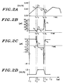
- Fig. 1 is a simplified schematic diagram of a low current inverter stage utilized to describe the present invention.
- Fig. 2 illustrates various current s and voltages generated at the identified points based upon input signal voltage Vin.
- Fig. 3 is a schematic diagram of a low current, direct coupled translator circuit in accordance with the present invention that is useful for translating a square wave from a first voltage range to a higher, second voltage range at the output.
- Fig. 4 is a schematic diagram of a low current squaring translator circuit in accordance with the present invention that is useful for squaring and then translating an internally generated sinusoidal signal to a square wave output signal while preserving an associated duty cycle thereof.
- Fig. 1 illustrates at 100 a simplified schematic diagram of a low current inverter utilized in an embodiment of the present invention.
- the inverter includes an inverting stage (102), a current supply (104), and a capacitor (106).
- the inverting stage (102) includes a pair of complementary metal-oxide-semiconductor (CMOS) devices (108, 109).
- CMOS complementary metal-oxide-semiconductor
- Device (108) is a P-channel device, while device (109) is an N-channel device.
- the output is taken from 110, and the input is applied to 112, as shown.
- the current supply (104) includes at least a constant current sink (or source) (114), and may include additional devices (116, 118) which act as a current mirror to ultimately feed supply node 105.
- the capacitor (106) includes a capacitor of about 5 picofarads (pF), as represented by C1 (labelled 120).
- This inverting stage (100) is useful either for voltage translation, or, as will be described later in conjunction with Fig. 4, as an inverting gain stage to drive a load while generating a sinusoidal signal when coupled to an external crystal (not shown in Fig. 1).
- Fig. 2 illustrates, at A,B,C,D, several currents and voltages developed at various identified points based upon a near rectangular input signal voltage, Vin.
- the circuit has three states it assumes during each cycle.
- the input signal is low and device 108 is ON, while device 109 is OFF.
- the voltage at node 110 is approximately equal to the value Vcap (represented by waveform A) which appears at node 105.
- the capacitor (106) is being charged, along with the load capacitance, CL, (121) by current source device (118), so that the voltage at supply node 105 is rising at a rate of approximately I/C1, where C1>>CL and I is the supply, or bias, current from the current supply (104).
- the third state occurs during the time period t4-t5.
- device 109 shuts OFF and device 108 turns fully ON, allowing a large instantaneous current to flow from C1 to charge the load capacitor.
- This can be seen by observing when the input signal (represented by wave form D) is switched low at input 112, device 108 sources a peak current IM3, (represented by waveform B) of about 90 microamperes (uA). Since the constant current source (104) only supplies about 10 microamperes, capacitor (106) supplies the excess current (represented by waveform C) needed to meet this peak requirement. As soon as the load capacitance is charged up to the value Vcap, the three-state cycle starts over again.
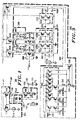
- Fig. 3 depicts a low current translator at 300 that includes one or more inverting stages (302).
- the inverting stages (302) are supplied from a current supply (304) and each stage is coupled to a respective one of a plurality of capacitors (306).
- Voltage clamping stages (308) are utilized to clamp the voltage developed on each of the capacitors (306) so that a predictable upper limit for each stage is established to preserve the duty cycle associated with the input signal.
- the voltage clamps (308) include a P-channel device (342A and 342B) to provide the upper limit on the voltage for each of stages 102A and 102B, respectively.
- the gate input of 342A is connected to a DC voltage which is approximately equal to the maximum value of the waveform applied to input port (318).
- Vsh′ can be approximately set to Vt.
- the inverting stages (302) include complementary pairs 312-313, 314-315. Although these two pairs are similar to stage 102 of Fig. 1, they have been labelled as 102A and 102B to indicate that they are being operated with I set slightly greater than lopt so that, regardless of input signal level variations and mismatch between stages, each one develops a level shift comparable to one P-channel threshold, Vt, equal to about 0.75 volts. Note in this example that stage 310 is acting as a buffer stage where the input signal at input port (318) has already been shifted at the output port (320) by 102A and 102B to within one P-channel threshold, Vt, of the output supply voltage.
- Current supply (304) is programmable (322) via control leads (324,326,328) to select an amount of current based upon an operating frequency range of 10-20 MHz and a variation in reference current of 1-2.6 »A.
- Node 330 is coupled to a reference voltage, Vref.
- the current is then mirrored via current mirrors (334,336,338,340A and 340B) having the multipliers shown, yielding 3-13.5Ua to 102A and 102B.
- High frequency voltage translation is accomplished at minimal current since the current required per stage is basically only that needed to charge a small load capacitance associated with minimally sized devices which are used in the inverting stages.
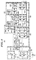
- Fig. 4 depicts a schematic diagram at 400 of a low current oscillator and translator arrangement that incorporates most aspects of the present invention when coupled to an external crystal (401).
- This arrangement includes a low current inverter (402), a squaring stage (404), and a low current translator (406).
- the low current inverter (402) includes a current source that is programmable (104′) for supplying an inverting gain stage (102) via a supply node (105) that has a capacitor (106) of about 15 pF, represented by capacitor 405.
- the squaring stage (404) includes a pair of squaring inverters (408, 410) and a supply buffer stage (412) that utilizes the voltage developed at node 105 for the low current inverter to bias the squaring inverters.
- the squaring inverters are made up of complementary pairs (414-415, and 416-417) that couple to the low current inverter at node 418 and to the low current translator at node 410. This stage generates a square wave that has fast rise and fall times prior to level shifting in the low current translator (406).
- the squaring inverters are DC coupled and biased class AB, the physical gate area and W/L ratio of the devices used in the squaring inverters can be made quite large to provide a large signal, low noise output at a very low current.
- the squaring stage (404) consumes 40 »A. Since the output has fast rise and fall times, it has a low sensitivity to noise and, therefore, minimally sized current efficient devices can be used in the following voltage translator stages.
- the physical size of the first squaring inverter is most important since its input signal level is significantly less that that of any of the following stages.
- the output of the first squaring inverter is not part of the resonant loop and, therefore, is not filtered, whereas the output of the low current inverter (402) is filtered.
- the W/L ratios for the P and N channel devices used in the first squaring inverter are 105/3 and 180/9, respectively.
- the supply buffer (412) has its output coupled to a capacitor (422) at a second supply node (424).
- Supply buffer 412 comprises a voltage follower, such as an operational amplifier connected as shown, that ensures that the voltage supplied to the squaring inverters is approximately the same as the voltage for the low current inverter.
- the low current translator (406) includes one or more translator stages (430,432) biased from a common source (434) that programs the current to the pairs of complementary devices represented at 102A and 102B.
- the voltage supply represented by 434 includes a programmable current source (440) and a load device (442) to develop the proper bias voltage at devices 444A and 444B to mirror the programmed current to translator stages 430 and 432.
- the capacitor (436A) is an integrated capacitance (445) of about 5 picofarads.
- the voltage clamp (438A) is shown as a P-channel device (446A) that utilizes the second supply voltage available at its input node 448 and establishes an upper limit voltage at its output node 450.
- translator stages such as stage 432 are coupled as shown, and include a device 444B to mirror the current programmed in 434 to inverting stage 102B, capacitor 436B, and voltage clamp 438B.
- Each of these stages is similar to translator stage 430, although the supply (434) will preferably be set to a current, I, slightly greater than lopt to allow for a range of input signal levels and for mismatch between stages to ensure a voltage shift of at least Vt per stage.
- translator stages (430, 432) incorporate three key design considerations to help preserve duty cycle, including;
- the low current CMOS translator, or level shifter is able to maintain a precise duty cycle output signal.
Landscapes
- Engineering & Computer Science (AREA)
- Computer Hardware Design (AREA)
- Physics & Mathematics (AREA)
- Computing Systems (AREA)
- General Engineering & Computer Science (AREA)
- Mathematical Physics (AREA)
- Manipulation Of Pulses (AREA)
- Logic Circuits (AREA)
- Dram (AREA)
Claims (9)
- Niedrigstrom-Umsetzer (300), der ein Rechteckwellen-Eingangssignal mit einem ersten Spannungsbereich in ein umgesetztes Rechteckwellen-Ausgangssignal mit einem zweiten Spannungsbereich unter Beibehaltung eines mit dem Eingangssignal verbundenen Impulsverhältnisses umsetzt und der umfaßt:
wenigstens einen CMOS-Inverter (120A), der ein Ausgangssignal mit dem zweiten Spannungsbereich erzeugt, das eine invertierte und umgesetzte Version des daran angelegten Rechteckwellen-Eingangssignals mit dem ersten Spannungsbereich darstellt;
eine Stromversorgungseinrichtung (304), die den wenigstens einen CMOS-Inverter (102A) an einem Versorgungsknoten mit einem im wesentlichen konstanten Strom versorgt; und
wenigstens eine Kondensatoreinrichtung (106A), die an dem Versorgungsknoten mit dem wenigstens einen CMOS-Inverter (102A) verbunden ist, sowie mit der Stromversorgungseinrichtung (304), die eine Versorgungsspannung für den wenigstens einen CMOS-Inverter speichert und erzeugt, wobei der Niedrigstrom-Umsetzer gekennzeichnet ist durch:
wenigstens eine Spannungsklemmschaltung (342A), die parallel mit dem wenigstens einen CMOS-Inverter (102A) und mit der wenigstens einen Kondensatoreinrichtung (106A) verbunden ist, und die ebenfalls an eine zweite Versorgungsspannung angeschlossen ist und die Versorgungsspannung für den wenigstens einen CMOS-Inverter auf eine obere Grenze beschränkt, wodurch das Ausgangssignal auf den zweiten Spannungsbereich beschränkt wird, der durch die zweite Versorgungsspannung begrenzt wird, um das mit dem Eingangssignal verbundene Impulsverhältnis beizubehalten. - Niedrigstrom-Umsetzer nach Anspruch 1, der umfaßt:
eine in Kaskade geschaltete Vielzahl von CMOS-Invertern (102A, 102B), die jeweils ein Ausgangssignal erzeugen, das eine invertierte und umgesetzte Version eines daran angelegten Eingangssignals darstellt; und
eine Vielzahl von Kondensatoreinrichtungen (106A, 106B), die jeweils mit einem entsprechenden der Vielzahl von CMOS-Invertern verbunden sind. - Niedrigstrom-Umsetzer nach Anspruch 1 oder 2, wobei die Stromversorgungseinrichtung eine programmierbare Stromquelle (304) umfaßt, die einen Strompegel zwischen 30 und 300 Mikroampere erzeugt, wobei sie eine Vielzahl von gleichgroßen programmierbaren Schritten nutzt, wenn sie bei 10-20 MHz arbeitet.
- Niedrigstrom-Rechteckformungs-Umsetzereinrichtung (400) zum Rechteckformen und anschließenden Umsetzen eines intern erzeugten sinusförmigen Signals, um ein umgesetztes Rechteckwellen-Ausgangssignal zu erzeugen, die umfaßt:
eine Niedrigstrom-Invertiereinrichtung (402), die eine Invertier-Verstärkungsstufe (102) umfaßt, die ein sinusförmiges Signal erzeugt, eine erste Stromversorgungseinrichtung (104′), die mit der Invertier-Verstärkungsstufe (102) und einer ersten Kondensatoreinrichtung (106) verbunden ist und an einem Knoten (105) eine erste Versorgungsspannung erzeugt;
Rechteckformungseinrichtung (404), die mit der Niedrigstrom-Invertiereinrichtung verbunden ist und einen ersten internen Versorgungsknoten (424) aufweist, der mit dem Knoten (105) verbunden ist und mit einer zweiten Kondensatoreinrichtung (422) verbunden ist, um die Rechteckformungseinrichtung mit der an dem Knoten (105) erzeugten Spannung zu versorgen, wobei die Rechteckformungseinrichtung (404) das sinusförmige Signal zu einem Rechteck formt, um ein Rechteckwellen-Signal zu erzeugen, das ein genaues Impulsverhältnis bei geringem Rauschen aufweist; und
einen Niedrigstrom-Umsetzer (406) nach Anspruch 1, 2 oder 3, der das Rechteckwellensignal, das ihm zugeführt wird, umsetzt und so ein umgesetztes Rechteckwellen-Ausgangssignal erzeugt, um ein genaues Impulsverhältnis bei geringem Rauschen beizubehalten. - Niedrigstrom-Rechteckformungs-Umsetzereinrichtung (400) nach Anspruch 4, wobei die Niedrigstrom-Invertiereinrichtung (402) mit einem Kristall (401) verbunden ist.
- Niedrigstrom-Rechteckformungs-Umsetzereinrichtung nach Anspruch 4 oder 5, wobei die erste Kondensatoreinrichtung (106) einen Kondensator (405) von 15 Pikofarad umfaßt.
- Niedrigstrom-Rechteckformungs-Umsetzereinrichtung nach Anspruch 4, 5 oder 6, wobei die erste Stromversorgungseinrichtung (104′) eine programmierbare Stromquelle (403) umfaßt.
- Niedrigstrom-Rechteckformungs-Umsetzereinrichtung nach Anspruch 4, wobei die Rechteckformungseinrichtung (404) umfaßt:
einen ersten Rechteckformungsinverter (408), der das sinusförmige Signal in Rechteckform bringt, um ein Zwischensignal zu erzeugen;
einen zweiten Rechteckformungsinverter (410), der mit dem ersten Rechteckformungsinverter verbunden ist und das Zwischensignal in Rechteckform bringt, um ein Rechteckwellen-Ausgangssignal zu erzeugen; und
eine Versorgungspuffereinrichtung (412), die mit den Knoten (105) der Niedrigstrom-Invertiereinrichtung verbunden ist und den ersten internen Versorgungsknoten (424) der Rechteckformungseinrichtung, der mit dem ersten und dem zweiten Rechteckformungsinverter verbunden ist, mit einer gepufferten Versorgungsspannung versorgt. - Niedrigstrom-Rechteckformungs-Umsetzereinrichtung nach Anspruch 8, wobei die Versorgungspuffereinrichtung einen Spannungsfolger (426) umfaßt.
Applications Claiming Priority (2)
| Application Number | Priority Date | Filing Date | Title |
|---|---|---|---|
| US07/227,589 US4982108A (en) | 1988-08-02 | 1988-08-02 | Low current CMOS translator circuit |
| US227589 | 1988-08-02 |
Publications (3)
| Publication Number | Publication Date |
|---|---|
| EP0353492A2 EP0353492A2 (de) | 1990-02-07 |
| EP0353492A3 EP0353492A3 (en) | 1990-05-23 |
| EP0353492B1 true EP0353492B1 (de) | 1995-04-05 |
Family
ID=22853699
Family Applications (1)
| Application Number | Title | Priority Date | Filing Date |
|---|---|---|---|
| EP89112588A Expired - Lifetime EP0353492B1 (de) | 1988-08-02 | 1989-07-10 | CMOS-Umsetzungsschaltung mit geringem Strom |
Country Status (8)
| Country | Link |
|---|---|
| US (1) | US4982108A (de) |
| EP (1) | EP0353492B1 (de) |
| AT (1) | ATE120907T1 (de) |
| CA (1) | CA1304138C (de) |
| DE (1) | DE68922036T2 (de) |
| IE (1) | IE67869B1 (de) |
| MX (1) | MX167546B (de) |
| WO (1) | WO1990001833A1 (de) |
Families Citing this family (6)
| Publication number | Priority date | Publication date | Assignee | Title |
|---|---|---|---|---|
| JPH04297118A (ja) * | 1991-01-21 | 1992-10-21 | Fujitsu Ltd | パルス発生回路及びパルス発生回路を備える半導体装置 |
| US5343094A (en) * | 1993-01-13 | 1994-08-30 | National Semiconductor Corporation | Low noise logic amplifier with nondifferential to differential conversion |
| US5559941A (en) * | 1994-10-26 | 1996-09-24 | Brechner; Eric L. | Method for smoothly maintaining a vertical orientation during computer animation |
| US9178554B2 (en) | 2014-03-28 | 2015-11-03 | Futurewei Technologies, Inc. | Phase correction apparatus and method |
| US12469436B2 (en) | 2023-07-27 | 2025-11-11 | Google Llc | Memory cell for a pixel of a display |
| WO2025024423A1 (en) * | 2023-07-27 | 2025-01-30 | Google Llc | Memory cell for a pixel of a display |
Family Cites Families (14)
| Publication number | Priority date | Publication date | Assignee | Title |
|---|---|---|---|---|
| US3801831A (en) * | 1972-10-13 | 1974-04-02 | Motorola Inc | Voltage level shifting circuit |
| US3922596A (en) * | 1973-08-13 | 1975-11-25 | Motorola Inc | Current regulator |
| US3855549A (en) * | 1973-08-24 | 1974-12-17 | Rca Corp | Circuit, such as cmos crystal oscillator, with reduced power consumption |
| DE3072118D1 (en) * | 1979-12-26 | 1988-09-22 | Toshiba Kk | A driver circuit for charge coupled device |
| US4390802A (en) * | 1980-12-22 | 1983-06-28 | Motorola, Inc. | Low-voltage, high-noise immunity I2 L interface |
| US4591807A (en) * | 1984-12-03 | 1986-05-27 | Motorola, Inc. | Low power, low voltage oscillator |
| US4587497A (en) * | 1984-12-24 | 1986-05-06 | Motorola, Inc. | Low-power low-harmonic transistor oscillator |
| JPS62159917A (ja) * | 1986-01-08 | 1987-07-15 | Toshiba Corp | 集積回路におけるインバ−タ回路 |
| US4710724A (en) * | 1986-04-02 | 1987-12-01 | Motorola, Inc. | Differential CMOS comparator for switched capacitor applications |
| NL8601953A (nl) * | 1986-07-30 | 1988-02-16 | Philips Nv | Cmost-ingangsbuffer voor ttl-niveau ingangssignalen. |
| US4716319A (en) * | 1986-08-04 | 1987-12-29 | Motorola, Inc. | Switched capacitor filter for low voltage applications |
| US4783603A (en) * | 1987-01-08 | 1988-11-08 | Cypress Semiconductor Corporation | TTL to MOS converter with power supply noise rejection |
| US4710730A (en) * | 1987-03-20 | 1987-12-01 | Motorola, Inc. | Data clock oscillator having accurate duty cycle |
| US4752703A (en) * | 1987-04-23 | 1988-06-21 | Industrial Technology Research Institute | Current source polarity switching circuit |
-
1988
- 1988-08-02 US US07/227,589 patent/US4982108A/en not_active Expired - Fee Related
-
1989
- 1989-06-05 CA CA000601700A patent/CA1304138C/en not_active Expired - Lifetime
- 1989-06-15 IE IE193589A patent/IE67869B1/en not_active IP Right Cessation
- 1989-06-16 WO PCT/US1989/002630 patent/WO1990001833A1/en not_active Ceased
- 1989-07-07 MX MX016721A patent/MX167546B/es unknown
- 1989-07-10 DE DE68922036T patent/DE68922036T2/de not_active Expired - Fee Related
- 1989-07-10 AT AT89112588T patent/ATE120907T1/de not_active IP Right Cessation
- 1989-07-10 EP EP89112588A patent/EP0353492B1/de not_active Expired - Lifetime
Non-Patent Citations (3)
| Title |
|---|
| HOROWITZ and HILL, "The Art of Electronics", 1980, Cambridge University Press, Cambridge, US, pages 176, 182 and 183 * |
| PATENT ABSTRACTS OF JAPAN, vol. 10, no. 95 (E-395) (2152), 12 April 1986 & JP-A-60 237 724 * |
| PATENT ABSTRACTS OF JAPAN, vol. 8, no. 213 (E-269)(1650), 28 September 1984 & JP-A-59 99 817 * |
Also Published As
| Publication number | Publication date |
|---|---|
| IE891935L (en) | 1990-02-02 |
| CA1304138C (en) | 1992-06-23 |
| DE68922036D1 (de) | 1995-05-11 |
| ATE120907T1 (de) | 1995-04-15 |
| IE67869B1 (en) | 1996-05-01 |
| EP0353492A2 (de) | 1990-02-07 |
| US4982108A (en) | 1991-01-01 |
| MX167546B (es) | 1993-03-29 |
| EP0353492A3 (en) | 1990-05-23 |
| DE68922036T2 (de) | 1995-10-26 |
| WO1990001833A1 (en) | 1990-02-22 |
Similar Documents
| Publication | Publication Date | Title |
|---|---|---|
| CA1206535A (en) | Interface circuit | |
| EP0621694B1 (de) | Schnittstellenschaltung mit niedrigem Verbrauch | |
| US6040729A (en) | Digital output buffer for multiple voltage system | |
| US5140179A (en) | Master-slave type flip-flop circuit | |
| EP0608489A2 (de) | Niedrig-nach Hochpegel Umsetzer mit latch-up-Festigkeit | |
| US4437024A (en) | Actively controlled input buffer | |
| JPH05145384A (ja) | Cmosレシーバ入力インターフエース回路 | |
| US20110037500A1 (en) | Integrated circuit comparator or amplifier | |
| US6441663B1 (en) | SOI CMOS Schmitt trigger circuits with controllable hysteresis | |
| US4461963A (en) | MOS Power-on reset circuit | |
| EP0239762B1 (de) | Pufferschaltung | |
| US20020149400A1 (en) | Low voltage differential to single-ended converter | |
| EP0482942A2 (de) | Dreizustands-Präzisionsausgangstreiber mit einer Spannungsklemmcharakteristik | |
| US6650167B1 (en) | Multi-level/single ended input level shifter circuit | |
| US4406957A (en) | Input buffer circuit | |
| EP0353492B1 (de) | CMOS-Umsetzungsschaltung mit geringem Strom | |
| US5646551A (en) | Mixed mode output buffer circuit for CMOSIC | |
| EP0501085A1 (de) | Pegelschieberschaltung für schnelle leistungsarme ECL nach CMOS-Eingangspuffern in biCMOS-Technik | |
| US4578601A (en) | High speed TTL clock input buffer circuit which minimizes power and provides CMOS level translation | |
| JP3492765B2 (ja) | レベル変換回路 | |
| EP0622903A2 (de) | Eingangstreiberschaltung mit Schlafmodus und Bus-Haltefunktion | |
| US4897567A (en) | Fast level translator circuit | |
| US6043683A (en) | Output pad circuit using control signal | |
| EP0339165A1 (de) | GaAs-Mesfet-Logik-Schaltungen mit Gegentakt-Ausgangspufferschaltungen | |
| US4958132A (en) | Complementary metal-oxide-semiconductor translator |
Legal Events
| Date | Code | Title | Description |
|---|---|---|---|
| PUAI | Public reference made under article 153(3) epc to a published international application that has entered the european phase |
Free format text: ORIGINAL CODE: 0009012 |
|
| AK | Designated contracting states |
Kind code of ref document: A2 Designated state(s): AT BE CH DE FR GB IT LI LU NL SE |
|
| PUAL | Search report despatched |
Free format text: ORIGINAL CODE: 0009013 |
|
| AK | Designated contracting states |
Kind code of ref document: A3 Designated state(s): AT BE CH DE FR GB IT LI LU NL SE |
|
| 17P | Request for examination filed |
Effective date: 19900628 |
|
| 17Q | First examination report despatched |
Effective date: 19910725 |
|
| GRAA | (expected) grant |
Free format text: ORIGINAL CODE: 0009210 |
|
| ITF | It: translation for a ep patent filed | ||
| AK | Designated contracting states |
Kind code of ref document: B1 Designated state(s): AT BE CH DE FR GB IT LI LU NL SE |
|
| REF | Corresponds to: |
Ref document number: 120907 Country of ref document: AT Date of ref document: 19950415 Kind code of ref document: T |
|
| ET | Fr: translation filed | ||
| REF | Corresponds to: |
Ref document number: 68922036 Country of ref document: DE Date of ref document: 19950511 |
|
| PLBE | No opposition filed within time limit |
Free format text: ORIGINAL CODE: 0009261 |
|
| STAA | Information on the status of an ep patent application or granted ep patent |
Free format text: STATUS: NO OPPOSITION FILED WITHIN TIME LIMIT |
|
| 26N | No opposition filed | ||
| REG | Reference to a national code |
Ref country code: CH Ref legal event code: PUE Owner name: MOTOROLA, INC. TRANSFER- CTS CORPORATION |
|
| NLS | Nl: assignments of ep-patents |
Owner name: CTS CORPORATION |
|
| REG | Reference to a national code |
Ref country code: FR Ref legal event code: TP |
|
| REG | Reference to a national code |
Ref country code: GB Ref legal event code: 732E |
|
| PGFP | Annual fee paid to national office [announced via postgrant information from national office to epo] |
Ref country code: FR Payment date: 20010619 Year of fee payment: 13 |
|
| PGFP | Annual fee paid to national office [announced via postgrant information from national office to epo] |
Ref country code: SE Payment date: 20010620 Year of fee payment: 13 Ref country code: DE Payment date: 20010620 Year of fee payment: 13 |
|
| PGFP | Annual fee paid to national office [announced via postgrant information from national office to epo] |
Ref country code: NL Payment date: 20010621 Year of fee payment: 13 Ref country code: GB Payment date: 20010621 Year of fee payment: 13 Ref country code: CH Payment date: 20010621 Year of fee payment: 13 Ref country code: AT Payment date: 20010621 Year of fee payment: 13 |
|
| PGFP | Annual fee paid to national office [announced via postgrant information from national office to epo] |
Ref country code: LU Payment date: 20010629 Year of fee payment: 13 |
|
| PGFP | Annual fee paid to national office [announced via postgrant information from national office to epo] |
Ref country code: BE Payment date: 20010713 Year of fee payment: 13 |
|
| REG | Reference to a national code |
Ref country code: GB Ref legal event code: IF02 |
|
| PG25 | Lapsed in a contracting state [announced via postgrant information from national office to epo] |
Ref country code: LU Free format text: LAPSE BECAUSE OF NON-PAYMENT OF DUE FEES Effective date: 20020710 Ref country code: GB Free format text: LAPSE BECAUSE OF NON-PAYMENT OF DUE FEES Effective date: 20020710 Ref country code: AT Free format text: LAPSE BECAUSE OF NON-PAYMENT OF DUE FEES Effective date: 20020710 |
|
| PG25 | Lapsed in a contracting state [announced via postgrant information from national office to epo] |
Ref country code: SE Free format text: LAPSE BECAUSE OF NON-PAYMENT OF DUE FEES Effective date: 20020711 |
|
| PG25 | Lapsed in a contracting state [announced via postgrant information from national office to epo] |
Ref country code: LI Free format text: LAPSE BECAUSE OF NON-PAYMENT OF DUE FEES Effective date: 20020731 Ref country code: CH Free format text: LAPSE BECAUSE OF NON-PAYMENT OF DUE FEES Effective date: 20020731 Ref country code: BE Free format text: LAPSE BECAUSE OF NON-PAYMENT OF DUE FEES Effective date: 20020731 |
|
| BERE | Be: lapsed |
Owner name: *CTS CORP. Effective date: 20020731 |
|
| PG25 | Lapsed in a contracting state [announced via postgrant information from national office to epo] |
Ref country code: NL Free format text: LAPSE BECAUSE OF NON-PAYMENT OF DUE FEES Effective date: 20030201 Ref country code: DE Free format text: LAPSE BECAUSE OF NON-PAYMENT OF DUE FEES Effective date: 20030201 |
|
| EUG | Se: european patent has lapsed | ||
| GBPC | Gb: european patent ceased through non-payment of renewal fee |
Effective date: 20020710 |
|
| REG | Reference to a national code |
Ref country code: CH Ref legal event code: PL |
|
| PG25 | Lapsed in a contracting state [announced via postgrant information from national office to epo] |
Ref country code: FR Free format text: LAPSE BECAUSE OF NON-PAYMENT OF DUE FEES Effective date: 20030331 |
|
| NLV4 | Nl: lapsed or anulled due to non-payment of the annual fee |
Effective date: 20030201 |
|
| REG | Reference to a national code |
Ref country code: FR Ref legal event code: ST |
|
| PG25 | Lapsed in a contracting state [announced via postgrant information from national office to epo] |
Ref country code: IT Free format text: LAPSE BECAUSE OF NON-PAYMENT OF DUE FEES;WARNING: LAPSES OF ITALIAN PATENTS WITH EFFECTIVE DATE BEFORE 2007 MAY HAVE OCCURRED AT ANY TIME BEFORE 2007. THE CORRECT EFFECTIVE DATE MAY BE DIFFERENT FROM THE ONE RECORDED. Effective date: 20050710 |