EP0348026A1 - Diamond growth on a substrate using microwave energy - Google Patents
Diamond growth on a substrate using microwave energy Download PDFInfo
- Publication number
- EP0348026A1 EP0348026A1 EP89304200A EP89304200A EP0348026A1 EP 0348026 A1 EP0348026 A1 EP 0348026A1 EP 89304200 A EP89304200 A EP 89304200A EP 89304200 A EP89304200 A EP 89304200A EP 0348026 A1 EP0348026 A1 EP 0348026A1
- Authority
- EP
- European Patent Office
- Prior art keywords
- substrate
- diamond
- nitride
- microwave energy
- crystalline
- Prior art date
- Legal status (The legal status is an assumption and is not a legal conclusion. Google has not performed a legal analysis and makes no representation as to the accuracy of the status listed.)
- Granted
Links
- 239000010432 diamond Substances 0.000 title claims abstract description 64
- 229910003460 diamond Inorganic materials 0.000 title claims abstract description 61
- 239000000758 substrate Substances 0.000 title claims abstract description 44
- 150000004767 nitrides Chemical class 0.000 claims abstract description 22
- 150000001722 carbon compounds Chemical class 0.000 claims abstract description 20
- OKTJSMMVPCPJKN-UHFFFAOYSA-N Carbon Chemical compound [C] OKTJSMMVPCPJKN-UHFFFAOYSA-N 0.000 claims abstract description 12
- 229910002804 graphite Inorganic materials 0.000 claims abstract description 7
- 239000010439 graphite Substances 0.000 claims abstract description 7
- 229910052799 carbon Inorganic materials 0.000 claims abstract description 5
- 150000001875 compounds Chemical class 0.000 claims abstract description 5
- 238000000034 method Methods 0.000 claims description 34
- VNWKTOKETHGBQD-UHFFFAOYSA-N methane Chemical compound C VNWKTOKETHGBQD-UHFFFAOYSA-N 0.000 claims description 8
- 229910052581 Si3N4 Inorganic materials 0.000 claims description 6
- HQVNEWCFYHHQES-UHFFFAOYSA-N silicon nitride Chemical group N12[Si]34N5[Si]62N3[Si]51N64 HQVNEWCFYHHQES-UHFFFAOYSA-N 0.000 claims description 6
- 239000007789 gas Substances 0.000 claims description 5
- 229930195733 hydrocarbon Natural products 0.000 claims description 5
- 150000002430 hydrocarbons Chemical class 0.000 claims description 5
- 239000001257 hydrogen Substances 0.000 claims description 5
- 229910052739 hydrogen Inorganic materials 0.000 claims description 5
- UFHFLCQGNIYNRP-UHFFFAOYSA-N Hydrogen Chemical compound [H][H] UFHFLCQGNIYNRP-UHFFFAOYSA-N 0.000 claims description 4
- 239000000203 mixture Substances 0.000 claims description 4
- 239000004215 Carbon black (E152) Substances 0.000 claims description 3
- 229910017083 AlN Inorganic materials 0.000 claims description 2
- PIGFYZPCRLYGLF-UHFFFAOYSA-N Aluminum nitride Chemical compound [Al]#N PIGFYZPCRLYGLF-UHFFFAOYSA-N 0.000 claims description 2
- NRTOMJZYCJJWKI-UHFFFAOYSA-N Titanium nitride Chemical compound [Ti]#N NRTOMJZYCJJWKI-UHFFFAOYSA-N 0.000 claims description 2
- 238000000354 decomposition reaction Methods 0.000 claims description 2
- 230000008021 deposition Effects 0.000 claims description 2
- 239000011521 glass Substances 0.000 claims description 2
- 229910052751 metal Inorganic materials 0.000 claims description 2
- 239000002184 metal Substances 0.000 claims description 2
- MZLGASXMSKOWSE-UHFFFAOYSA-N tantalum nitride Chemical compound [Ta]#N MZLGASXMSKOWSE-UHFFFAOYSA-N 0.000 claims description 2
- 239000013078 crystal Substances 0.000 description 8
- IJGRMHOSHXDMSA-UHFFFAOYSA-N Atomic nitrogen Chemical compound N#N IJGRMHOSHXDMSA-UHFFFAOYSA-N 0.000 description 6
- XUIMIQQOPSSXEZ-UHFFFAOYSA-N Silicon Chemical compound [Si] XUIMIQQOPSSXEZ-UHFFFAOYSA-N 0.000 description 5
- 229910052710 silicon Inorganic materials 0.000 description 5
- 239000010703 silicon Substances 0.000 description 5
- 238000005229 chemical vapour deposition Methods 0.000 description 3
- 229910052757 nitrogen Inorganic materials 0.000 description 3
- CSCPPACGZOOCGX-UHFFFAOYSA-N Acetone Chemical compound CC(C)=O CSCPPACGZOOCGX-UHFFFAOYSA-N 0.000 description 2
- CURLTUGMZLYLDI-UHFFFAOYSA-N Carbon dioxide Chemical compound O=C=O CURLTUGMZLYLDI-UHFFFAOYSA-N 0.000 description 2
- UGFAIRIUMAVXCW-UHFFFAOYSA-N Carbon monoxide Chemical compound [O+]#[C-] UGFAIRIUMAVXCW-UHFFFAOYSA-N 0.000 description 2
- ATUOYWHBWRKTHZ-UHFFFAOYSA-N Propane Chemical compound CCC ATUOYWHBWRKTHZ-UHFFFAOYSA-N 0.000 description 2
- 229910002091 carbon monoxide Inorganic materials 0.000 description 2
- 230000001747 exhibiting effect Effects 0.000 description 2
- 150000002431 hydrogen Chemical class 0.000 description 2
- 239000000463 material Substances 0.000 description 2
- 229910052582 BN Inorganic materials 0.000 description 1
- PZNSFCLAULLKQX-UHFFFAOYSA-N Boron nitride Chemical compound N#B PZNSFCLAULLKQX-UHFFFAOYSA-N 0.000 description 1
- OTMSDBZUPAUEDD-UHFFFAOYSA-N Ethane Chemical compound CC OTMSDBZUPAUEDD-UHFFFAOYSA-N 0.000 description 1
- LFQSCWFLJHTTHZ-UHFFFAOYSA-N Ethanol Chemical compound CCO LFQSCWFLJHTTHZ-UHFFFAOYSA-N 0.000 description 1
- XPDWGBQVDMORPB-UHFFFAOYSA-N Fluoroform Chemical compound FC(F)F XPDWGBQVDMORPB-UHFFFAOYSA-N 0.000 description 1
- 229910004205 SiNX Inorganic materials 0.000 description 1
- PNEYBMLMFCGWSK-UHFFFAOYSA-N aluminium oxide Inorganic materials [O-2].[O-2].[O-2].[Al+3].[Al+3] PNEYBMLMFCGWSK-UHFFFAOYSA-N 0.000 description 1
- 230000015572 biosynthetic process Effects 0.000 description 1
- 229910002092 carbon dioxide Inorganic materials 0.000 description 1
- 239000001569 carbon dioxide Substances 0.000 description 1
- 239000000919 ceramic Substances 0.000 description 1
- 239000002178 crystalline material Substances 0.000 description 1
- 238000000151 deposition Methods 0.000 description 1
- 239000008246 gaseous mixture Substances 0.000 description 1
- 239000010437 gem Substances 0.000 description 1
- 229910001751 gemstone Inorganic materials 0.000 description 1
- 238000010438 heat treatment Methods 0.000 description 1
- WMIYKQLTONQJES-UHFFFAOYSA-N hexafluoroethane Chemical compound FC(F)(F)C(F)(F)F WMIYKQLTONQJES-UHFFFAOYSA-N 0.000 description 1
- 239000007788 liquid Substances 0.000 description 1
- 238000004519 manufacturing process Methods 0.000 description 1
- 125000004433 nitrogen atom Chemical group N* 0.000 description 1
- 239000002245 particle Substances 0.000 description 1
- 239000001294 propane Substances 0.000 description 1
- 239000010453 quartz Substances 0.000 description 1
- VYPSYNLAJGMNEJ-UHFFFAOYSA-N silicon dioxide Inorganic materials O=[Si]=O VYPSYNLAJGMNEJ-UHFFFAOYSA-N 0.000 description 1
- 238000003786 synthesis reaction Methods 0.000 description 1
- TXEYQDLBPFQVAA-UHFFFAOYSA-N tetrafluoromethane Chemical compound FC(F)(F)F TXEYQDLBPFQVAA-UHFFFAOYSA-N 0.000 description 1
- 235000012431 wafers Nutrition 0.000 description 1
Images


Classifications
-
- C—CHEMISTRY; METALLURGY
- C30—CRYSTAL GROWTH
- C30B—SINGLE-CRYSTAL GROWTH; UNIDIRECTIONAL SOLIDIFICATION OF EUTECTIC MATERIAL OR UNIDIRECTIONAL DEMIXING OF EUTECTOID MATERIAL; REFINING BY ZONE-MELTING OF MATERIAL; PRODUCTION OF A HOMOGENEOUS POLYCRYSTALLINE MATERIAL WITH DEFINED STRUCTURE; SINGLE CRYSTALS OR HOMOGENEOUS POLYCRYSTALLINE MATERIAL WITH DEFINED STRUCTURE; AFTER-TREATMENT OF SINGLE CRYSTALS OR A HOMOGENEOUS POLYCRYSTALLINE MATERIAL WITH DEFINED STRUCTURE; APPARATUS THEREFOR
- C30B25/00—Single-crystal growth by chemical reaction of reactive gases, e.g. chemical vapour-deposition growth
- C30B25/02—Epitaxial-layer growth
- C30B25/10—Heating of the reaction chamber or the substrate
- C30B25/105—Heating of the reaction chamber or the substrate by irradiation or electric discharge
-
- C—CHEMISTRY; METALLURGY
- C30—CRYSTAL GROWTH
- C30B—SINGLE-CRYSTAL GROWTH; UNIDIRECTIONAL SOLIDIFICATION OF EUTECTIC MATERIAL OR UNIDIRECTIONAL DEMIXING OF EUTECTOID MATERIAL; REFINING BY ZONE-MELTING OF MATERIAL; PRODUCTION OF A HOMOGENEOUS POLYCRYSTALLINE MATERIAL WITH DEFINED STRUCTURE; SINGLE CRYSTALS OR HOMOGENEOUS POLYCRYSTALLINE MATERIAL WITH DEFINED STRUCTURE; AFTER-TREATMENT OF SINGLE CRYSTALS OR A HOMOGENEOUS POLYCRYSTALLINE MATERIAL WITH DEFINED STRUCTURE; APPARATUS THEREFOR
- C30B29/00—Single crystals or homogeneous polycrystalline material with defined structure characterised by the material or by their shape
- C30B29/02—Elements
- C30B29/04—Diamond
Definitions
- This invention relates to diamond growth.
- a method of growing crystalline diamond on a substrate including the steps of providing a surface of a suitable nitride, placing the substrate on the nitride surface, creating an atmosphere of a gaseous carbon compound around the substrate, bringing the temperature of the nitride surface and the substrate to at least 600°C, and subjecting the gaseous carbon compound to microwave energy suitable to cause the compound to decompose and produce carbon which deposits, on the substrate and forms crystalline diamond thereon.
- the substrate is placed on a surface of a suitable nitride.
- This nitride releases nitrogen atoms in small amounts which create a suitable nitrogen concentration in the atmosphere surrounding the substrate slowing the diamond growth and hence improving it.
- This surface will generally and preferably cover completely a support which is preferably a microwave energy sink, i.e. a support which will absorb microwave energy and thereby be heated.
- a support is a graphite support which will absorb at least 50% of the microwave energy.
- the nitride may be silicon nitride, aluminium nitride, titanium nitride, tantalum nitride or the like.
- the nitride surface will typically be formed on a support by means of known chemical vapour deposition methods. Such methods will result in the nitride containing substantial quantities of hydrogen, e.g. 1 to 30 atomic percent. This hydrogen will be strongly bonded.
- the temperature of the nitride surface and the substrate are preferably maintained at a temperature of 600 to 1000°C during the time the decomposition of the carbon compound and deposition of carbon on the substrate take place.
- the substrate will generally be at a higher temperature than the nitride surface.
- the microwave energy which is used to decompose the carbon compound will typically be the source of the heating energy for the surface.
- the frequency of the microwave energy may vary over a wide range. Typically the frequency will be in the range 200 MHz to 90 GHz. An example of a typical frequency which may be used is 2,45 GHz.
- the microwave energy will typically be maintained for a period of at least several hours, e.g. 2 to 10 hours.
- the gaseous carbon compound will preferably be introduced into a confined space containing the substrate.
- the compound may take the form of a mixture with a reducing gas such as hydrogen. Typically, the mixture will contain less than 5% by volume of the carbon compound.
- the carbon compound will generally be a suitable hydrocarbon such as methane. Examples of other suitable carbon compounds are ethane, propane, fluorinated hydrocarbons such as CF4, C2F6 and CHF3, carbon monoxide and carbon dioxide.
- the substrate may be crystalline, glassy or amorphous.
- suitable substrates are glass, metal, ceramics and diamond. If the substrate is diamond or a cubic crystalline material of a suitable lattice constant match to diamond, epitaxial diamond growth will occur thereon. Good crystalline diamond layers and crystals have been grown on silicon substrates using the method of the invention.
- the substrate is diamond and the invention allows for the production of crystalline diamond layers of good quality to be grown thereon.
- the diamond substrate may be natural or synthetic.
- the substrate may be a diamond of type Ia and it is possible to grow diamond of type IIa thereon.
- Diamond of type Ia contains aggregated nitrogen and constitutes 98% of all natural diamond, while diamond of type IIa is nitrogen free and has the best thermal conductivity of any known material.
- a diamond body of type Ia having diamond of type IIa joined thereto can be used as a heat sink.
- a diamond body comprising a layer of diamond of type IIa joined to a diamond substrate is believed to be new and forms another aspect of the invention. Since the growth of the diamond of type IIa will be epitaxial, the diamond layer and the substrate will be joined by an integrally formed diamond interface.
- the method of the invention it is possible by the method of the invention not only to grow diamond films but also large diamond crystals. Indeed, it is possible to produce excellent cubo-octahedral diamond crystals and thick epitaxial crystalline diamond films. Because of the high quality crystalline diamond which is grown, it is possible to use the method of the invention to grow diamond in cracks in naturally occurring gem-stone quality diamonds to improve their quality.
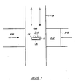
- FIG. 1 illustrates schematically apparatus suitable for carrying out the method of the invention.
- the apparatus consists of a quartz tube 10 in which is suspended one or more graphite boats 12.
- One graphite boat is illustrated and it has a layer 14 of silicon nitride covering its entire surface 16. The graphite boat is thus completely enclosed by the nitride layer.
- Microwave energy from a suitable source passes into the space 18 within the tube through the passage 20.
- a quarter wavelength shorting plate 22 for the microwaves is provided in passage 24.
- a source of gaseous carbon compound is fed into the space 18 in the direction of the arrow A.
- This apparatus was used to produce crystalline diamond growth on various diamond or cubic boron nitride (CBN) seed crystals 26 which were located on the silicon nitride layer 14.
- the wavelength of the microwaves was 2,45 GHz
- the temperature of the graphite boat was maintained at a temperature of about 730°C and that of the seed crystals was maintained at 830°C.
- the gaseous carbon compound consisted of methane gas which constituted about 5% by volume of a mixture with hydrogen gas.
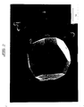
- Figures 2 to 6 illustrate examples of diamonds and diamond films produced by the method of the invention.
- Figure 2 is a photograph of a diamond crystal about 2 to 3 microns in size which was grown on a silicon substrate without the use of any diamond seed.
- Figure 3 is a photograph of twinned diamond particles grown on a silicon substrate with CBN seeds.
- Figures 4 and 5 are different photographs of the same continuous diamond film exhibiting (100) and (111) facets.
- Figure 6 is a photograph of a diamond film grown on a silicon substrate exhibiting only (100) facets.
Abstract
Description
- This invention relates to diamond growth.
- Various methods have been proposed and tried for growing diamond on diamond seed crystals by chemical vapour deposition (CVD) using gaseous carbon compounds such as hydrocarbons or carbon monoxide. The gaseous compound can be produced from a liquid carbon compound such as an alcohol or acetone. The gaseous carbon compounds may be decomposed by various methods including the use of heat and radio frequency (RF) energy, and also by means of microwave energy. Much of the material which is grown by these prior art methods is diamond-like rather than crystalline diamond.
- An article entitled "Diamond Synthesis from Gas Phase in Microwave Plasma" by M. Kamo et al, Journal of Crystal Growth 62 (1983) 642 to 644 describes preliminary results of a study involving crystalline diamond growth on a non-diamond substrate using a gaseous mixture of hydrogen and methane under microwave glow discharge conditions. The diamond growth took place on silicon wafers supported by an alumina basket.
- According to the present invention, there is provided a method of growing crystalline diamond on a substrate including the steps of providing a surface of a suitable nitride, placing the substrate on the nitride surface, creating an atmosphere of a gaseous carbon compound around the substrate, bringing the temperature of the nitride surface and the substrate to at least 600°C, and subjecting the gaseous carbon compound to microwave energy suitable to cause the compound to decompose and produce carbon which deposits, on the substrate and forms crystalline diamond thereon.
-
- Figure 1 illustrates schematically apparatus suitable for carrying out the method of the invention; and
- Figures 2 to 6 are photographs of typical diamonds and diamond films produced by the method of the invention;
- Essential to the invention is that the substrate is placed on a surface of a suitable nitride. This nitride, during the method, releases nitrogen atoms in small amounts which create a suitable nitrogen concentration in the atmosphere surrounding the substrate slowing the diamond growth and hence improving it. This surface will generally and preferably cover completely a support which is preferably a microwave energy sink, i.e. a support which will absorb microwave energy and thereby be heated. An example of such a support is a graphite support which will absorb at least 50% of the microwave energy.
- The nitride may be silicon nitride, aluminium nitride, titanium nitride, tantalum nitride or the like. The nitride surface will typically be formed on a support by means of known chemical vapour deposition methods. Such methods will result in the nitride containing substantial quantities of hydrogen, e.g. 1 to 30 atomic percent. This hydrogen will be strongly bonded. In the case of silicon nitride produced by this method the nitride will typically have the formula:
SiNx.H where x = 0,6 to 1,4. - The temperature of the nitride surface and the substrate are preferably maintained at a temperature of 600 to 1000°C during the time the decomposition of the carbon compound and deposition of carbon on the substrate take place. The substrate will generally be at a higher temperature than the nitride surface. The microwave energy which is used to decompose the carbon compound will typically be the source of the heating energy for the surface.
- The frequency of the microwave energy may vary over a wide range. Typically the frequency will be in the range 200 MHz to 90 GHz. An example of a typical frequency which may be used is 2,45 GHz. The microwave energy will typically be maintained for a period of at least several hours, e.g. 2 to 10 hours.
- The gaseous carbon compound will preferably be introduced into a confined space containing the substrate. The compound may take the form of a mixture with a reducing gas such as hydrogen. Typically, the mixture will contain less than 5% by volume of the carbon compound. The carbon compound will generally be a suitable hydrocarbon such as methane. Examples of other suitable carbon compounds are ethane, propane, fluorinated hydrocarbons such as CF₄, C₂F₆ and CHF₃, carbon monoxide and carbon dioxide.
- The substrate may be crystalline, glassy or amorphous. Examples of suitable substrates are glass, metal, ceramics and diamond. If the substrate is diamond or a cubic crystalline material of a suitable lattice constant match to diamond, epitaxial diamond growth will occur thereon. Good crystalline diamond layers and crystals have been grown on silicon substrates using the method of the invention.
- In one form of the invention, the substrate is diamond and the invention allows for the production of crystalline diamond layers of good quality to be grown thereon. The diamond substrate may be natural or synthetic. For example, the substrate may be a diamond of type Ia and it is possible to grow diamond of type IIa thereon. Diamond of type Ia contains aggregated nitrogen and constitutes 98% of all natural diamond, while diamond of type IIa is nitrogen free and has the best thermal conductivity of any known material. Thus, a diamond body of type Ia having diamond of type IIa joined thereto can be used as a heat sink. A diamond body comprising a layer of diamond of type IIa joined to a diamond substrate is believed to be new and forms another aspect of the invention. Since the growth of the diamond of type IIa will be epitaxial, the diamond layer and the substrate will be joined by an integrally formed diamond interface.
- It is possible by the method of the invention not only to grow diamond films but also large diamond crystals. Indeed, it is possible to produce excellent cubo-octahedral diamond crystals and thick epitaxial crystalline diamond films. Because of the high quality crystalline diamond which is grown, it is possible to use the method of the invention to grow diamond in cracks in naturally occurring gem-stone quality diamonds to improve their quality.
- Embodiments of the invention will now be described with reference to the accompanying drawings. Figure 1 illustrates schematically apparatus suitable for carrying out the method of the invention. The apparatus consists of a quartz tube 10 in which is suspended one or
more graphite boats 12. One graphite boat is illustrated and it has alayer 14 of silicon nitride covering itsentire surface 16. The graphite boat is thus completely enclosed by the nitride layer. Microwave energy from a suitable source passes into the space 18 within the tube through thepassage 20. A quarterwavelength shorting plate 22 for the microwaves is provided inpassage 24. A source of gaseous carbon compound is fed into the space 18 in the direction of the arrow A. - This apparatus was used to produce crystalline diamond growth on various diamond or cubic boron nitride (CBN)
seed crystals 26 which were located on thesilicon nitride layer 14. The wavelength of the microwaves was 2,45 GHz, the temperature of the graphite boat was maintained at a temperature of about 730°C and that of the seed crystals was maintained at 830°C. The gaseous carbon compound consisted of methane gas which constituted about 5% by volume of a mixture with hydrogen gas. - Figures 2 to 6 illustrate examples of diamonds and diamond films produced by the method of the invention. Figure 2 is a photograph of a diamond crystal about 2 to 3 microns in size which was grown on a silicon substrate without the use of any diamond seed. Figure 3 is a photograph of twinned diamond particles grown on a silicon substrate with CBN seeds. Figures 4 and 5 are different photographs of the same continuous diamond film exhibiting (100) and (111) facets. Figure 6 is a photograph of a diamond film grown on a silicon substrate exhibiting only (100) facets.
Claims (22)
Priority Applications (1)
| Application Number | Priority Date | Filing Date | Title |
|---|---|---|---|
| AT89304200T ATE101663T1 (en) | 1988-04-28 | 1989-04-27 | DIAMOND GROWING ON A SUBSTRATE USING MICROWAVE ENERGY. |
Applications Claiming Priority (2)
| Application Number | Priority Date | Filing Date | Title |
|---|---|---|---|
| GB888810111A GB8810111D0 (en) | 1988-04-28 | 1988-04-28 | Diamond growth |
| GB8810111 | 1988-04-28 |
Publications (2)
| Publication Number | Publication Date |
|---|---|
| EP0348026A1 true EP0348026A1 (en) | 1989-12-27 |
| EP0348026B1 EP0348026B1 (en) | 1994-02-16 |
Family
ID=10636056
Family Applications (1)
| Application Number | Title | Priority Date | Filing Date |
|---|---|---|---|
| EP89304200A Expired - Lifetime EP0348026B1 (en) | 1988-04-28 | 1989-04-27 | Diamond growth on a substrate using microwave energy |
Country Status (9)
| Country | Link |
|---|---|
| US (1) | US5023068A (en) |
| EP (1) | EP0348026B1 (en) |
| JP (1) | JPH0259493A (en) |
| KR (1) | KR890016219A (en) |
| AT (1) | ATE101663T1 (en) |
| AU (1) | AU614605B2 (en) |
| DE (1) | DE68913085T2 (en) |
| GB (1) | GB8810111D0 (en) |
| ZA (1) | ZA893032B (en) |
Cited By (7)
| Publication number | Priority date | Publication date | Assignee | Title |
|---|---|---|---|---|
| EP0386726A1 (en) * | 1989-03-07 | 1990-09-12 | Sumitomo Electric Industries, Ltd. | Method for producing single crystal diamond film |
| EP0453320A2 (en) * | 1990-04-23 | 1991-10-23 | De Beers Industrial Diamond Division (Proprietary) Limited | A cutting tool using a diamond window |
| EP0507497A1 (en) * | 1991-04-01 | 1992-10-07 | Sumitomo Electric Industries, Limited | Low temperature method for synthesizing diamond with high quality by vapor phase deposition |
| DE19752202C1 (en) * | 1997-11-25 | 1999-04-15 | Hans Dr Hofsaes | Micromechanical device production involving ion deposition on substrate region |
| WO2003052177A1 (en) * | 2001-12-14 | 2003-06-26 | Element Six Limited | Coloured diamond |
| WO2003052174A2 (en) * | 2001-12-14 | 2003-06-26 | Element Six Limited | Boron doped diamond |
| US8318029B1 (en) | 2004-02-25 | 2012-11-27 | Terraspan Llc | Methods of manufacturing diamond capsules |
Families Citing this family (14)
| Publication number | Priority date | Publication date | Assignee | Title |
|---|---|---|---|---|
| US5080975A (en) * | 1987-03-23 | 1992-01-14 | Showa Denko K. K. | Composite diamond granules |
| US5256483A (en) * | 1988-02-05 | 1993-10-26 | Semiconductor Energy Laboratory Co., Ltd. | Plasma processing method and apparatus |
| GB8912498D0 (en) * | 1989-05-31 | 1989-07-19 | De Beers Ind Diamond | Diamond growth |
| CA2065724A1 (en) * | 1991-05-01 | 1992-11-02 | Thomas R. Anthony | Method of producing articles by chemical vapor deposition and the support mandrels used therein |
| US5800879A (en) * | 1991-05-16 | 1998-09-01 | Us Navy | Deposition of high quality diamond film on refractory nitride |
| SE502094C2 (en) * | 1991-08-16 | 1995-08-14 | Sandvik Ab | Method for diamond coating with microwave plasma |
| US5381755A (en) * | 1991-08-20 | 1995-01-17 | The United States Of America As Represented By The Secretary Of The Navy | Method of synthesizing high quality, doped diamond and diamonds and devices obtained therefrom |
| US5443032A (en) * | 1992-06-08 | 1995-08-22 | Air Products And Chemicals, Inc. | Method for the manufacture of large single crystals |
| US5236545A (en) * | 1992-10-05 | 1993-08-17 | The Board Of Governors Of Wayne State University | Method for heteroepitaxial diamond film development |
| US5485804A (en) * | 1994-05-17 | 1996-01-23 | University Of Florida | Enhanced chemical vapor deposition of diamond and related materials |
| JP4294140B2 (en) * | 1999-01-27 | 2009-07-08 | 有限会社アプライドダイヤモンド | Diamond thin film modification method, diamond thin film modification and thin film formation method, and diamond thin film processing method |
| US7122837B2 (en) | 2005-01-11 | 2006-10-17 | Apollo Diamond, Inc | Structures formed in diamond |
| TW200702302A (en) * | 2005-07-01 | 2007-01-16 | Kinik Co | Method of manufacturing diamond film and application thereof |
| WO2007081492A2 (en) * | 2006-01-04 | 2007-07-19 | Uab Research Foundation | High growth rate methods of producing high-quality diamonds |
Citations (1)
| Publication number | Priority date | Publication date | Assignee | Title |
|---|---|---|---|---|
| EP0136408A1 (en) * | 1983-07-01 | 1985-04-10 | Sumitomo Electric Industries Limited | Synthetic diamond heat sink |
Family Cites Families (11)
| Publication number | Priority date | Publication date | Assignee | Title |
|---|---|---|---|---|
| US3030187A (en) * | 1958-07-23 | 1962-04-17 | Union Carbide Corp | Synthesis of diamond |
| US3961103A (en) * | 1972-07-12 | 1976-06-01 | Space Sciences, Inc. | Film deposition |
| US4434188A (en) * | 1981-12-17 | 1984-02-28 | National Institute For Researches In Inorganic Materials | Method for synthesizing diamond |
| JPS5963732A (en) * | 1982-10-04 | 1984-04-11 | Hitachi Ltd | Thin film forming device |
| JPS6054995A (en) * | 1983-09-07 | 1985-03-29 | Natl Inst For Res In Inorg Mater | Synthesis of diamond |
| JPS61158898A (en) * | 1984-12-29 | 1986-07-18 | Kyocera Corp | Production of ornamental diamond |
| DE3690606T (en) * | 1985-11-25 | 1988-08-25 | ||
| JPS62167294A (en) * | 1986-01-21 | 1987-07-23 | Showa Denko Kk | Production of diamond thin film by vapor phase method |
| JPS63107898A (en) * | 1986-10-23 | 1988-05-12 | Natl Inst For Res In Inorg Mater | Method for synthesizing diamond with plasma |
| KR900008505B1 (en) * | 1987-02-24 | 1990-11-24 | 세미콘덕터 에너지 라보라터리 캄파니 리미티드 | Microwave enhanced cvd method for depositing carbon |
| JPS6428296A (en) * | 1987-07-22 | 1989-01-30 | Showa Denko Kk | Synthesis of diamond in vapor phase |
-
1988
- 1988-04-28 GB GB888810111A patent/GB8810111D0/en active Pending
-
1989
- 1989-04-25 ZA ZA893032A patent/ZA893032B/en unknown
- 1989-04-26 US US07/343,910 patent/US5023068A/en not_active Expired - Fee Related
- 1989-04-27 EP EP89304200A patent/EP0348026B1/en not_active Expired - Lifetime
- 1989-04-27 DE DE68913085T patent/DE68913085T2/en not_active Expired - Fee Related
- 1989-04-27 AT AT89304200T patent/ATE101663T1/en not_active IP Right Cessation
- 1989-04-28 JP JP1111951A patent/JPH0259493A/en active Pending
- 1989-04-28 AU AU33854/89A patent/AU614605B2/en not_active Ceased
- 1989-04-28 KR KR1019890005639A patent/KR890016219A/en not_active Application Discontinuation
Patent Citations (1)
| Publication number | Priority date | Publication date | Assignee | Title |
|---|---|---|---|---|
| EP0136408A1 (en) * | 1983-07-01 | 1985-04-10 | Sumitomo Electric Industries Limited | Synthetic diamond heat sink |
Non-Patent Citations (5)
| Title |
|---|
| JOURNAL OF CRYSTAL GROWTH, vol. 62, 1983, pages 642-644, North-Holland Publishing Co., Amsterdam, NL; M. KAMO et al.: "Diamond synthesis from gas phase in microwave plasma" * |
| JOURNAL OF MATERIALS SCIENCE, vol. 22, no. 5, May 1987, pages 1557-1562, Chapman and Hall Ltd, London, GB; Y. MITSUDA et al.: "The growth of diamond in microwave plasma under low pressure" * |
| PATENT ABSTRACTS OF JAPAN, vol. 10, no. 362 (C-389)[2419], 4th December 1986; & JP-A-61 158 898 (KYOCERA CORP.) 18-07-1986 * |
| PATENT ABSTRACTS OF JAPAN, vol. 12, no. 11 (C-468)[2858], 13th January 1988; & JP-A-62 167 294 (SHOWA DENKO K.K.) 23-07-1987 * |
| PATENT ABSTRACTS OF JAPAN, vol. 13, no. 211 (C-597)[3559], 17th May 1989; & JP-A-01 028 296 (SHOWA DENKO K.K.) 30-01-1989 * |
Cited By (23)
| Publication number | Priority date | Publication date | Assignee | Title |
|---|---|---|---|---|
| EP0386726A1 (en) * | 1989-03-07 | 1990-09-12 | Sumitomo Electric Industries, Ltd. | Method for producing single crystal diamond film |
| US5387310A (en) * | 1989-03-07 | 1995-02-07 | Sumitomo Electric Industries, Ltd. | Method for producing single crystal diamond film |
| EP0453320A2 (en) * | 1990-04-23 | 1991-10-23 | De Beers Industrial Diamond Division (Proprietary) Limited | A cutting tool using a diamond window |
| EP0453320A3 (en) * | 1990-04-23 | 1992-09-23 | De Beers Industrial Diamond Division (Proprietary) Limited | A cutting tool using a diamond window |
| EP0507497A1 (en) * | 1991-04-01 | 1992-10-07 | Sumitomo Electric Industries, Limited | Low temperature method for synthesizing diamond with high quality by vapor phase deposition |
| US5391409A (en) * | 1991-04-01 | 1995-02-21 | Sumitomo Electric Industries, Ltd. | Low temperature method for synthesizing diamond with high quality by vapor phase deposition |
| DE19752202C1 (en) * | 1997-11-25 | 1999-04-15 | Hans Dr Hofsaes | Micromechanical device production involving ion deposition on substrate region |
| GB2400116A (en) * | 2001-12-14 | 2004-10-06 | Element Six Ltd | Boron doped diamond |
| EP1780315A2 (en) * | 2001-12-14 | 2007-05-02 | Element Six Limited | Boron doped diamond |
| WO2003052174A3 (en) * | 2001-12-14 | 2003-10-02 | Element Six Ltd | Boron doped diamond |
| WO2003052177A1 (en) * | 2001-12-14 | 2003-06-26 | Element Six Limited | Coloured diamond |
| GB2400115A (en) * | 2001-12-14 | 2004-10-06 | Element Six Ltd | Coloured diamond |
| GB2400115B (en) * | 2001-12-14 | 2005-04-06 | Element Six Ltd | Coloured diamond |
| GB2400116B (en) * | 2001-12-14 | 2005-06-22 | Element Six Ltd | Boron doped diamond |
| WO2003052174A2 (en) * | 2001-12-14 | 2003-06-26 | Element Six Limited | Boron doped diamond |
| CN1322178C (en) * | 2001-12-14 | 2007-06-20 | 六号元素有限公司 | Coloured diamond |
| EP1780315A3 (en) * | 2001-12-14 | 2010-02-24 | Element Six Limited | Boron doped diamond |
| KR100979002B1 (en) * | 2001-12-14 | 2010-08-30 | 엘리멘트 식스 리미티드 | Coloured diamond |
| US7910083B2 (en) | 2001-12-14 | 2011-03-22 | Element Six Limited | Coloured diamond |
| US9115443B2 (en) | 2001-12-14 | 2015-08-25 | Element Six Technologies Limited | Coloured diamond |
| EP2253745A3 (en) * | 2001-12-14 | 2013-10-09 | Element Six Limited | Coloured Diamond |
| US8778196B2 (en) | 2004-02-25 | 2014-07-15 | Sunshell Llc | Methods of manufacturing diamond capsules |
| US8318029B1 (en) | 2004-02-25 | 2012-11-27 | Terraspan Llc | Methods of manufacturing diamond capsules |
Also Published As
| Publication number | Publication date |
|---|---|
| ATE101663T1 (en) | 1994-03-15 |
| ZA893032B (en) | 1989-12-27 |
| EP0348026B1 (en) | 1994-02-16 |
| DE68913085T2 (en) | 1994-05-26 |
| KR890016219A (en) | 1989-11-28 |
| AU3385489A (en) | 1989-11-02 |
| US5023068A (en) | 1991-06-11 |
| JPH0259493A (en) | 1990-02-28 |
| DE68913085D1 (en) | 1994-03-24 |
| GB8810111D0 (en) | 1988-06-02 |
| AU614605B2 (en) | 1991-09-05 |
Similar Documents
| Publication | Publication Date | Title |
|---|---|---|
| EP0348026B1 (en) | Diamond growth on a substrate using microwave energy | |
| Badzian et al. | Crystallization of diamond crystals and films by microwave assisted CVD (Part II) | |
| US5628824A (en) | High growth rate homoepitaxial diamond film deposition at high temperatures by microwave plasma-assisted chemical vapor deposition | |
| Schreck et al. | Diamond/Ir/SrTiO 3: A material combination for improved heteroepitaxial diamond films | |
| US4740263A (en) | Process for preparing thin film and p-type diamond semiconductor | |
| US20050109264A1 (en) | Method of growing a single crystal diamond | |
| EP0386726B1 (en) | Method for producing single crystal diamond film | |
| Badzian et al. | Nucleation and growth phenomena in chemically vapor-deposited diamond coatings | |
| WO1991014572A1 (en) | Diamond-on-a-substrate for electronic applications | |
| Bachmann et al. | Diamond thin films: preparation, characterization and selected applications progress report | |
| JP3728464B2 (en) | Method for manufacturing substrate for vapor phase synthesis of single crystal diamond film | |
| Badzian | Defect structure of synthetic diamond and related phases | |
| US5198070A (en) | Joining diamond bodies | |
| CA1337546C (en) | Bonding diamond to diamond | |
| Findeling-Dufour et al. | MWPACVD diamond homoepitaxial growth: role of the plasma and the substrate parameters | |
| Itoh et al. | Observations of growth process of chemically vapor deposited diamond single crystal | |
| Badzian et al. | Crystallization of diamonds by microwave plasma assisted chemical vapor deposition | |
| Bonnot | Synthesis of diamond thin films by hot-filament-assisted chemical vapour deposition | |
| Schreck | Growth of single crystal diamond wafers for future device applications | |
| EP0413974B1 (en) | Method of making a single crystal CVD diamond | |
| Chayahara et al. | Development of single-crystalline diamond wafers-Enlargement of crystal size by microwave plasma CVD and wafer fabrication technology | |
| Zhang et al. | Morphologic study of (100) single crystal diamond films epitaxially grown by chemical vapor deposition | |
| Moriyoshi et al. | Recent Advances in Producing Cubic BN and Single Crystal Diamond Films by CVD Methods | |
| RU2054056C1 (en) | Method for obtaining isotopically pure diamond films | |
| Nayak et al. | Electron beam activated plasma chemical vapour deposition of polycrystalline diamond films |
Legal Events
| Date | Code | Title | Description |
|---|---|---|---|
| PUAI | Public reference made under article 153(3) epc to a published international application that has entered the european phase |
Free format text: ORIGINAL CODE: 0009012 |
|
| AK | Designated contracting states |
Kind code of ref document: A1 Designated state(s): AT BE CH DE ES FR GB GR IT LI LU NL SE |
|
| 17P | Request for examination filed |
Effective date: 19900404 |
|
| R17P | Request for examination filed (corrected) |
Effective date: 19900404 |
|
| 17Q | First examination report despatched |
Effective date: 19920923 |
|
| GRAA | (expected) grant |
Free format text: ORIGINAL CODE: 0009210 |
|
| AK | Designated contracting states |
Kind code of ref document: B1 Designated state(s): AT BE CH DE ES FR GB GR IT LI LU NL SE |
|
| PG25 | Lapsed in a contracting state [announced via postgrant information from national office to epo] |
Ref country code: IT Free format text: LAPSE BECAUSE OF FAILURE TO SUBMIT A TRANSLATION OF THE DESCRIPTION OR TO PAY THE FEE WITHIN THE PRE;WARNING: LAPSES OF ITALIAN PATENTS WITH EFFECTIVE DATE BEFORE 2007 MAY HAVE OCCURRED AT ANY TIME BEFORE 2007. THE CORRECT EFFECTIVE DATE MAY BE DIFFERENT FROM THE ONE RECORDED.SCRIBED TIME-LIMIT Effective date: 19940216 Ref country code: ES Free format text: THE PATENT HAS BEEN ANNULLED BY A DECISION OF A NATIONAL AUTHORITY Effective date: 19940216 Ref country code: GR Free format text: LAPSE BECAUSE OF FAILURE TO SUBMIT A TRANSLATION OF THE DESCRIPTION OR TO PAY THE FEE WITHIN THE PRESCRIBED TIME-LIMIT Effective date: 19940216 |
|
| REF | Corresponds to: |
Ref document number: 101663 Country of ref document: AT Date of ref document: 19940315 Kind code of ref document: T |
|
| PGFP | Annual fee paid to national office [announced via postgrant information from national office to epo] |
Ref country code: SE Payment date: 19940323 Year of fee payment: 6 |
|
| REF | Corresponds to: |
Ref document number: 68913085 Country of ref document: DE Date of ref document: 19940324 |
|
| PGFP | Annual fee paid to national office [announced via postgrant information from national office to epo] |
Ref country code: CH Payment date: 19940411 Year of fee payment: 6 |
|
| PGFP | Annual fee paid to national office [announced via postgrant information from national office to epo] |
Ref country code: AT Payment date: 19940427 Year of fee payment: 6 Ref country code: BE Payment date: 19940427 Year of fee payment: 6 |
|
| PG25 | Lapsed in a contracting state [announced via postgrant information from national office to epo] |
Ref country code: LU Free format text: LAPSE BECAUSE OF NON-PAYMENT OF DUE FEES Effective date: 19940430 |
|
| PGFP | Annual fee paid to national office [announced via postgrant information from national office to epo] |
Ref country code: NL Payment date: 19940430 Year of fee payment: 6 |
|
| ET | Fr: translation filed | ||
| PLBE | No opposition filed within time limit |
Free format text: ORIGINAL CODE: 0009261 |
|
| STAA | Information on the status of an ep patent application or granted ep patent |
Free format text: STATUS: NO OPPOSITION FILED WITHIN TIME LIMIT |
|
| EAL | Se: european patent in force in sweden |
Ref document number: 89304200.2 |
|
| 26N | No opposition filed | ||
| PG25 | Lapsed in a contracting state [announced via postgrant information from national office to epo] |
Ref country code: AT Effective date: 19950427 |
|
| PG25 | Lapsed in a contracting state [announced via postgrant information from national office to epo] |
Ref country code: SE Effective date: 19950428 |
|
| PG25 | Lapsed in a contracting state [announced via postgrant information from national office to epo] |
Ref country code: BE Effective date: 19950430 Ref country code: LI Effective date: 19950430 Ref country code: CH Effective date: 19950430 |
|
| BERE | Be: lapsed |
Owner name: DE BEERS INDUSTRIAL DIAMOND DIVISION (PROPRIETARY Effective date: 19950430 |
|
| PG25 | Lapsed in a contracting state [announced via postgrant information from national office to epo] |
Ref country code: NL Effective date: 19951101 |
|
| REG | Reference to a national code |
Ref country code: CH Ref legal event code: PL |
|
| NLV4 | Nl: lapsed or anulled due to non-payment of the annual fee |
Effective date: 19951101 |
|
| EUG | Se: european patent has lapsed |
Ref document number: 89304200.2 |
|
| PGFP | Annual fee paid to national office [announced via postgrant information from national office to epo] |
Ref country code: FR Payment date: 19960410 Year of fee payment: 8 |
|
| PGFP | Annual fee paid to national office [announced via postgrant information from national office to epo] |
Ref country code: GB Payment date: 19960418 Year of fee payment: 8 |
|
| PGFP | Annual fee paid to national office [announced via postgrant information from national office to epo] |
Ref country code: DE Payment date: 19960429 Year of fee payment: 8 |
|
| PG25 | Lapsed in a contracting state [announced via postgrant information from national office to epo] |
Ref country code: GB Effective date: 19970427 |
|
| GBPC | Gb: european patent ceased through non-payment of renewal fee |
Effective date: 19970427 |
|
| PG25 | Lapsed in a contracting state [announced via postgrant information from national office to epo] |
Ref country code: FR Free format text: LAPSE BECAUSE OF NON-PAYMENT OF DUE FEES Effective date: 19971231 |
|
| PG25 | Lapsed in a contracting state [announced via postgrant information from national office to epo] |
Ref country code: DE Free format text: LAPSE BECAUSE OF NON-PAYMENT OF DUE FEES Effective date: 19980101 |
|
| REG | Reference to a national code |
Ref country code: FR Ref legal event code: ST |