EP0347901B1 - Messapparat für digitale Wellenformen mit Halbton Abbildung - Google Patents
Messapparat für digitale Wellenformen mit Halbton Abbildung Download PDFInfo
- Publication number
- EP0347901B1 EP0347901B1 EP89111366A EP89111366A EP0347901B1 EP 0347901 B1 EP0347901 B1 EP 0347901B1 EP 89111366 A EP89111366 A EP 89111366A EP 89111366 A EP89111366 A EP 89111366A EP 0347901 B1 EP0347901 B1 EP 0347901B1
- Authority
- EP
- European Patent Office
- Prior art keywords
- signal
- address
- measuring apparatus
- timing
- digital waveform
- Prior art date
- Legal status (The legal status is an assumption and is not a legal conclusion. Google has not performed a legal analysis and makes no representation as to the accuracy of the status listed.)
- Expired - Lifetime
Links
- 239000002131 composite material Substances 0.000 claims description 24
- 230000003321 amplification Effects 0.000 claims description 7
- 238000003199 nucleic acid amplification method Methods 0.000 claims description 7
- 238000001514 detection method Methods 0.000 claims description 6
- 238000006243 chemical reaction Methods 0.000 description 17
- 238000010586 diagram Methods 0.000 description 12
- 238000010408 sweeping Methods 0.000 description 8
- 238000005259 measurement Methods 0.000 description 7
- 230000003247 decreasing effect Effects 0.000 description 5
- 238000001228 spectrum Methods 0.000 description 4
- 230000006870 function Effects 0.000 description 3
- 239000003550 marker Substances 0.000 description 3
- 230000003252 repetitive effect Effects 0.000 description 3
- 238000000926 separation method Methods 0.000 description 3
- 230000000881 depressing effect Effects 0.000 description 2
- 230000000694 effects Effects 0.000 description 2
- 239000011159 matrix material Substances 0.000 description 2
- 238000000034 method Methods 0.000 description 2
- 230000010355 oscillation Effects 0.000 description 2
- 238000005070 sampling Methods 0.000 description 2
- 239000003086 colorant Substances 0.000 description 1
- 239000000470 constituent Substances 0.000 description 1
- 230000001186 cumulative effect Effects 0.000 description 1
- 238000004519 manufacturing process Methods 0.000 description 1
- 230000002459 sustained effect Effects 0.000 description 1
- 230000001360 synchronised effect Effects 0.000 description 1
Images


Classifications
-
- G—PHYSICS
- G01—MEASURING; TESTING
- G01R—MEASURING ELECTRIC VARIABLES; MEASURING MAGNETIC VARIABLES
- G01R13/00—Arrangements for displaying electric variables or waveforms
- G01R13/02—Arrangements for displaying electric variables or waveforms for displaying measured electric variables in digital form
- G01R13/0218—Circuits therefor
- G01R13/0227—Controlling the intensity or colour of the display
Definitions
- the present invention relates to a waveform measuring apparatus responsive to an input signal to observe and measure its waveform and more particular to a digital waveform measuring apparatus adapted to display an observed waveform, in a shading-tone fashion, with a luminance level corresponding to an input signal magnitude variation level.
- An analog waveform measuring apparatus such as an analog oscilloscope, has thus far been employed which is adapted to observe the waveform of an input signal varying with time.
- the analog oscilloscope displays a signal waveform with a greater luminance level when the waveform does not vary with time and with a smaller luminance level when the waveform varies with time. It is, therefore, easier to observe a variation of the waveform because it is displayed, in the shading-tone fashion, at a different luminance level depending on its variation.
- a waveform can be displayed on an image screen at a limited period of time only because there is a limitation on the sweeping speed as well as on the light to be sustained over the display time.
- the UK Patent Application GE-A 2 207 517 discloses a spectrum analyzer for determining a property of a signal within a selected sweep interval by employing a storage device having a plurality of separately addressable storage locations, each defined by a first address having n different values.
- the sweep interval is resolved into m display slots and a range of possible values of the property is resolved into magnitude slices.
- the number of the magnitude slice is employed as the first address and the contents of a storage location are incremented each time that storage location is addressed.
- the contents of the storage device are used to drive a display device and the intensity with which a pixel is displayed depends on the contents of the corresponding storage location.
- the UK Patent Application GE-A 2 214 764 discloses a digital oscilloscope for displaying a waveform.
- the waveform display represents the magnitude of the input signal as a function of time by selectively illuminating pixels of an array on the screen, where each pixel represents a different combination of input signal magnitude and time.
- the intensity of each pixel is an increasing function of the number of acquired waveform data sequence elements having associated therewith a magnitude and relative sampling time most nearly similar to a magnitude and relative sampling time represented by the pixel.
- the intensity of each pixel is also a decreasing function of time.
- a primary object of the present invention is to provide a digital waveform measuring apparatus which can ensure a ready waveform observation by displaying, in a shading-tone mode, a waveform with a luminance level corresponding to an input signal magnitude variation level.
- Another object of the present invention is to provide a digital waveform measuring apparatus which can ensure a ready waveform observation by displaying display elements with a color level corresponding to an input signal magnitude variation level.
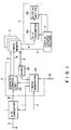
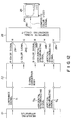
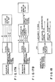
- a digital waveform measuring apparatus will briefly be explained below with reference to Fig. 7.
- a timing signal generating circuit 2c generates a timing signal for each sweep timing dot.
- An address generating circuit 2a receives an input signal and the timing signal and, upon each reception of the timing signal from the timing signal generating circuit, generates an address signal corresponding to each sweep timing dot and to the magnitude of the input signal.
- An image memory 3 stores data in that address.
- a computing section 2b Upon each receipt of the timing signal, a computing section 2b performs a predetermined computation on the data in the image memory 3 and outputs a computation result to the image memory 3.
- a display section 4 displays the input signal with a luminance level corresponding to the computation result.
- an input signal a at an input terminal 8 is supplied to an A/D converter 1 where it is converted to digital waveform data b.
- Digital waveform data b is supplied to a data conversion section 2 comprising an address control section 2a, timing generating section 2c and adder 2b.
- the timing generating section 2c receives a trigger signal c and supplies a predetermined timing signal to the A/D converter 1, address control section 2a and adder 2b.
- the address control section 2a receives the digital waveform data b and generates a row address d corresponding to the digital waveform data level.
- the address control section 2a receives the timing signal i from the timing generating section 2c and generates a column address e corresponding to that timing.
- the generated row address d and column address e (hereinafter referred to merely as an address) are delivered to the image memory 3.
- timing signal i a timing signal which is obtained by dividing sweep time for the measurement into desired time intervals is also used as column address e.
- the adder 2b reads the luminance level data f from the address of the image memory 3, adds a predetermined value L to the data f and writes a result of addition to the same address.
- the predetermined value L is 1 and, upon the result of addition reaching 255, a subsequent addition is stopped.
- the predetermined value L is initially set to the adder 2b.
- a display control section 5 supplies a control signal j to the image memory 3 and the luminance data f is read, as display data h representative of the result of addition, out of the image memory 3 and supplies it to a D/A converter 4a where the display data h is converted to an analog signal.
- the analog signal is supplied to a display section 4b.
- the display section 4b has an image screen of a 512 x 512 dot matrix array. Of these dots of the dot matrix array, that dot corresponding to the address as set forth above is displayed with a luminance level corresponding to the luminance data f which is stored in the address.
- the D/A converter 4a and display section 4b constitute a display unit 4.
- the address control section 2a and adder 2b are constructed of a hardware system made up of a microcomputer including a CPU, ROM and RAM.
- the image memory 3 can store 8-bit-per-dot luminance data.
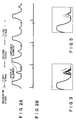
- Fig. 2 shows a waveform of the input signal a and that of the trigger signal c in Fig. 1.
- the input signal is a pulse composed of a stable component and a varying element, that the varying component of the pulse sequentially varies from left to right, as shown, with a time from a first measuring stage to a third measuring stage, that a plurality of pulses are involved ineach measruing stage, and that the trigger signal c is received from outside in synchronism with the pulse as set forth above or generated by comparing a variable threshold level with the aforementioned pulse.
- a start signal g is supplied, for example, from an operation panel, not shown, to the timing generation section 2c.
- the timing generation section 2c supplies an instruction signal to the address control section 2a and adder 2b so that all luminance data f in the image memory 3 may be cleared.
- the measurement is started by the trigger signal c which is input immediately after a start signal g.
- the trigger signal c which is input immediately after a start signal g.
- a time period T from the generation of the trigger signal g becomes one measuring cycle.
- the timing generation section 2c divides the time period T by the number of column address 1 (512 in this case) and generates a timing signal at a divided time interval.
- the timing signal is delivered to the A/D converter 1, address control section 2a, and adder 2b for control purpose.
- the adder 2b adds 1 to the luminance data f corresponding to an address determined by a row address d and column address e and supplies a result of addition to the image memory 3.
- the luminance data f is weighted according to the frequency or existence of the same addresses designated for each sweep timing dot.
- the maximum luminance level of the dot displayed by the luminance data f becomes 256.
- the luminance data f becomes greater and hence the dot appears brighter. If, on the other hand, the trace frequency is decreased, the dot appears darker. More specifically, the level of an input waveform at a particular timing is held by each dot on the display screen for each sweep timing dot. When the frequency of the input waveform of the same level for each sweep timing dot is high, the same dot is swept with a high frequency compared with other dots. therefore, the dot is displayed with a higher luminance level.
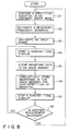
- a repetitive sweeping is performed at step 1 in a normal sweeping mode, that is, in an initializing mode at that turned-on time.
- the measurig frequency band that is, the frequency span and center frequency are set.
- the input range that is, the reference level is set and, at step 4, a shading-tone display is started.
- waveform data which is stored in the image memory 3 is cleared.
- a stop signal is supplied from an operation panel to stop a sweeping operation.
- the shading-tone display is held at step 7.
- it is determined whether or not a measuring operation is again performed. If the answer is in the affirmative, a process following step 4 is implemented. If the answer is in the negative, a process following step 1 is repeated.
- the waveform portion corresponding to the stable component of the pulse is displayed with a brighter luminance level because the configuration of the waveform portion is not varied.
- the waveform portion corresponding to the varying component is distorted in that direction of an arrow in Fig. 3 and displayed with an intermediate tone level. In this embodiment, the waveform remains displayed as it is once it is varied.
- the storage of the data in the image memory 3 may be achieved in any proper way if there is a predetermined relation between the dot position on the image screen determined by an address of the image memory 3 and the luminance level.
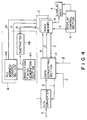
- a digital waveform measuring apparatus according to the second embodiment of the present invention will be explained below by referring to Fig. 4.
- the second embodiment is constructed with an addition of a waveform eliminating circuit 6 to the circuit arrangement shown in Fig. 1.
- the waveform eliminating circuit 6 comprises an all address control section 6a, subtracter 6b and repetition timing generation section 6c.
- the repetition timing generation section 6c supplies a timing signal to the address control section 6a and subtracter 6b.
- the cycle T1 corresponds to the repetition cycle (measuring cycle) T of the timing generation section 2c.
- the all address control section 6a Upon recepit of a timing signal from the repetition timing generation section 6c, the all address control section 6a generates all addresses on the image memory 3, for every cycle T1, which are constructed of combinations of the row addresses n and column address m.
- the subtracter 6b is adapted to subtract a value M from luminance data stored in all the addresses of the image memory 3 for every cycle T1 and to store a result of subtraction back into the image memory 3, noting that the value M denotes a value satisfying a relation L/T > M/T1 .
- the value M is initially set to the subtracter 6b.
- the dot is displayed on the display screen with a maximum luminance level.
- the all address control section 6a and subtraction 6b are constructed of, as in the aforementioned address control section 2a and adder 2b, a microcomputer including a CPU, ROM and RAM. If a synchronizing relation exists between T and T1, the all address control section 6a and subtracter 6b, as well as the address control section 2a and adder 2b, can be constituted by the same microcomputer. Furthermore, the repetition timing generation section 6c can be comprised of the timing generation section 2c.
- the timing relation between the operation of the waveform eliminating circuit 6 and that of the data conversion section 2 is the same as the timing relation between the operation of the waveform eliminating circuit 6 and the display operation of a display unit 4 made by reading the luminance data f, by a display control section 5, out of an image memory 3. That is, the display control section 5 controls the display section 5 so that the display operation is effected for every repetition frequency T2.
- the waveform eliminating circuit 6 is of such a type that, in order to eliminate a signal waveform for every cycle T1, it subtracts M from the luminance data of all addresses of the image memory and stores a result of subtraction back into the address of the image memory 3. In this case, either a synchronous or an asynchronous timing may be taken between the repetition cycle T2 and the cycle T1.
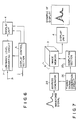
- FIG. 6 A third embodiment of the present invention will be explained below with reference to Fig. 6. This embodiment is similar in arrangement and operation to the previous two embodiments as viewed up to a time at which display data h is input.
- a luminance conversion circuit 7 includes a ROM table and allows an address of the ROM table to be designated upon receipt of display data h so that it is converted to corresponding luminance data.
- the display data h is weighted by luminance data to obtain a linearity and hence to provide an easier-to-observe luminance level.
- the digital waveform measuring apparatus of the present invention performs a digital waveform display by converting the luminance level in accordance with an input signal variation level. It is, thus, possible to observe the signal waveform corresponding to the trace frequency which could not otherwise been implemented in a conversional digital storage oscilloscope. Furthermore, a limitation on the data holding time which is short in the analog storage oscilloscope can substantially been eliminated.
- the luminance data of the image memory can be varied in accordance with the trace frequency, it is possible to readily observe a varying signal waveform. It is also possible to readily and visually observe the signal waveform because the display data is weighted by the luminance conversion circuit.
- Fig. 9A is a view showing the present digital waveform measuring apparatus which is applied to a spectrum analyzer.
- An input signal (a signal to be measured) on an input terminal 18 is mixed with a local oscillation signal (local signal) coming from a local oscillator 11 to obtain an intermediate frequency signal.
- the local oscillation signal of the local oscillator 11 varies in accordance with the level of a sweeping signal from a sweeping signal generator 14.
- the intermediate frequency signal is supplied to a bandpass filter 12 to extract a frequency component corresponding to a passed frequency.
- a signal which is output from the bandpass filter 12 is detected by a detector 13 which in turn generates a DC detection signal corresponding to the output signal level.
- the detection signal is supplied to the aforementioned A/D converter 1 where it is processed in the same way as set forth above in the first embodiment.
- the processed signal is displayed as the detection waveform on a display section 4b.
- a sweep trigger generator 19 is driven by a start signal which is generated by depressing a start switch 50.
- the sweep trigger generator 19 generates a trigger signal repetitively at a given cycle and supplies it to the sweep signal generator 14.
- a sweep signal which is output from the sweep signal generator 14 is supplied to one input terminal of a comparator 15.
- the comparator 15 compares the sweep signal and a signal input to the other input terminal of the comparator 15, and outputs a comparator output signal. When the level of the sweep signal exceeds that of the signal input to the other terminal, the comparator output signal rises, as shown in fig. 9B.
- the rise of the output signal is supplied to the address control section 2a and counter 17.
- the counter 17 is reset by the start signal and adapted to count the rises of received comparator output signals and to deliver a count value to a D/A converter 16.
- the D/A converter 16 converts the count value to an analog signal.
- the analog signal output from the D/A converter 16 reflects the variation (increase) in the count value from the counter 17, and therefore the level of the analog signal is made greater by a given voltage range compared with the signal level generated at the time of the rise in the comparator output signal.
- the analog signal is supplied to the other input terminal.
- the comparator 15 compares the sweep signal which is supplied to one input terminal with a signal which is supplied from the D/A converter 16 to the other input terminal thereof, and detects that the level of the signal from the D/A converter 16 exceeds the sweep signal level, with the result that the comparator output signal falls (Fig. 9B). After this, the above operation is repeated every time the sweep signal level exceeds the output signal level of the D/A converter 16.
- the sweeping operation can be stopped by inputting a stop signal, which is generated by depressing a stop switch 51, to the sweep trigger generator 19 and sweep signal generator 14.
- a digital waveform measuring apparatus according to a fourth embodiment of the present invention will be explained below with respect to Fig. 10.
- the aforementioned digital waveform measuring apparatus includes, as shown in Fig. 19, a display section for displaying a result of measurement. Such a display section is hard to observe in view of being relatively small in dimension. For this reason, it is sometimes necessary to display the waveform characteristic in enlarged format by a monitor TV which is mounted on the outside of the measuring apparatus.
- the measuring apparatus has signal output terminals 21a, 21h and 21v for supplying signals to a monitor TV set.
- the output terminal 21a outputs display data h shown in Fig. 1 as a luminance signal and the output terminals 21h and 21v, respectively, output a horizontal and a vertical synchronizing signal (S h and S v ) from the display control section 5.
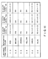
- the digital luminance signal which is supplied as the display data from the image memory 3 in Fig. 1 has, for example, a six-step tone luminance level. If, for example, a voltage level Va of the input signal varies within a range from 0.0 to 1.0, it can be seen that, as shown in Fig. 11,
- the display data h coming from the image memory 3, that is, the digital luminance signal is supplied via the output terminal 21a to data conversion sections 25r, 25g and 25b in a signal conversion device body 22.
- the color signal levels Dr, Dg and Db are ouput to D/A converters 27r, 27g and 27b, respectively, where color signal levels Dr, Dg and Db are converted to R, G and B color signals.
- R, G and B color signals are output to the input terminals 23r, 23g and 23b of a color monitor TV set 23.
- the horizontal synchronizing signal S h and vertical synchronizing signal S v are outut directly to the input terminals 23h and 23v, respectively, without passing through the data conversion sections 25r, 25g and 23v.
- the R, G and B color signals and a color image signal composed of the horizontal synchronizing signal S h and vertical synchronizing S v can be displayed on the color monitor TV23.
- Fig. 19 is a perspective view showing an outer appearance of the digital waveform measuring apparatus.
- the display elements such as the waveform characteristic 102, scale 103, coordinate axes 104, graduation 105, marker 106 and characteristic names 107, are displayed on the display section.
- these display elements are displayed with the mutually different luminance levels.
- the waveform characteristic 102 and marker 106 are displayed with a high luminance level and the scale 103 and so on are displayed with a low luminance level.
- a greater luminance tone level for example, a red color (1.0) is selected for the waveform characteristic 102 and marker 106
- a combination of R, G and B color signals which are output from the D/A converters 27r, 27g and 27b appears red on the image screen as will be seen in Fig. 11.
- the scale is displayed with the low luminance level
- the low luminance tone level for example, a green color (0.2) is selected in the table of Fig. 11 in which case the combination of R, G and B color signals which are output from the D/A converters 27r, 27g and 27b appears green on the display screen.
- the scale 3 is displayed in green color on the display screen of the color TV set 23.
- the measuring data which is displayed in a varying luminance tone level on the monochrome CRT display screen is displayed on the color monitor TV23 in a different color corresponding to the respective luminance tone level. By doing so, a readily reviewable screen is obtained on the color monitor TV set 23.
- Fig. 12 is a block diagram showing a monochrome/color signal conversion apparatus which is employed for a digital waveform measuring apparatus according to a fifth embodiment of the present invention.
- a color monitor TV set 29 is used, having only a composite color signal input terminal 29c for inputting an NTSC type composite color video signal and not having any R, G and B color signals for the color monitor TV set.
- the measuring apparatus 21 delivers a luminance signal and monochrome video signal comprised of a horizontal synchronizing signal h and vertical synchronizing signal v to a signal conversion device body 22 of the same as shown in Fig. 1.
- the luminance signal a is converted to R, G and B color signals at the signal conversion device body 22.
- the R, G and B color signals and horizontal synchronizing signal h and vertical synchronizing v in the color image signal are input to the corresponding signal input terminals 28r, 28g, 28b, 28h and 28v of a composite signal generator 28.
- the composite signal generator 28 is of a conventional type which is employed for transmitting, as an electromagnetic wave, the R, G and B color signals obtained by a color camera at the location of a broadcasting station.
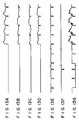
- the respective signal waveforms which are input to the composite signal generator 28 are as shown in Figs. 13A to 13F. That is, the luminance signal waveform is shown in Fig. 13A and the R, G and B color signals and horizontal synchronizing signal h and vertical synchronizing signal v are shown in Figs. 13B, 13C, 13D, 13E and 13F, respectively.
- the composite color video signal having a waveform as shown in Fig. 13G is supplied via an output terminal 28c to a composite color signal input terminal 29c of a color monitor TV set 29.
- the color monitor TV set 29 displays a color image in a color-separation representation corresponding to the luminance tone level of the luminance signal a which is output from the measuring apparatus 21. It is, therefore, possible to obtain substantially the same effect as that of the previous embodiments.
- Fig. 14 is a circuit diagram showing a monochrome/color signal conversion device which is employed in a digital waveform measuring apparatus according to a sixth embodiment of the present invention.
- the same reference numerals are employed in the arrangement shown in Fig. 14 to designate parts or components corresponding to those shown in Fig. 10.
- the luminance signal h′ output from the measuring apparatus 21 corresponds to the output signal from the D/A converter 4a.
- This signal h′ is output from the output terminal 21h as an analog luminance signal, and input to a signal conversion device body 30 shown in Fig. 14.
- the signal conversion device body 30 is composed of three amplifiers 31r, 31g and 31b.
- a luminance signal a which is ouput from the measuring apparatus 21 is supplied to respective amplifiers 31r, 31g and 31b.
- the output signal of the amplifier 31r is input as an R color signal to an R color signal input terminal 23r in a color monitor TV set 23.
- the ouput signal of the amplifier 31g is input as a G color signal to a G color signal input terminal 23g in the color monitor TV set 23.
- the output signal of the amplifier 31b is input as a B color signal to a B color signal input terminal 23b in the color monitor TV set 23.
- the input luminance signal a is input to a positive-side (+) input terminal of a corresponding operational amplifier 33 through an input resistor 32 for determining an amplification factor.
- An offset voltage is applied from a constant voltage source 34 through a variable resistor 35 to the positive-side (+) input terminal of the operational amplifier 33.
- the negative-side (-) input terminal of the amplifier 33 is grounded.
- the luminance signal a is input to a negative-side (-) input terminal of the operational amplifier 33 and a positive-side (+) input terminal of the operational amplifier 33 is grounded.
- the respective amplification factor and respective offset voltage level of the amplifiers 31r, 31g and 31b can be set to any arbitrary values by variably controlling the respective input resistor 32 and respective variable resistor 35. By so setting the respective amplification factor and offset voltage level, it is possible to obtain such an input signal (luminance signal)-to-output signal (respective color signal) characteristic as shown, for example, in Fig. 15.
- the B color signal percentage goes high for a low luminance tone signal of, for example, the scale 3, that is, for the display element of a low luminance tone level and a corresponding area appears substantially green on the display screen of the color monitor TV set 23.
- the R color signal percentage goes high for a high luminance tone signal level of, for example, the waveform characteristic 2, that is, for the display element of a high luminance tone level and a corresponding area appears substantially red on the display screen of the color monitor screen.
- the amplifiers alone are employed in the embodiment of the present invention, making the circuit size compact and hence reducing the manufacturing cost.
- Fig. 16 is a block diagram showing a monochrome/color signal conversion device which is employed in a digital waveform measuring apparatus according to a seventh embodiment of the present invention.
- the same reference numerals are employed in Fig. 16 to designate parts or elements corresponding to those shown in Fig. 14.
- respective R, G and B color signals supplied from three amplifiers 31r, 31g and 31b in a signal conversion device body 30, as well as a horizontal synchronizing signal (H-S) and vertical synchronizing signal (V-S), are supplied to a composite signal genrating circuit 28 of the same type as shown in Fig. 12. These signals are connected by a composite signal generating circuit 28 into a composite color video signal. The composite color video signal is fed to a composite color signal input terminal of a color monitor TV set 29.
- the present invention is not restricted to the aforementioned respective embodiments.
- a signal separation circuit 110 for separating the composite monochrome video signal into the luminance signal and horizontal and vertical synchronizing signals may be incorporated into the signal conversion device body as shown in Fig. 18 to feed respective color signals to the corresponding color signal input terminals of a color monitor TV set or to feed a composite color video signal to a composite color signal input terminal of a color monitor TV set via a composite signal generating circuit as shown in Fig. 17B.
- the fourth to ninth embodiments of the present invention it is possible to display a plurality of display elements, including waveform characteristic, on the screen of the color monitor TV set in a separate color representation by allocating a designated color to respective luminance tone level of the luminance signal in a monochrome video signal which comes from the measuring apparatus. It is thus possible to provide an easier-to-observe display screen at a low cost.
- the luminance signal can be displayed in a different color corresponding to the level of the luminance signal with the use of three amplifiers having a different amplification factor or a different offset voltage. By doing so, an easier-to-observe display screen can be offered at a low cost.
Landscapes
- Physics & Mathematics (AREA)
- General Physics & Mathematics (AREA)
- Testing, Inspecting, Measuring Of Stereoscopic Televisions And Televisions (AREA)
Claims (18)
- Digitale Wellenformmeßvorrichtung, die eine Adreßerzeugungseinrichtung, eine Speichereinrichtung, eine Recheneinrichtung und eine Anzeigeeinrichtung aufweist,
dadurch gekennzeichnet, daß
die Adreßerzeugungseinrichtung (2a) eine Adresse erzeugt, die einem Betrag eines Eingangssignals für jeden Abtasttaktpunkt entspricht;
die Speichereinrichtung (3) Daten speichert, die dem Taktpunkt und der von der Adreßerzeugungseinrichtung (2a) erzeugten Adresse entsprechen;
die Recheneinrichtung (2b) bei Auftreten einer Koinzidenz zwischen einer von der Adreßerzeugungseinrichtung (2b) erzeugten Adresse mit einem gegebenen Abtasttaktpunkt und einer von der Adreßerzeugungseinrichtung (2a) erzeugten Adresse mit dem nächsten Abtasttaktpunkt die Daten, die in der erzeugten Adresse gespeichert sind, mit dem gegebenen Abtasttaktpunkt gewichtet und die gewichteten Daten an den Rahmenpufferspeicher (3) abgibt; und
die Anzeigeeinrichtung (4) die gewichteten Daten von dem Rahmenpufferspeicher (3) empfängt und sie als Wellenform zu Anzeige bringt. - Digitale Wellenformmeßvorrichtung nach Anspruch 1,
dadurch gekennzeichnet, daß
die Gewichtungs-Recheneinrichtung (2b) Farbdaten abgibt, die den Malen des Auftretens der gleichen Adresse, die für jeden Abtasttaktpunkt erzeugt wird, entsprechen. - Digitale Wellenformmeßvorrichtung nach Anspruch 1 oder 2, wobei
eine Taktsignalerzeugungseinrichtung (2c) vorgesehen ist, um ein Taktsignal für jeden Abtasttaktpunkt zu erzeugen; und
die Adreßerzeugungseinrichtung (2a) ein Eingangssignal und das von der Taktsignalerzeugungseinrichtung (2c) erzeugte Taktsignal empfängt und die genannte Adresse entsprechend jedem Abtasttaktpunkt und entsprechend dem Betrag des Eingangssignals bei jedem Empfang des Taktsignals erzeugt, das von der Taktsignalerzeugungseinrichtung (2c) erzeugt wird;
wobei die Gewichtungs-Recheneinrichtung (2b) einen vorbestimmten Rechenvorgang mit den Daten in der Speichereinrichtung (3) jedesmal ausführt, wenn sie das Taktsignal von der Taktsignalerzeugungseinrichtung (2c) empfängt, wobei das Rechenergebnis die Frequenz der gleichen Adresse repräsentiert, die für jeden Abtasttaktpunkt erzeugt wird. - Digitale Wellenformmeßvorrichtung nach Anspruch 3,
dadurch gekennzeichnet, daß
die Adresse eine Zeilenadresse, die dem Betrag des Eingangssignals entspricht, und eine Spaltenadresse, die jedem Abtasttaktpunkt entspricht, aufweist. - Digitale Wellenformmeßvorrichtung nach Anspruch 3,
dadurch gekennzeichnet, daß
die Recheneinrichtung (2b) eine Addiereinrichtung (2b) aufweist, um zu denjenigen Daten, die aus der Adresse der Speichereinrichtung (3) ausgelesen werden, einen vorbestimmten Wert zu addieren und ein Resultat der Addition in diese Adresse einzuschreiben, wobei insbesondere der vorbestimmte Wert variabel ist. - Digitale Wellenformmeßvorrichtung nach Anspruch 5,
dadurch gekennzeichnet, daß
der vorbestimmte Wert 1 ist. - Digitale Wellenformmeßvorrichtung nach Anspruch 3,
dadurch gekennzeichnet, daß
sie ferner eine Subtrahiereinrichtung (6b) aufweist, um von denjenigen Daten, die aus der Adresse der Speichereinrichtung (3) ausgelesen werden, einen vorbestimmten Wert zu subtrahieren und ein Resultat der Subtraktion in diese Adresse einzuschreiben. - Digitale Wellenformmeßvorrichtung nach Anspruch 7,
dadurch gekennzeichnet, daß
sie ferner eine Wiederholungstakterzeugungseinrichtung (6c) aufweist, um einen Takt zu liefern, mit dem eine Subtraktion von der Subtrahiereinrichtung (6b) ausgeführt wird. - Digitale Wellenformmeßvorrichtung nach Anspruch 9,
dadurch gekennzeichnet, daß
sie ferner alle Adreßerzeugungseinrichtungen (6a) aufweist, um ein Taktsignal von der Wiederholungstakterzeugungseinrichtung (6c) zu empfangen und alle Adressen der Speichereinrichtung (3) zu erzeugen. - Digitale Wellenformmeßvorrichtung nach Anspruch 3,
dadurch gekennzeichnet, daß
sie ferner eine Leuchtdichte-Umwandlungseinrichtung (7) aufweist, um ein Ausgangssignal von der Speichereinrichtung (3) zu empfangen und es in vorbestimmte Leuchtdichtedaten umzuwandeln. - Digitale Wellenformmeßvorrichtung nach Anspruch 10,
dadurch gekennzeichnet, daß
die Leuchtdichte-Umwandlungseinrichtung (7) aus einem ROM besteht. - Digitale Wellenformmeßvorrichtung nach Anspruch 3,
dadurch gekennzeichnet, daß
sie ferner aufweist: eine Umwandlungseinrichtung (25r, 25g, 25b), um das Rechenergebnis zu empfangen, das von der Recheneinrichtung (3) abgegeben wird, und um eine entsprechende Vielzahl von Farbsignalen abzugeben, und eine Anzeigeeinrichtung (23), um das Eingangssignal im Farbmodus nach Maßgabe der Vielzahl von Farbsignalen, die von der Umwandlungseinrichtung (25r, 25g, 25b) abgegeben werden, anzuzeigen, wobei insbesondere die Umwandlungseinrichtung (25r, 25g, 25b) auf einem ROM besteht. - Digitale Wellenformmeßvorrichtung nach Anspruch 3,
dadurch gekennzeichnet, daß
sie ferner aufweist: eine Umwandlungseinrichtung (25r, 25g, 25b), um das Recheneregebnis zu empfangen, das von der Recheneinrichtung (3) abgegeben wird, und um eine entsprechende Vielzahl von Farbsignalen abzugeben, eine Einrichtung (28), um die Vielzahl von Farbsignalen, die von der Umwandlungseinrichtung (25r, 25g, 25b) umgewandelt wird, zu empfangen und ein BAS-Signal zu erzeugen, und eine Einrichtung (29), um das BAS-Signal in einem Farbmodus anzuzeigen. - Digitale Wellenformmeßvorrichtung nach Anspruch 12,
dadurch gekennzeichnet, daß
die Umwandlungseinrichtung (25r, 25g, 25b) eine Vielzahl von Verstärkern aufweist, die jeweils einen anderen Verstärkungs(31r, 31g, 31b)-Faktor haben. - Digitale Wellenformmeßvorrichtung nach Anspruch 13,
dadurch gekennzeichnet, daß
die Umwandlungseinrichtung (25r, 25g, 25b) eine Vielzahl von Verstärkern (31r, 31g, 31b) aufweist, die jeweils einen anderen Verstärkungsfaktor haben. - Digitale Wellenformmeßvorrichtung nach Anspruch 3,
dadurch gekennzeichnet, daß
sie ferner aufweist: eine Einrichtung (110), um das Rechenergebnis als ein BAS-Videosignal zu empfangen und um ein Leuchtdichtesignal sowie horizontale und vertikale Synchronisiersignale aus dem BAS-Videosignal abzutrennen, Einrichtungen (25r, 25g, 25b), um das von der Trenneinrichtung (110) abgetrennte Leuchtdichtesignal zu empfangen und eine Vielzahl von Farbsignalen abzugeben, und eine Anzeigeeinrichtung (23), um das Eingangssignal nach Maßgabe der Vielzahl von Farbsignalen, die von der Umwandlungseinrichtung (25r, 25g, 25b) abgegeben werden, anzuzeigen. - Digitale Wellenformmeßvorrichtung nach Anspruch 1,
dadurch gekennzeichnet, daß
sie ferner aufweist: eine Einrichtung (110), um das Rechenergebnis als ein BAS-Videosignal zu empfangen und um es in ein Leuchtdichtesignal und horizontale und vertikale Synchronisiersignale zu trennen, eine Umwandlungseinrichtung (25r, 25g, 25b), um das so abgetrennte Leuchtdichtesignal zu empfangen und eine entsprechende Vielzahl von Farbsignalen abzugeben, eine Einrichtung (28), um die Vielzahl von Farbsignalen, die von der Umwandlungseinrichtung (25r, 25g, 25b) abgegeben werden, zu empfangen und ein BAS-Signal zu erzeugen, und eine Einrichtung (29), um das von der Erzeugungseinrichtung (28) erzeugte BAS-Signal im Farbmodus anzuzeigen. - Digitale Wellenformmeßvorrichtung nach einem der vorhergehenden Ansprüche, die ferner folgendes aufweist:
eine Umwandlungseinrichtung (10) zum Empfangen und zur Frequenzumsetzung eines Eingangssignals;
eine Detektoreinrichtung (13) zur Frequenzdiskriminierung des von der Umwandlungseinrichtung (10) frequenzumgesetzten Eingangssignals und zum Abgeben eines Detektiersignals;
eine Adreßerzeugungseinrichtung (2a) zum Empfangen des von der Taktsignalerzeugungseinrichtung (2c) erzeugten Taktsignals und des von der Detektoreinrichtung (13) detektierten Detektiersignals und zum Erzeugen einer Adresse, die jedem Abtasttaktpunkt und dem Betrag des Detektiersignals entspricht, jeweils bei Empfang des von der Taktsignalerzeugungseinrichtung (2c) erzeugten Taktsignals.
Applications Claiming Priority (4)
| Application Number | Priority Date | Filing Date | Title |
|---|---|---|---|
| JP157629/88 | 1988-06-24 | ||
| JP15762988 | 1988-06-24 | ||
| JP213189 | 1989-01-10 | ||
| JP2131/89 | 1989-01-10 |
Publications (3)
| Publication Number | Publication Date |
|---|---|
| EP0347901A2 EP0347901A2 (de) | 1989-12-27 |
| EP0347901A3 EP0347901A3 (de) | 1991-01-09 |
| EP0347901B1 true EP0347901B1 (de) | 1994-05-04 |
Family
ID=26335454
Family Applications (1)
| Application Number | Title | Priority Date | Filing Date |
|---|---|---|---|
| EP89111366A Expired - Lifetime EP0347901B1 (de) | 1988-06-24 | 1989-06-22 | Messapparat für digitale Wellenformen mit Halbton Abbildung |
Country Status (3)
| Country | Link |
|---|---|
| US (1) | US4940931A (de) |
| EP (1) | EP0347901B1 (de) |
| DE (1) | DE68915063T2 (de) |
Families Citing this family (30)
| Publication number | Priority date | Publication date | Assignee | Title |
|---|---|---|---|---|
| US5032784A (en) * | 1989-04-24 | 1991-07-16 | Smith F Patterson | Spectrum analyzer using sync interconnect |
| US5065147A (en) * | 1989-05-17 | 1991-11-12 | Hewlett-Packard Company | Method and apparatus for simulating analog display in digital display test instrument |
| EP0448322A3 (en) * | 1990-03-23 | 1992-11-25 | Tektronix, Inc. | Automatic extraction of pulseparametrics from multi-valued functions |
| JPH0422874A (ja) * | 1990-05-16 | 1992-01-27 | Matsushita Electric Ind Co Ltd | 波形表示装置 |
| JPH0424611A (ja) * | 1990-05-18 | 1992-01-28 | Seiko Instr Inc | コントラスト自動調整機能付液晶表示装置 |
| US5387896A (en) * | 1990-08-06 | 1995-02-07 | Tektronix, Inc. | Rasterscan display with adaptive decay |
| US5295080A (en) * | 1990-08-06 | 1994-03-15 | Tektronix, Inc. | Method of operating a buffer memory to provide a trigger pattern by storing a trigger code in preselected areas of the buffer memory |
| US5283596A (en) * | 1991-02-05 | 1994-02-01 | Hewlett-Packard Company | Digitally synthesized gray scale for raster scan oscilloscope color display of overlapping multichannel waveforms |
| US5254983A (en) * | 1991-02-05 | 1993-10-19 | Hewlett-Packard Company | Digitally synthesized gray scale for raster scan oscilloscope displays |
| ATE153468T1 (de) * | 1991-04-03 | 1997-06-15 | Magni Systems Inc | Videosimulation einer crt-antwort |
| US5739807A (en) * | 1991-09-13 | 1998-04-14 | Tektronix, Inc. | Method for presenting complex number waveforms |
| USD335093S (en) | 1991-09-23 | 1993-04-27 | Snap-On Tools Corporation | Digital oscilloscope |
| GB2271043B (en) * | 1992-09-21 | 1996-05-22 | Gould Inc | Display resolution enhancement using data compression |
| GB2271699B (en) * | 1992-10-13 | 1997-02-05 | Gould Inc | Display resolution enhancement |
| US5530454A (en) * | 1994-04-13 | 1996-06-25 | Tektronix, Inc. | Digital oscilloscope architecture for signal monitoring with enhanced duty cycle |
| US6151010A (en) * | 1996-05-24 | 2000-11-21 | Lecroy, S.A. | Digital oscilloscope display and method therefor |
| US6269317B1 (en) * | 1997-04-30 | 2001-07-31 | Lecroy Corporation | Self-calibration of an oscilloscope using a square-wave test signal |
| US6246389B1 (en) | 1997-06-03 | 2001-06-12 | Agilent Technologies, Inc. | Simulating analog display slew rate intensity variations in a digital graphics display |
| US6052107A (en) * | 1997-06-18 | 2000-04-18 | Hewlett-Packard Company | Method and apparatus for displaying graticule window data on a computer screen |
| US6104374A (en) * | 1998-02-19 | 2000-08-15 | Tektronix, Inc. | Sparse vector rasterization |
| US6219029B1 (en) | 1998-04-03 | 2001-04-17 | Tektronix, Inc. | Emphasizing infrequent events in a digital oscilloscope having variable intensity rasterizer and variable intensity or color display |
| US6188384B1 (en) * | 1998-06-05 | 2001-02-13 | Tektronix, Inc. | Reacting to unusual waveforms |
| US6163758A (en) * | 1998-06-05 | 2000-12-19 | Tektronix, Inc. | Detection of unusual waveforms |
| US6249115B1 (en) * | 1998-06-25 | 2001-06-19 | Tektronix, Inc. | Method of controlling brightness and contrast in a raster scan digital oscilloscope |
| US6344844B1 (en) * | 1998-08-21 | 2002-02-05 | Agilent Technologies, Inc. | Digital oscilloscope having improved peak detect mode |
| US6239782B1 (en) * | 1999-01-19 | 2001-05-29 | Tektronix, Inc. | Single knob intensity control for use in digital test and measurement equipment |
| US6944559B2 (en) * | 2002-11-22 | 2005-09-13 | Tektronix, Inc. | Channel isolation by switched grounds |
| US20050057253A1 (en) * | 2003-09-03 | 2005-03-17 | Gee Edward C. | Digital phosphor spectrum analyzer |
| CN102053184B (zh) | 2009-11-10 | 2014-06-25 | 北京普源精电科技有限公司 | 一种具有高波形捕获率的数字示波器及其控制方法 |
| CN102565482B (zh) * | 2010-12-31 | 2015-08-19 | 北京普源精电科技有限公司 | 数字示波器及其控制方法 |
Family Cites Families (9)
| Publication number | Priority date | Publication date | Assignee | Title |
|---|---|---|---|---|
| US3787666A (en) * | 1971-10-19 | 1974-01-22 | Nicolet Instrument Corp | Information display system |
| US3838209A (en) * | 1972-06-08 | 1974-09-24 | Matsushita Electric Industrial Co Ltd | Scanning apparatus for a matrix display panel |
| DE2653391C2 (de) * | 1976-11-24 | 1981-12-10 | Standard Elektrik Lorenz Ag, 7000 Stuttgart | Schaltungsanordnung zur Abbildung elektrischer Signale bzw. Funktionen mit Hilfe eines Elektronenstrahl-Oszilloskops |
| JPS5513582A (en) * | 1978-07-13 | 1980-01-30 | Sanyo Electric Co Ltd | Color television receiver |
| US4559535A (en) * | 1982-07-12 | 1985-12-17 | Sigmatron Nova, Inc. | System for displaying information with multiple shades of a color on a thin-film EL matrix display panel |
| JPS62223681A (ja) * | 1986-03-26 | 1987-10-01 | Furuno Electric Co Ltd | レ−ダ装置 |
| JP2515259B2 (ja) * | 1987-07-01 | 1996-07-10 | ダイセル化学工業株式会社 | ピロン−3−カルボキサミド化合物及び除草剤 |
| JPS6417116A (en) * | 1987-07-13 | 1989-01-20 | Seiko Epson Corp | Electronic typewriter |
| GB2214764B (en) * | 1988-01-29 | 1992-01-08 | Tektronix Inc | Pixel intensity modulation in a waveform display |
-
1989
- 1989-06-20 US US07/368,868 patent/US4940931A/en not_active Expired - Fee Related
- 1989-06-22 DE DE68915063T patent/DE68915063T2/de not_active Expired - Fee Related
- 1989-06-22 EP EP89111366A patent/EP0347901B1/de not_active Expired - Lifetime
Also Published As
| Publication number | Publication date |
|---|---|
| DE68915063T2 (de) | 1994-11-03 |
| EP0347901A3 (de) | 1991-01-09 |
| DE68915063D1 (de) | 1994-06-09 |
| US4940931A (en) | 1990-07-10 |
| EP0347901A2 (de) | 1989-12-27 |
Similar Documents
| Publication | Publication Date | Title |
|---|---|---|
| EP0347901B1 (de) | Messapparat für digitale Wellenformen mit Halbton Abbildung | |
| JP3314182B2 (ja) | 試験体のx線レスポンスの視覚画像を表示するための装置および方法 | |
| US4058826A (en) | Method and system for generating oscillographic displays of analog signals upon a TV | |
| US5929842A (en) | Method and apparatus for improving time variant image details on a raster display | |
| US3971068A (en) | Image processing system | |
| US4845553A (en) | Image data compressing device for endoscope | |
| EP1139103A1 (de) | Allzweck-Oszilloskop mit digitaler Fernsehsignalwiedergabefähigkeit | |
| JPS63142981A (ja) | ビデオカメラ装置 | |
| US3792195A (en) | Signal monitor for recurrent electrical signals | |
| EP0398042B1 (de) | Verfahren und Anordnung zur Simulierung einer analogen Anzeige in Test-Instrumenten mit digitaler Anzeige | |
| JP3610273B2 (ja) | デジタル試験測定機器の調整方法及び装置 | |
| JPH0544989B2 (de) | ||
| WO2002039416A1 (fr) | Dispositif de traitement d'image | |
| JP3456639B2 (ja) | ルミナンス成分抽出器及びデジタル蓄積オシロスコープ | |
| US5166779A (en) | Subcarrier to horizontal phase measurement and display for multiple video signals | |
| EP0393824A2 (de) | Lageanzeiger für einen Prüfsignalgenerator | |
| CA1223380A (en) | Displaying waveforms | |
| KR0166624B1 (ko) | 플리커성분 측정장치 | |
| JPH02276972A (ja) | 波形測定装置 | |
| US4504851A (en) | System for monitoring video signal parameters, including the luminance signal | |
| JPH07203476A (ja) | 色画像変換装置 | |
| JP2826966B2 (ja) | ベクトル基準目盛り自動生成装置 | |
| JP2001249149A (ja) | 信号分析装置 | |
| SU843308A1 (ru) | Устройство анализа диаграммы направ-лЕННОСТи иСТОчНиКА СВЕТОВОгО излучЕНи | |
| US3343082A (en) | Raster scanning spectrum analyzer |
Legal Events
| Date | Code | Title | Description |
|---|---|---|---|
| PUAI | Public reference made under article 153(3) epc to a published international application that has entered the european phase |
Free format text: ORIGINAL CODE: 0009012 |
|
| 17P | Request for examination filed |
Effective date: 19890622 |
|
| AK | Designated contracting states |
Kind code of ref document: A2 Designated state(s): DE FR GB |
|
| PUAL | Search report despatched |
Free format text: ORIGINAL CODE: 0009013 |
|
| RHK1 | Main classification (correction) |
Ipc: G01R 13/34 |
|
| AK | Designated contracting states |
Kind code of ref document: A3 Designated state(s): DE FR GB |
|
| 17Q | First examination report despatched |
Effective date: 19920828 |
|
| GRAA | (expected) grant |
Free format text: ORIGINAL CODE: 0009210 |
|
| AK | Designated contracting states |
Kind code of ref document: B1 Designated state(s): DE FR GB |
|
| REF | Corresponds to: |
Ref document number: 68915063 Country of ref document: DE Date of ref document: 19940609 |
|
| ET | Fr: translation filed | ||
| PLBE | No opposition filed within time limit |
Free format text: ORIGINAL CODE: 0009261 |
|
| STAA | Information on the status of an ep patent application or granted ep patent |
Free format text: STATUS: NO OPPOSITION FILED WITHIN TIME LIMIT |
|
| 26N | No opposition filed | ||
| PGFP | Annual fee paid to national office [announced via postgrant information from national office to epo] |
Ref country code: FR Payment date: 19961120 Year of fee payment: 9 |
|
| PG25 | Lapsed in a contracting state [announced via postgrant information from national office to epo] |
Ref country code: FR Free format text: LAPSE BECAUSE OF NON-PAYMENT OF DUE FEES Effective date: 19990226 |
|
| REG | Reference to a national code |
Ref country code: FR Ref legal event code: ST |
|
| PGFP | Annual fee paid to national office [announced via postgrant information from national office to epo] |
Ref country code: GB Payment date: 20010620 Year of fee payment: 13 |
|
| REG | Reference to a national code |
Ref country code: GB Ref legal event code: IF02 |
|
| PG25 | Lapsed in a contracting state [announced via postgrant information from national office to epo] |
Ref country code: GB Free format text: LAPSE BECAUSE OF NON-PAYMENT OF DUE FEES Effective date: 20020622 |
|
| GBPC | Gb: european patent ceased through non-payment of renewal fee |
Effective date: 20020622 |
|
| PGFP | Annual fee paid to national office [announced via postgrant information from national office to epo] |
Ref country code: DE Payment date: 20060615 Year of fee payment: 18 |
|
| PG25 | Lapsed in a contracting state [announced via postgrant information from national office to epo] |
Ref country code: DE Free format text: LAPSE BECAUSE OF NON-PAYMENT OF DUE FEES Effective date: 20080101 |