EP0347560A2 - Memory access control device which can be formed by a reduced number of LSI's - Google Patents
Memory access control device which can be formed by a reduced number of LSI's Download PDFInfo
- Publication number
- EP0347560A2 EP0347560A2 EP89107633A EP89107633A EP0347560A2 EP 0347560 A2 EP0347560 A2 EP 0347560A2 EP 89107633 A EP89107633 A EP 89107633A EP 89107633 A EP89107633 A EP 89107633A EP 0347560 A2 EP0347560 A2 EP 0347560A2
- Authority
- EP
- European Patent Office
- Prior art keywords
- arithmetic
- memory
- circuit
- held
- distance
- Prior art date
- Legal status (The legal status is an assumption and is not a legal conclusion. Google has not performed a legal analysis and makes no representation as to the accuracy of the status listed.)
- Granted
Links
Images


Classifications
-
- G—PHYSICS
- G06—COMPUTING; CALCULATING OR COUNTING
- G06F—ELECTRIC DIGITAL DATA PROCESSING
- G06F12/00—Accessing, addressing or allocating within memory systems or architectures
- G06F12/02—Addressing or allocation; Relocation
- G06F12/06—Addressing a physical block of locations, e.g. base addressing, module addressing, memory dedication
- G06F12/0607—Interleaved addressing
Definitions
- This invention relates to a memory access control device for accessing a memory device to read and/or write a data block consisting of a plurality of data elements from and/or in the memory device.
- the memory access control device is used in a vector processing system or the like.
- a memory access control device of the type described is for use in combination with a memory device which comprises first through p-th memory units and first through p-th ports connected to the first through the p-th memory units, respectively, where p represents an integer greater than one.
- Each of the memory units is assigned with at least one of memory addresses consecutively increasing relative to the first through the p-th memory units in order to read and/or write each of the data elements of the data block from and/or in the memory device.
- the memory access control device is for accessing selected ones of the memory addresses by selecting a base or reference one of the memory addresses and a preselected distance between two adjacent ones of the selected ones of the memory addresses. That is, the base one of the memory addresses is identical with a leading one of the selected addresses.
- a conventional memory access control device comprises an access address producing circuit for simultaneously producing first through p-th access addresses when the preselected distance is a unit distance. That is, the number of the access addresses is equal to the number of the ports. Supposing that the base memory address is represented by B and that the preselected distance is represented by D, the access addresses are represented by (B), (B + D), (B + 2D), ..., and (B + nD), where n represents one of values equal to "0", “1", “2”, ..., and "p - 1".
- a crossbar circuit supplies the first through the p-th access addresses to corresponding ones of the memory units via the first through the p-th ports. As a result, the corresponding ones of the memory units are simultaneously accessed by the first through the p-th access addresses.
- LSI's large scale integration circuits
- a sum of input and output pins which can be formed on an LSI is restricted to a predetermined maximum value as known in the art.
- the number of the input and output pints which are necessary in forming the crossbar circuit by the use of the LSI's increases in direct proportion to a total sum of the number of the ports and the number of the access addresses.
- the access address producing circuit produces the access addresses which are equal in number to the ports as mentioned above, the total sum of the number of the input and the output pins are twice the number of the output pins.
- Each of the access addresses is of, for example, thirty bits.
- a memory access control device to which this invention is applicable is for use in combination with a memory device which comprises a first through a (2 x m)-th memory unit and a first through a (2 x m)-th port connected to the first through the (2 x m)-th memory units, respectively, where m represents an integer greater than one.
- a memory device which comprises a first through a (2 x m)-th memory unit and a first through a (2 x m)-th port connected to the first through the (2 x m)-th memory units, respectively, where m represents an integer greater than one.
- Each of the first through the (2 x m)-th memory units is assigned with at least one of memory addresses consecutively increasing relative to the first through the (2 x m)-th memory units.
- the memory access control device is for accessing selected ones of the memory addresses by selecting a base one of the memory addresses and with a preselected distance left between two adjacent ones of the selected ones of the memory addresses.
- the memory access control device includes base address holding means for holding the base one of the memory addresses as a held base address and distance holding means for holding the preselected distance as a held distance.
- the memory access control device comprises: (1) first through m-th arithmetic means each of which is connected to the base address holding means and the distance holding means to produce an arithmetic result (B + nD) in response to the held base address and the held distance, where B and D are representative of the held base address and the held distance, respectively, while n is representative of one of first through m-th values, the first through the m-th values being equal to "0", "1", ..., and "m - 1", respectively; (2) value distributing means preliminarily given the values and connected to the first through the m-th arithmetic means for distributing the first through the m-th values to the first through the m-th arithmetic means in response to a distributing control signal; (3) distributing control signal producing means connected to the base address holding
- a conventional memory access control device 20 will be described at first for a better understanding of this invention.
- the conventional memory access control device 20 is equivalent to a memory access control device which is described in the preamble of the instant specification.
- the conventional memory access control device 20 is for use in combination with a memory device 21 comprising first through p-th memory units (not shown) each of which is assigned with at least one of memory addresses which consecutively increase in relation to the memory units.
- the memory device 21 further comprises first through p-th ports connected to the first through the p-th memory units, respectively.
- the memory device 21 comprises first through eighth ports 22-1, ..., and 22-8. Therefore, the number of the memory units is equal to eight.
- the memory access control device 20 is for accessing selected ones of the memory addresses at a preselected distance D by selecting a base B of the memory addresses.
- the memory access control device 20 comprises a base address register 23 for holding the base B of the memory addresses as a held base address B and a distance register 24 for holding the preselected distance D as a held distance D.
- the base address register 23 is labelled BR while the distance register 24 is labelled DR.
- the illustrated memory access control device 20 further comprises first through seventh arithmetic circuits 25-1, ..., and 25-7 and first through eighth access address registers 26-1, ..., and 26-8.
- the first access address register 26-1 is connected to the base address register 23 to hold the held base address B as a first access address.
- Each of the first through the fourth arithmetic circuits 25-1, ..., and 25-4 is connected to the base address register 23 and the distance register 24. Responsive to the held base address B and the held distance D, the first through the fourth arithmetic circuits 25-1 to 25-4 produce first through fourth produced addresses (B + D), (B + 2D), (B + 3D), and (B + 4D), respectively. Each of the fifth through the seventh arithmetic circuits 25-5 to 25-7 is connected to the fourth arithmetic circuit 25-4 and the distance register 24.
- the fifth through the seventh arithmetic circuits 25-5 to 25-7 produce fifth through seventh produced addresses (B + 5D), (B + 6D), and (B + 7D), respectively.
- the second through the eighth access address registers 26-2, ..., and 26-8 are connected to the first through the seventh arithmetic circuits 25-1 to 25-7, respectively.
- the first through the seventh produced addresses (B + D), (B + 2D), (B + 3D), (B + 4D), (B + 5D), (B + 6D), and (B + 7D) are held in the second through the eighth access registers 26-2 to 26-8 as second through eighth access addresses, respectively.
- a combination of the first through the seventh arithmetic circuits 25 (suffixes omitted) and the first through the eighth access address registers 26 (suffixes omitted) serves as an access address producing circuit described in the preamble of the instant specification.
- a crossbar circuit 27 is connected to the first through the eighth access address registers 26 and the first through the eighth ports 22 (suffixes omitted) to supply each of the first through the eighth access addresses (B), (B + D), (B + 2D), (B + 3D), (B + 4D), (B + 5D), (B + 6D), and (B + 7D) to one of the first through the eighth ports 22.
- This one of the first through the eighth ports 22 corresponds to one of the memory units that should be accessed by the access address under consideration.
- the number of the LSI's should be increased merely for the purpose of coping with the number of input and output LSI pins as described in the preamble of the instant specification.
- a memory access control device 30 is also for use in combination with the memory device 21.
- the memory device 21 comprises first through q-th memory units and first through q-th ports connected to the first through the q-th memory units, respectively, where q is equal to (2 x m) and where in turn m represents an integer greater than one.
- q and m are equal to eight and four, respectively.
- the illustrated memory device 21 comprises first through eighth memory units 31-1, ..., and 31-8 connected to first through eighth ports 22-1 to 22-8, respectively.
- Each of the memory units 31 (suffixed omitted) is also called a memory module in the art.
- the memory device 21 comprises one hundred and twenty-eight banks. Each of the banks is assigned with one of memory addresses #0, #1, ..., and #127.
- the first memory unit 31-1 consists of sixteen banks of the memory addresses #0, #8, ..., and #120. The banks of the first memory unit 31-1 are connected in common to the first port 22-1.
- the second memory unit 31-2 consists of sixteen banks of the memory addresses #1, #9, ..., and #121.
- the eighth memory unit 31-8 consists of banks of the memory addresses #7, #15, ..., and #127.
- each of the memory units 31 is assigned with at least one of the memory addresses consecutively increasing relative to the first through the eighth memory units 31-1 to 31-8.
- the memory access control device 30 is for accessing selected ones of the memory addresses by selecting a base memory address B among the memory addresses and with a preselected distance D left between two adjacent ones of the selected one of the memory addresses.
- the memory access control device 30 receives a memory access request signal from an external device (not shown)
- the base memory address B and the preselected distance D are held in the base address register 23 and the distance register 24 as the held base address B and the held distance D, respectively.
- An access address producing circuit 32 is connected to the base address register 23 and the distance register 24 through connection lines 33 and 34.
- the access address producing circuit 32 comprises first through m-th arithmetic circuits.
- the access address producing circuit 32 comprises first through fourth arithmetic circuits 35-1, ..., and 35-4, each of which is labelled AC.
- each of the arithmetic circuits 35 (suffixes omitted) is connected to the base address register 23 and the distance register 24. Responsive to the held base address B and the held distance D, each of the arithmetic circuits 35 produces an arithmetic result (B + nD), where n is representative of one of first through m-th values. The first through the m-th values are equal to "0", “1", ..., and "m - 1", respectively. Inasmuch as m is equal to four in the illustrated memory access control device 30, n is representative of one of first through fourth values which are equal to "0", "1", "2", and "3", respectively.
- a crossbar circuit 36 is preliminarily given the first through the fourth values and is connected to the first through the fourth arithmetic circuits 35-1 to 35-4 via first through fourth connection lines 37-1, ..., and 37-4.
- the crossbar circuit 36 distributes the first through the fourth values to the first through the fourth arithmetic circuits 35-1 to 35-4 in response to a distributing control signal (namely, a crossbar control signal) 38. From this viewpoint, the crossbar circuit 36 will be referred to as a value distributing circuit.
- a control section 39 is connected to the base address register 23 and the distance register 24 through connection lines 40 and 41 and also to the crossbar circuit 36. Responsive to the held base address and the held distance, the control section 39 produces the distributing control signal 38. Therefore, the control section 39 will be called a distributing control signal producing circuit.
- the distributing control signal 38 comprises first through third partial control signals 42-1, ..., and 42-3 which will become clear as the description proceeds.
- An arithmetic result distributing circuit 43 is connected to the first through the fourth arithmetic circuits 35-1 to 35-4 and to the first through the eighth ports 22-1 to 22-8.
- the arithmetic result distributing circuit 43 distributes the arithmetic results of the first through the fourth arithmetic circuits 35-1 to 35-4 to the first through the eighth ports 22-1 to 22-8 as the selected ones of the memory addresses.
- the control section 39 comprises an adder 43 connected through the connection lines 40 and 41 to the base address and the distance registers 23 and 24 (Fig. 2).
- a least significant bit namely, a zeroth bit
- a first bit are represented by bx0 and bx1, respectively, when the held base address B is expressed by a binary representation.
- a least significant bit namely, a zeroth bit
- a first bit are represented by dx0 and dx1, respectively, when the held distance D is expressed by a binary representation.
- the first bit is the least significant bit but one.
- the adder 43 receives the combinations BX and DX from the connection lines 40 and 41 and produces an addition result represented by (BX + DX). Still further supposing that a first bit, which is a least significant bit but one of the addition result (BX + DX), is represented by x1, the first bit x1 of the addition result (BX + DX) is delivered to the crossbar circuit 36 as the first partial control signal 42-1.
- the zeroth bit bx0 of the held base address B is delivered to the crossbar circuit 36 as the second partial control signal 42-2.
- the first bit bx1 of the held base address B is delivered to the crossbar circuit 36 as the third partial control signal 42-3.
- the crossbar circuit 36 comprises first through fourth crossbars 44-1, ..., and 44-4.
- the first crossbar 44-1 has first and second input terminals I1 and I2 and first and second output terminals O1 and O2.
- the first and second input terminals I1 and I2 of the first crossbar 44-1 are preliminarily given the first and the third values "0" and "2", respectively.
- the first crossbar 44-1 receives the first partial control signal 42-1 and a first inverted signal, into which the first partial control signal 42-1 is inverted by a first inverter 45.
- the first partial control signal 42-1 is indicative of the first bit x1 of the addition result (BX + DX) of the adder 43 (Fig. 3).
- the first crossbar 44-1 comprises six NAND gates (unnumbered) to distribute the first and the third values "0" and "2" to the first and the second output terminals O1 and O2 thereof in response to the first partial control signal 42-1 and the first inverted signal.
- the second crossbar 44-2 is similar to the first crossbar 44-1 except that first and second input terminals I1 and I2 of the second crossbar 44-2 are preliminarily given the second and the fourth values "1" and "3", respectively, and that the second crossbar 44-2 receives the second partial control signal 42-2 and a second inverted signal, into which the second partial control signal 42-2 is inverted by a second inverter 46.
- the second crossbar 44-2 distributes the second and the fourth values "1" and "3" to first and second output terminals O1 and O2 thereof in response to the second partial control signal 42-2 and the second inverted signal.
- the second partial control signal 42-1 is indicative of the zeroth bit bx0 of the held base address B.
- the third crossbar 44-3 is also similar to the first crossbar 44-1 except that first and second input terminals I1 and I2 of the third crossbar 44-3 are connected to the first output terminals O1 of the first and of the second crossbars 44-1 and 44-2, respectively, and that the third crossbar 44-3 receives the third partial control signal 42-3 and a third inverted signal, into which the third partial control signal 42-3 is inverted by a third inverter 47.
- the third partial control signal 42-3 is indicative of the first bit bx1 of the held base address B.
- the third crossbar 44-3 has first and second output terminals O1 and O2 connected to the first and the second arithmetic circuits 35-1 and 35-2 (Fig. 2) through the first and the second connection lines 37-1 and 37-2, respectively.
- the fourth crossbar 44-4 is similar to the third crossbar 44-3 except that first and second input terminals I1 and I2 of the fourth crossbar 44-4 are connected to the second output terminals O2 of the first and of the second crossbars 44-1 and 44-2, respectively.
- the fourth crossbar 44-4 has first and second output terminals O1 and O2 connected to the third and the fourth arithmetic circuits 35-3 and 35-4 (Fig. 2) through the third and the fourth connection lines 37-3 and 37-4, respectively.
- each of the first through the fourth crossbars 44 (suffixes omitted) when the crossbar 44 under consideration receives the partial control signal 42 (Fig. 4) which has a logic "1" level.
- the crossbar 44 connects the first and the second input terminals I1 and I2 to the second and the first output terminals O2 and O1, respectively, as shown by crossing dashed lines.
- the crossbar 44 connects crosswise the first and the second input terminals I1 and I2 and the first and the second output terminals O1 and O2.
- each of the crossbars 44 when the crossbar 44 under consideration receives the partial control signal 42 which has a logic "0" level.
- the crossbar 44 connects the first and the second input terminals I1 and I2 to the first and the second output terminals O1 and O2, respectively, as shown by parallel dashed lines.
- the first crossbar 44 connects straight the first and the second input terminals I1 and I2 and the first and the second output terminals O1 and O2.
- the crossbar circuit 36 illustrated in Fig. 4 distributes the first through the fourth values "0", “1", “2”, and “3" to the first through the fourth connection lines 37-1 to 37-4 in accordance to the first through the third partial control signals 42-1 to 42-4 in the manner illustrated in Fig. 7.
- the access address producing circuit 32 comprises first through fourth arithmetic circuits 35-1 to 35-4.
- the first arithmetic circuit 35-1 comprises a decoder 49 which is labelled DC and which is connected to the first connection line 37-1.
- An arithmetic unit 50 labelled AU, is connected to the decoder 49 through first and second signal lines 51 and 52 and to the registers 23 and 24 (Fig. 2) through the connection lines 33 and 34 through which the held base address B and the held distance D are supplied, respectively.
- the decoder 49 receives one of the first through the fourth values "0", “1", “2”, and “3” through the first connection line 37-1 and decodes that one of the values into a decoded signal consisting of first and second bit signals.
- the decoder 49 receives the first value "0”
- the first and the second bit signals of the decoded signal have a logic “0” level in common.
- the second value "1” is decoded into the first and the second bit signals which have a logic "1” level and a logic “0” level, respectively.
- the third value "2” is decoded into the first and the second bit signals which have a logic "0” level and a logic “1” level, respectively.
- the fourth value "3" is received, the first and the second bit signals have a logic "1" level in common.
- the first and the second bit signals are supplied to the first and the second signal lines 51 and 52, respectively.
- the first bit signal of a logic "1" level will be referred to as a first enable signal while the second bit signal of a logic "1" level will be called a second enable signal.
- the held base address B is delivered to a first output line 53-1 of the first arithmetic circuit 35-1 as the arithmetic result of the first arithmetic circuit 35-1.
- the arithmetic unit 50 receives only the first enable signal among the first and the second enable signals, the arithmetic unit 50 adds the held base address B and the held distance D together and produces an addition result (B + D) which is supplied to the first output line 53-1 as the arithmetic result.
- the arithmetic unit 50 Upon reception of only the second enable signal among the first and the second enable signals, the arithmetic unit 50 adds the held base address B and twice the held distance D together and produces another addition result (B + 2D) which is supplied to the first output line 53-1 as the arithmetic result.
- the arithmetic unit 50 adds the held base address B, the held distance D, and twice the held distance D together and produces still another addition result (B + 3D) which is supplied to the first output line 53-1 as the arithmetic result.
- each of the second through the fourth arithmetic circuits 35-2 to 35-4 comprises a decoder 49 and an arithmetic unit 50 (the same reference numerals 49 and 50 being used).
- Each of the second through the fourth arithmetic circuits 35-2 to 35-4 is similar to the first arithmetic circuit 35-1 except that the decoders 49 of the second through the fourth arithmetic circuits 35-2 to 35-4 are connected to the second through the fourth connection lines 37-2 to 37-4, respectively, and that the arithmetic results produced by the arithmetic units 50 of the second through the fourth arithmetic circuits 35-2 to 35-4 are supplied to second through the fourth output lines 53-2, ..., and 53-4 of the second through the fourth arithmetic circuits 35-2 to 35-4, respectively.
- First through eighth selectors 54-1, ..., and 54-8 are labelled SE in common.
- a first selector group is composed of the first through the fourth selectors 54-1 to 54-4 while a second selector group is composed of the fifth through the eighth selectors 54-5 to 54-8.
- Each of the first through the fourth selectors 54-1 to 54-4 is connected to the first and the second output lines 53-1 and 53-2 of the first and the second arithmetic circuits 35-1 and 35-2 while each of the fifth through the eighth selectors 54-5 to 54-8 is connected to the third and the fourth output lines 53-3 and 53-4 of the third and the fourth arithmetic circuits 35-3 and 35-4.
- the selector in question selects, as a selected result, one of the arithmetic results received from the first and the second output lines 53-1 and 53-2 of the first and the second arithmetic circuits 35-1 and 35-2.
- the selected result of the selector under consideration is decided by an indication signal 56 indicative of one of the first and the second output lines 53-1 and 53-2 of the first and the second arithmetic circuits 35-1 and 35-2.
- each of the fifth through the sixth selectors 54-5 to 54-8 selects, as another selected result, one of the arithmetic results received from the third and the fourth output lines 53-3 and 53-4 of the third and the fourth arithmetic circuits 35-3 and 35-4 in response to another selector enable signal 57 and another indication signal 58.
- the other indication signal 58 is indicative of one of the third and the fourth output lines 53-3 and 53-4 of the third and the fourth arithmetic circuits 35-3 and 35-4.
- a flip-flop circuit 59 is labelled FF. It will be assumed that each bank of the memory device 21 (Fig. 2) is capable of memorizing a data element of one word.
- a flag of logic "0" level is set in the flip-flop circuit 59 by an instruction controller (not shown) in a first case where the memory access control device 30 (Fig. 2) accesses the memory device 21 in order to read or write each data element of one word from or in each of the banks of the selected ones of the memory addresses. The first case is therefore called a single word access mode in the art.
- Another flag of logic "1" level is set in the flip-flop circuit 59 in a second case where the memory access control device 30 accesses the memory device 21 in order to read or write each data element of two words from or in the memory device 21. The second case is therefore called a double word access mode in the art.
- first and second control circuits 61 and 62 are connected to the flip-flop circuit 59 through a connection line 63. Attention will be directed to the first control circuit 61.
- the first control circuit 61 is also connected to the arithmetic unit 50 of the first arithmetic circuit 35-1 through first and second connection lines 64-1 and 64-2.
- the first control circuit 61 is still further connected to the arithmetic unit 50 of the second arithmetic circuit 35-2 through third and fourth connection lines 64-3 and 64-4.
- a least significant bit (namely, a zeroth bit) and a second bit are represented by A1(0) and A1(2), respectively, and that, in the arithmetic result of the arithmetic unit 50 of the second arithmetic circuit 35-2, a least significant bit (namely, a zeroth bit) and a second bit are represented by A2(0) and A2(2), respectively.
- the second bit A1(2) or A2(2) is the least significant bit but two.
- the first control circuit 61 is supplied with the zeroth and the second bits A1(0) and A1(2) of the arithmetic result of the first arithmetic circuit 35-1 through the first and the second connection lines 64-1 and 64-2.
- the first control circuit 61 is also supplied with the zeroth and the second bits A2(0) and A2(2) of the arithmetic result of the second arithmetic circuit 35-2 through the third and the fourth connection lines 64-3 and 64-4.
- the first control circuit 61 produces a combination of the enable signal 55 and the indication signal 56 and selectively delivers the combination of the enable and the indication signals 55 and 56 to the first through the fourth selectors 54-1 to 54-4 in the manner which will become clear as the description proceeds.
- the second control circuit 62 is connected to the arithmetic unit 50 of the third arithmetic circuit 35-3 through first and second connection lines 66-1 and 66-2.
- the second control circuit 62 is furthermore connected to the arithmetic unit 50 of the fourth arithmetic circuit 35-4 through third and fourth connection lines 66-3 and 66-4.
- a least significant bit (namely, a zeroth bit) and a second bit are represented by A3(0) and A3(2), respectively
- a least significant bit (namely, a zeroth bit) and a second bit are represented by A4(0) and A4(2), respectively.
- the second bit is the least significant bit but two.
- the second control circuit 62 is supplied with the zeroth and the second bits A3(0) and A3(2) of the arithmetic result of the third arithmetic circuit 35-3 through the first and the second connection lines 66-1 and 66-2.
- the second control circuit 62 is also supplied with the zeroth and the second bits A4(0) and A4(2) of the arithmetic result of the fourth arithmetic circuit 35-4 through the third and the fourth connection lines 66-3 and 66-4.
- the second control circuit 62 produces a combination of the enable signal 57 and the indication signal 58 and selectively delivers the combination of the enable and the indication signals 57 and 58 to the fifth through the eighth selectors 54-5 to 54-8 in the manner which will become clear as the description proceeds.
- First through eighth access address registers 67-1, ..., and 67-8 are labelled AR in common and are connected to the first through the eighth selectors 54-1 to 54-8, respectively.
- Each of the access address registers 67 (suffixes omitted) holds the selected result as an access address.
- the first and the second access address registers 67-1 and 67-2 are connected to the first and the second ports 22-1 and 22-2, respectively.
- the third and the fourth access address registers 67-3 and 67-4 are connected to the fifth and the sixth ports 22-5 and 22-6, respectively.
- the fifth, the sixth, the seventh, and the eighth access address registers 67-5, 67-6, 67-7, and 67-8 are connected to the third, the fourth, the seventh, and the eighth ports 22-3, 22-4, 22-7, and 22-8, respectively.
- the access addresses of the access address registers 67 are supplied to the memory device 21 as the selected ones of the memory addresses through the ports 22.
- a combination of the first and the second control circuits 61 and 62, the selectors 54-1 to 54-8, and the access address registers 67-1 to 67-8 serves as the arithmetic result distributing circuit 43 described in conjunction with Fig. 2.
- the first control circuit 61 comprises first through fifth inverters 70-1, ..., and 70-5.
- the first through the fourth inverters 70-1 to 70-4 are connected to the first through the fourth connection lines 64-1 to 64-4, respectively.
- the fifth inverter 70-5 is connected to the connection line 63.
- a first combination of first through sixth NAND gates 71-1, ..., and 71-6 is connected to the first, the second, and the fifth inverters 70-1, 70-2, and 70-5 and to the connection lines 64-1, 64-2, and 63.
- a second combination of first through sixth NAND gates 72-1, ..., and 72-6 is connected to the third, fourth, and the fifth inverters 70-3, 70-4, and 70-5 and to the connection lines 64-3, 64-4, and 63.
- a third combination of first through fourth NAND gates 73-1, ..., and 73-4 is connected to the first combination of the NAND gates 71-1 to 71-6.
- a fourth combination of first through fourth NAND gates 74-1, ..., and 74-4 is connected to the second combination of the NAND gates 72-1 to 72-6.
- the NAND gates 73-1 to 73-4 are connected to the first through the fourth selectors 54-1 to 54-4, respectively, to deliver the selector enable signals 55 to the first through the fourth selectors 54-1 to 54-4, respectively.
- the NAND gates 74-1 to 74-4 are connected to the first through the fourth selectors 54-1 to 54-4, respectively, to deliver the indication signals 56 to the first through the fourth selectors 54-1 to 54-4, respectively.
- the arithmetic result of the first arithmetic circuit 35-1 is selected by one or two enabled selectors of the selectors 54-1 to 54-4 under the control of the first control circuit 61 to deliver the arithmetic result of the first arithmetic circuit 35-1 to the memory device 21.
- the enabled selector is one of the selectors 54-1 to 54-4 that is enabled by the selector enable signal 55 produced by the first control circuit 61.
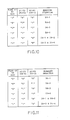
- the first control circuit 61 makes the selectors 54-1 to 54-4 deliver the arithmetic result of the first arithmetic circuit 35-1 to the memory device 21 as shown in Fig. 10.
- "X" represents either "0" or "1".
- the second control circuit 62 is similar to the first control circuit 61 except for the following.
- first through fourth inverters 70-1 to 70-4 are connected to the first through the fourth connection lines 66-1 to 66-4, respectively.
- a first combination of first through sixth NAND gates 71-1 to 71-6 is connected to the connection lines 66-1 and 66-2.
- a second combination of first through sixth NAND gates 72-1 to 72-6 is connected to the connection lines 66-3 and 66-4.
- NAND gates 73-1 to 73-4 are connected to the fifth through the eighth selectors 54-5 to 54-8, respectively, to deliver the selector enable signals 57 to the fifth through the eighth selectors 54-5 to 54-8, respectively.
- NAND gates 74-1 to 74-4 are connected to the fifth through the eighth selectors 54-5 to 54-8, respectively, to deliver the indication signals 58 to the fifth through the eighth selectors 54-5 to 54-8, respectively.
- the arithmetic result of the third arithmetic circuit 35-3 is selected by one or two enabled selectors of the selectors 54-5 to 54-8 under the control of the second control circuit 62 to deliver the arithmetic result of the third arithmetic circuit 35-3 to the memory unit 21.
- the enabled selector is one of the selectors 54-5 to 54-8 that is enabled by the selector enable signal 57 produced by the second control circuit 62.
- the first control circuit 62 makes the selectors 54-5 to 54-8 deliver the arithmetic result of the third arithmetic circuit 35-3 to the memory device 21 as shown in Fig. 13.
- the adder 43 of the control section 39 receives the combinations BX and DX and produces an addition result (BX + DX) which is expressed by a binary representation of "11". Therefore, the first bit x1 of the addition result is equal to "1" and is delivered to the crossbar circuit 36 as the first partial control signal 42-1.
- the control section 39 delivers the zeroth bit bx0, equal to "0", to the crossbar circuit 36 as the second partial control signal 42-2. Simultaneously, the control section 39 delivers the first bit bx1, equal to "1", to the crossbar circuit 36 as the third partial control siganl 42-3.
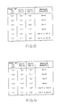
- the crossbar circuit 36 on reception of the first through the third partial control signals 42-1 to 42-3 which have “1", “0”, and “1", respectively, the crossbar circuit 36 operates so that the values "2", "3", "0", and "1" are delivered to the first through the fourth connection lines 37-1 to 37-4, respectively.
- the decoder 49 delivers only the second enable signal to the arithmetic unit 50 through the second signal line 52.
- the arithmetic unit 50 adds the held base address B, equal to "2", and twice the held distance D, equal to "1", together and produces a first addition result "4" which is supplied to the first output line 53-1.
- the zeroth and the second bits A1(0) and A1(2) of the first addition result "4" are equal to "0" and "1", respectively, and are supplied to the first and the second connection lines 64-1 and 64-2, respectively.
- the arithmetic unit 50 receives the first and the second enable signals through the first and the second signal lines 51 and 52. In this event, the arithmetic unit 50 adds the held base address B, equal to "2", the held distance D, equal to "1", and twice the held distance "1" together and produces a second addition result "5" which is supplied to the second output line 53-2.
- the zeroth and the second bits A2(0) and A2(2) of the second addition result "5" are equal to "1" and "1", respectively, and are supplied to the third and the fourth connection lines 64-3 and 64-4, respectively.
- the third arithmetic circuit 35-3 Inasmuch as the third arithmetic circuit 35-3 is supplied with the value "0" through the third connection line 37-3, the third arithmetic circuit 35-3 produces a third addition result "2", equal to the held base address B, to supply the third addition result to the third output line 53-3.
- the zeroth and the second bits A3(0) and A3(2) of the third addition result "2" are equal to "0" and "0", respectively, and are supplied to the first and the second connection lines 66-1 and 66-2, respectively.
- the fourth arithmetic circuit 35-4 adds the held base address B, equal to "2", and the held distance D, equal to "1", together and produces a fourth addition result "3" which is supplied to the fourth output line 53-4.
- the zeroth and the second bits A4(0) and A4(2) of the fourth addition result "3" are equal to "1” and "0", respectively, and are supplied to the third and the fourth connection lines 66-3 and 66-4, respectively.
- the first control circuit 61 controls the selectors 54-1 to 54-4 so that the first addition result "4" of the first output line 53-1 is selected by the third selector 54-3.
- the first addition result "4" is delivered through the fifth port 22-5 to the fifth memory unit 31-5 (Fig. 2) having the bank of the memory address #4.
- the first control circuit 61 also controls the selectors 54-1 to 54-4 so that the second addition result "5" of the second output line 53-2 is selected by the fourth selector 54-4. Therefore, the second addition result "5" is delivered through the sixth port 22-6 to the sixth memory unit 31-6 (Fig. 2) having the bank of the memory address #5.
- the second control circuit 62 controls the selectors 54-5 to 54-8 so that the third addition result "2" of the third output line 53-3 is selected by the fifth selector 54-5.
- the third addition result "2" is delivered through the third port 22-3 to the third memory unit 31-3 (Fig. 2) having the bank of the memory address #2.
- the second control circuit 62 Responsive to the zeroth bit A4(0), equal to "1", and the second bit A4(2), equal to "0", and with reference to the flag "0", the second control circuit 62 also controls the selectors 54-5 to 54-8 so that the fourth addition result "3" of the fourth output line 53-4 is selected by the sixth selector 54-6. As a result, the fourth addition result "3" is delivered through the fourth port 22-4 to the fourth memory unit 31-4 (Fig. 2) having the bank of the memory address #3.
- the memory access control device 30 illustrated in Fig. 2 can access the memory addresses #4, #5, #2, and #3 of the memory device 21 for a particular machine cycle.
- a base memory address "6" is newly held in the base address register 23 by the instruction controller with the unit distance "1" held in the distance register 24.
- the first through the fourth arithmetic circuits 35-1 to 35-4 produce first through fourth arithmetic results "8", "9", "6", and "7", respectively.
- the arithmetic result distributing circuit 43 By the arithmetic result distributing circuit 43, the first through the fourth arithmetic results "8", “9", “6", and “7” are distributed to the first, the second, the seventh, and the eighth memory units 31-1, 31-2, 31-7, and 31-8 which have the banks of the memory addresses #8, #9, #6, and #7, respectively.
Abstract
Description
- This invention relates to a memory access control device for accessing a memory device to read and/or write a data block consisting of a plurality of data elements from and/or in the memory device. The memory access control device is used in a vector processing system or the like.
- A memory access control device of the type described, is for use in combination with a memory device which comprises first through p-th memory units and first through p-th ports connected to the first through the p-th memory units, respectively, where p represents an integer greater than one. Each of the memory units is assigned with at least one of memory addresses consecutively increasing relative to the first through the p-th memory units in order to read and/or write each of the data elements of the data block from and/or in the memory device. The memory access control device is for accessing selected ones of the memory addresses by selecting a base or reference one of the memory addresses and a preselected distance between two adjacent ones of the selected ones of the memory addresses. That is, the base one of the memory addresses is identical with a leading one of the selected addresses.
- As will later be described in conjunction with a figure of accompanying drawing, a conventional memory access control device comprises an access address producing circuit for simultaneously producing first through p-th access addresses when the preselected distance is a unit distance. That is, the number of the access addresses is equal to the number of the ports. Supposing that the base memory address is represented by B and that the preselected distance is represented by D, the access addresses are represented by (B), (B + D), (B + 2D), ..., and (B + nD), where n represents one of values equal to "0", "1", "2", ..., and "p - 1".
- Responsive to the first through the p-th access addresses, a crossbar circuit supplies the first through the p-th access addresses to corresponding ones of the memory units via the first through the p-th ports. As a result, the corresponding ones of the memory units are simultaneously accessed by the first through the p-th access addresses.
- Attention will now be directed to a case where the crossbar circuit is implemented by the use of LSI's (large scale integration circuits). A sum of input and output pins which can be formed on an LSI, is restricted to a predetermined maximum value as known in the art. The number of the input and output pints which are necessary in forming the crossbar circuit by the use of the LSI's, increases in direct proportion to a total sum of the number of the ports and the number of the access addresses. Inasmuch as the access address producing circuit produces the access addresses which are equal in number to the ports as mentioned above, the total sum of the number of the input and the output pins are twice the number of the output pins. Each of the access addresses is of, for example, thirty bits. In this event, the total sum of the number of the input and output pins enormously increases. In order to deal with such a problem related to a great number of pins, it is necessary to increase the number of the LSI's merely for the purpose of coping with the number of the input and the output pins.
- It is therefore an object of this invention to provide a memory access control device which can be formed by a reduced number of LSI's even when a great number of input and output LSI pins are necessary.
- Other objects of this invention will become clear as the description proceeds.
- A memory access control device to which this invention is applicable is for use in combination with a memory device which comprises a first through a (2 x m)-th memory unit and a first through a (2 x m)-th port connected to the first through the (2 x m)-th memory units, respectively, where m represents an integer greater than one. Each of the first through the (2 x m)-th memory units is assigned with at least one of memory addresses consecutively increasing relative to the first through the (2 x m)-th memory units. The memory access control device is for accessing selected ones of the memory addresses by selecting a base one of the memory addresses and with a preselected distance left between two adjacent ones of the selected ones of the memory addresses. The memory access control device includes base address holding means for holding the base one of the memory addresses as a held base address and distance holding means for holding the preselected distance as a held distance. According to this invention, the memory access control device comprises: (1) first through m-th arithmetic means each of which is connected to the base address holding means and the distance holding means to produce an arithmetic result (B + nD) in response to the held base address and the held distance, where B and D are representative of the held base address and the held distance, respectively, while n is representative of one of first through m-th values, the first through the m-th values being equal to "0", "1", ..., and "m - 1", respectively; (2) value distributing means preliminarily given the values and connected to the first through the m-th arithmetic means for distributing the first through the m-th values to the first through the m-th arithmetic means in response to a distributing control signal; (3) distributing control signal producing means connected to the base address holding means, the distance holding means, and the value distributing means for producing the distributing control signal in response to the held base address and the held distance; and (4) arithmetic result distributing means connected to the first through the m-th arithmetic means and the first through the (2 x m)-th ports for distributing the arithmetic results of the first through the m-th arithmetic means to the first through the (2 x m)-th ports as the selected ones of the memory addresses.
-
- Fig. 1 is a block diagram of a conventional memory access control device connected to a memory device;
- Fig. 2 is a block diagram illustrative of a memory access control device according to an embodiment of this invention together with a memory device;
- Fig. 3 is a block diagram of a control section of the memory access control device illustrated in Fig. 2;
- Fig. 4 is a block diagram of a crossbar circuit of the memory access control device illustrated in Fig. 2;
- Fig. 5 is a block diagram for use in describing operation of a crossbar of the crossbar circuit illustrated in Fig. 4;
- Fig. 6 is another block diagram for use in describing another operation of a crossbar of the crossbar circuit illustrated in Fig. 4;
- Fig. 7 is a diagram for use in describing operation of the crossbar circuit illustrated in Fig. 4;
- Fig. 8 is a block diagram of an access address producing circuit of the memory access control device illustrated in Fig. 2;
- Fig. 9 is a block diagram of a first control circuit of the access address producing circuit illustrated in Fig. 8;
- Fig. 10 is a diagram for use in describing operation of the first control circuit illustrated in Fig. 9;
- Fig. 11 is another diagram for use in describing another operation of the first control circuit illustrated in Fig. 9;
- Fig. 12 is a block diagram of a second control circuit of the access address producing circuit illustrated in Fig. 8;
- Fig. 13 is a diagram for use in describing operation of the second control circuit illustrated in Fig. 12; and
- Fig. 14 is another diagram for use in describing another operation of the second control circuit illustrated in Fig. 12.
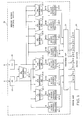
- Referring to Fig. 1, a conventional memory
access control device 20 will be described at first for a better understanding of this invention. The conventional memoryaccess control device 20 is equivalent to a memory access control device which is described in the preamble of the instant specification. - As described in the preamble of the instant specification, the conventional memory
access control device 20 is for use in combination with amemory device 21 comprising first through p-th memory units (not shown) each of which is assigned with at least one of memory addresses which consecutively increase in relation to the memory units. Thememory device 21 further comprises first through p-th ports connected to the first through the p-th memory units, respectively. In the example being illustrated, thememory device 21 comprises first through eighth ports 22-1, ..., and 22-8. Therefore, the number of the memory units is equal to eight. The memoryaccess control device 20 is for accessing selected ones of the memory addresses at a preselected distance D by selecting a base B of the memory addresses. - The memory
access control device 20 comprises abase address register 23 for holding the base B of the memory addresses as a held base address B and adistance register 24 for holding the preselected distance D as a held distance D. Thebase address register 23 is labelled BR while thedistance register 24 is labelled DR. The illustrated memoryaccess control device 20 further comprises first through seventh arithmetic circuits 25-1, ..., and 25-7 and first through eighth access address registers 26-1, ..., and 26-8. The first access address register 26-1 is connected to thebase address register 23 to hold the held base address B as a first access address. - Each of the first through the fourth arithmetic circuits 25-1, ..., and 25-4 is connected to the
base address register 23 and thedistance register 24. Responsive to the held base address B and the held distance D, the first through the fourth arithmetic circuits 25-1 to 25-4 produce first through fourth produced addresses (B + D), (B + 2D), (B + 3D), and (B + 4D), respectively. Each of the fifth through the seventh arithmetic circuits 25-5 to 25-7 is connected to the fourth arithmetic circuit 25-4 and the distance register 24. Responsive to the fourth produced address (B + 4D) and the held distance D, the fifth through the seventh arithmetic circuits 25-5 to 25-7 produce fifth through seventh produced addresses (B + 5D), (B + 6D), and (B + 7D), respectively. - The second through the eighth access address registers 26-2, ..., and 26-8 are connected to the first through the seventh arithmetic circuits 25-1 to 25-7, respectively. The first through the seventh produced addresses (B + D), (B + 2D), (B + 3D), (B + 4D), (B + 5D), (B + 6D), and (B + 7D) are held in the second through the eighth access registers 26-2 to 26-8 as second through eighth access addresses, respectively. Thus, a combination of the first through the seventh arithmetic circuits 25 (suffixes omitted) and the first through the eighth access address registers 26 (suffixes omitted) serves as an access address producing circuit described in the preamble of the instant specification.
- A
crossbar circuit 27 is connected to the first through the eighth access address registers 26 and the first through the eighth ports 22 (suffixes omitted) to supply each of the first through the eighth access addresses (B), (B + D), (B + 2D), (B + 3D), (B + 4D), (B + 5D), (B + 6D), and (B + 7D) to one of the first through the eighth ports 22. This one of the first through the eighth ports 22 corresponds to one of the memory units that should be accessed by the access address under consideration. - When the
crossbar circuit 27 is formed by the use of LSI's, the number of the LSI's should be increased merely for the purpose of coping with the number of input and output LSI pins as described in the preamble of the instant specification. - Referring to Fig. 2, a memory
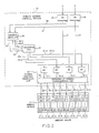
access control device 30 according to a preferred embodiment of this invention is also for use in combination with thememory device 21. Thememory device 21 comprises first through q-th memory units and first through q-th ports connected to the first through the q-th memory units, respectively, where q is equal to (2 x m) and where in turn m represents an integer greater than one. In the illustratedmemory device 21, q and m are equal to eight and four, respectively. More specifically, the illustratedmemory device 21 comprises first through eighth memory units 31-1, ..., and 31-8 connected to first through eighth ports 22-1 to 22-8, respectively. Each of the memory units 31 (suffixed omitted) is also called a memory module in the art. - The
memory device 21 comprises one hundred and twenty-eight banks. Each of the banks is assigned with one of memory addresses #0, #1, ..., and #127. The first memory unit 31-1 consists of sixteen banks of the memory addresses #0, #8, ..., and #120. The banks of the first memory unit 31-1 are connected in common to the first port 22-1. The second memory unit 31-2 consists of sixteen banks of the memory addresses #1, #9, ..., and #121. Likewise, the eighth memory unit 31-8 consists of banks of the memory addresses #7, #15, ..., and #127. Thus, each of the memory units 31 is assigned with at least one of the memory addresses consecutively increasing relative to the first through the eighth memory units 31-1 to 31-8. - Like the memory
access control device 20 illustrated in Fig. 1, the memoryaccess control device 30 is for accessing selected ones of the memory addresses by selecting a base memory address B among the memory addresses and with a preselected distance D left between two adjacent ones of the selected one of the memory addresses. When the memoryaccess control device 30 receives a memory access request signal from an external device (not shown), the base memory address B and the preselected distance D are held in thebase address register 23 and thedistance register 24 as the held base address B and the held distance D, respectively. - An access
address producing circuit 32 is connected to thebase address register 23 and thedistance register 24 throughconnection lines address producing circuit 32 comprises first through m-th arithmetic circuits. In the example being illustrated, the accessaddress producing circuit 32 comprises first through fourth arithmetic circuits 35-1, ..., and 35-4, each of which is labelled AC. - As will later be illustrated, each of the arithmetic circuits 35 (suffixes omitted) is connected to the
base address register 23 and thedistance register 24. Responsive to the held base address B and the held distance D, each of the arithmetic circuits 35 produces an arithmetic result (B + nD), where n is representative of one of first through m-th values. The first through the m-th values are equal to "0", "1", ..., and "m - 1", respectively. Inasmuch as m is equal to four in the illustrated memoryaccess control device 30, n is representative of one of first through fourth values which are equal to "0", "1", "2", and "3", respectively. - A
crossbar circuit 36 is preliminarily given the first through the fourth values and is connected to the first through the fourth arithmetic circuits 35-1 to 35-4 via first through fourth connection lines 37-1, ..., and 37-4. Thecrossbar circuit 36 distributes the first through the fourth values to the first through the fourth arithmetic circuits 35-1 to 35-4 in response to a distributing control signal (namely, a crossbar control signal) 38. From this viewpoint, thecrossbar circuit 36 will be referred to as a value distributing circuit. - A
control section 39 is connected to thebase address register 23 and thedistance register 24 throughconnection lines crossbar circuit 36. Responsive to the held base address and the held distance, thecontrol section 39 produces the distributingcontrol signal 38. Therefore, thecontrol section 39 will be called a distributing control signal producing circuit. The distributingcontrol signal 38 comprises first through third partial control signals 42-1, ..., and 42-3 which will become clear as the description proceeds. - An arithmetic
result distributing circuit 43 is connected to the first through the fourth arithmetic circuits 35-1 to 35-4 and to the first through the eighth ports 22-1 to 22-8. The arithmeticresult distributing circuit 43 distributes the arithmetic results of the first through the fourth arithmetic circuits 35-1 to 35-4 to the first through the eighth ports 22-1 to 22-8 as the selected ones of the memory addresses. - Referring to Fig. 3, the
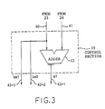
control section 39 comprises anadder 43 connected through the connection lines 40 and 41 to the base address and the distance registers 23 and 24 (Fig. 2). It will be assumed that, in the held base address B, a least significant bit (namely, a zeroth bit) and a first bit are represented by bx0 and bx1, respectively, when the held base address B is expressed by a binary representation. It will also be assumed that, in the held distance D, a least significant bit (namely, a zeroth bit) and a first bit are represented by dx0 and dx1, respectively, when the held distance D is expressed by a binary representation. The first bit is the least significant bit but one. - Further supposing that a combination of the zeroth and the first bits bx0 and bx1 of the held base address B is represented by BX and that another combination of the zeroth and the first bits dx0 and dx1 of the held distance D is represented by DX, the
adder 43 receives the combinations BX and DX from the connection lines 40 and 41 and produces an addition result represented by (BX + DX). Still further supposing that a first bit, which is a least significant bit but one of the addition result (BX + DX), is represented by x1, the first bit x1 of the addition result (BX + DX) is delivered to thecrossbar circuit 36 as the first partial control signal 42-1. - The zeroth bit bx0 of the held base address B is delivered to the
crossbar circuit 36 as the second partial control signal 42-2. The first bit bx1 of the held base address B is delivered to thecrossbar circuit 36 as the third partial control signal 42-3. - Turning to Fig. 4, the
crossbar circuit 36 comprises first through fourth crossbars 44-1, ..., and 44-4. The first crossbar 44-1 has first and second input terminals I1 and I2 and first and second output terminals O1 and O2. The first and second input terminals I1 and I2 of the first crossbar 44-1 are preliminarily given the first and the third values "0" and "2", respectively. The first crossbar 44-1 receives the first partial control signal 42-1 and a first inverted signal, into which the first partial control signal 42-1 is inverted by afirst inverter 45. As mentioned above, the first partial control signal 42-1 is indicative of the first bit x1 of the addition result (BX + DX) of the adder 43 (Fig. 3). The first crossbar 44-1 comprises six NAND gates (unnumbered) to distribute the first and the third values "0" and "2" to the first and the second output terminals O1 and O2 thereof in response to the first partial control signal 42-1 and the first inverted signal. - The second crossbar 44-2 is similar to the first crossbar 44-1 except that first and second input terminals I1 and I2 of the second crossbar 44-2 are preliminarily given the second and the fourth values "1" and "3", respectively, and that the second crossbar 44-2 receives the second partial control signal 42-2 and a second inverted signal, into which the second partial control signal 42-2 is inverted by a
second inverter 46. The second crossbar 44-2 distributes the second and the fourth values "1" and "3" to first and second output terminals O1 and O2 thereof in response to the second partial control signal 42-2 and the second inverted signal. The second partial control signal 42-1 is indicative of the zeroth bit bx0 of the held base address B. - The third crossbar 44-3 is also similar to the first crossbar 44-1 except that first and second input terminals I1 and I2 of the third crossbar 44-3 are connected to the first output terminals O1 of the first and of the second crossbars 44-1 and 44-2, respectively, and that the third crossbar 44-3 receives the third partial control signal 42-3 and a third inverted signal, into which the third partial control signal 42-3 is inverted by a
third inverter 47. The third partial control signal 42-3 is indicative of the first bit bx1 of the held base address B. The third crossbar 44-3 has first and second output terminals O1 and O2 connected to the first and the second arithmetic circuits 35-1 and 35-2 (Fig. 2) through the first and the second connection lines 37-1 and 37-2, respectively. - The fourth crossbar 44-4 is similar to the third crossbar 44-3 except that first and second input terminals I1 and I2 of the fourth crossbar 44-4 are connected to the second output terminals O2 of the first and of the second crossbars 44-1 and 44-2, respectively. The fourth crossbar 44-4 has first and second output terminals O1 and O2 connected to the third and the fourth arithmetic circuits 35-3 and 35-4 (Fig. 2) through the third and the fourth connection lines 37-3 and 37-4, respectively.
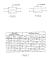
- Turning to Fig. 5, description will proceed to operation of each of the first through the fourth crossbars 44 (suffixes omitted) when the
crossbar 44 under consideration receives the partial control signal 42 (Fig. 4) which has a logic "1" level. In this event, thecrossbar 44 connects the first and the second input terminals I1 and I2 to the second and the first output terminals O2 and O1, respectively, as shown by crossing dashed lines. In other words, thecrossbar 44 connects crosswise the first and the second input terminals I1 and I2 and the first and the second output terminals O1 and O2. - Turning to Fig. 6, description will proceed to operation of each of the
crossbars 44 when thecrossbar 44 under consideration receives the partial control signal 42 which has a logic "0" level. In this event, thecrossbar 44 connects the first and the second input terminals I1 and I2 to the first and the second output terminals O1 and O2, respectively, as shown by parallel dashed lines. In other words, thefirst crossbar 44 connects straight the first and the second input terminals I1 and I2 and the first and the second output terminals O1 and O2. - As a result, the
crossbar circuit 36 illustrated in Fig. 4 distributes the first through the fourth values "0", "1", "2", and "3" to the first through the fourth connection lines 37-1 to 37-4 in accordance to the first through the third partial control signals 42-1 to 42-4 in the manner illustrated in Fig. 7. - Referring to Fig. 8, description will proceed to the access
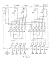
address producing circuit 32. As described above in conjunction with Fig. 2, the accessaddress producing circuit 32 comprises first through fourth arithmetic circuits 35-1 to 35-4. - Attention will be directed to the first arithmetic circuit 35-1. The first arithmetic circuit 35-1 comprises a
decoder 49 which is labelled DC and which is connected to the first connection line 37-1. Anarithmetic unit 50, labelled AU, is connected to thedecoder 49 through first andsecond signal lines registers 23 and 24 (Fig. 2) through the connection lines 33 and 34 through which the held base address B and the held distance D are supplied, respectively. - The
decoder 49 receives one of the first through the fourth values "0", "1", "2", and "3" through the first connection line 37-1 and decodes that one of the values into a decoded signal consisting of first and second bit signals. When thedecoder 49 receives the first value "0", the first and the second bit signals of the decoded signal have a logic "0" level in common. The second value "1" is decoded into the first and the second bit signals which have a logic "1" level and a logic "0" level, respectively. Likewise, the third value "2" is decoded into the first and the second bit signals which have a logic "0" level and a logic "1" level, respectively. When the fourth value "3" is received, the first and the second bit signals have a logic "1" level in common. - The first and the second bit signals are supplied to the first and the
second signal lines - When the
arithmetic unit 50 receives neither the first enable signal nor the second enable signal, the held base address B is delivered to a first output line 53-1 of the first arithmetic circuit 35-1 as the arithmetic result of the first arithmetic circuit 35-1. When thearithmetic unit 50 receives only the first enable signal among the first and the second enable signals, thearithmetic unit 50 adds the held base address B and the held distance D together and produces an addition result (B + D) which is supplied to the first output line 53-1 as the arithmetic result. Upon reception of only the second enable signal among the first and the second enable signals, thearithmetic unit 50 adds the held base address B and twice the held distance D together and produces another addition result (B + 2D) which is supplied to the first output line 53-1 as the arithmetic result. When the first and the second enable signals are received, thearithmetic unit 50 adds the held base address B, the held distance D, and twice the held distance D together and produces still another addition result (B + 3D) which is supplied to the first output line 53-1 as the arithmetic result. - Like the first arithmetic circuit 35-1, each of the second through the fourth arithmetic circuits 35-2 to 35-4 comprises a
decoder 49 and an arithmetic unit 50 (thesame reference numerals decoders 49 of the second through the fourth arithmetic circuits 35-2 to 35-4 are connected to the second through the fourth connection lines 37-2 to 37-4, respectively, and that the arithmetic results produced by thearithmetic units 50 of the second through the fourth arithmetic circuits 35-2 to 35-4 are supplied to second through the fourth output lines 53-2, ..., and 53-4 of the second through the fourth arithmetic circuits 35-2 to 35-4, respectively. - First through eighth selectors 54-1, ..., and 54-8 are labelled SE in common. A first selector group is composed of the first through the fourth selectors 54-1 to 54-4 while a second selector group is composed of the fifth through the eighth selectors 54-5 to 54-8. Each of the first through the fourth selectors 54-1 to 54-4 is connected to the first and the second output lines 53-1 and 53-2 of the first and the second arithmetic circuits 35-1 and 35-2 while each of the fifth through the eighth selectors 54-5 to 54-8 is connected to the third and the fourth output lines 53-3 and 53-4 of the third and the fourth arithmetic circuits 35-3 and 35-4.
- When each of the first through the fourth selectors 54-1 to 54-4 is supplied with a selector enable
signal 55, the selector in question selects, as a selected result, one of the arithmetic results received from the first and the second output lines 53-1 and 53-2 of the first and the second arithmetic circuits 35-1 and 35-2. The selected result of the selector under consideration is decided by anindication signal 56 indicative of one of the first and the second output lines 53-1 and 53-2 of the first and the second arithmetic circuits 35-1 and 35-2. - Likewise, each of the fifth through the sixth selectors 54-5 to 54-8 selects, as another selected result, one of the arithmetic results received from the third and the fourth output lines 53-3 and 53-4 of the third and the fourth arithmetic circuits 35-3 and 35-4 in response to another selector enable
signal 57 and anotherindication signal 58. Theother indication signal 58 is indicative of one of the third and the fourth output lines 53-3 and 53-4 of the third and the fourth arithmetic circuits 35-3 and 35-4. - A flip-
flop circuit 59 is labelled FF. It will be assumed that each bank of the memory device 21 (Fig. 2) is capable of memorizing a data element of one word. A flag of logic "0" level is set in the flip-flop circuit 59 by an instruction controller (not shown) in a first case where the memory access control device 30 (Fig. 2) accesses thememory device 21 in order to read or write each data element of one word from or in each of the banks of the selected ones of the memory addresses. The first case is therefore called a single word access mode in the art. Another flag of logic "1" level is set in the flip-flop circuit 59 in a second case where the memoryaccess control device 30 accesses thememory device 21 in order to read or write each data element of two words from or in thememory device 21. The second case is therefore called a double word access mode in the art. - Each of first and
second control circuits flop circuit 59 through aconnection line 63. Attention will be directed to thefirst control circuit 61. Thefirst control circuit 61 is also connected to thearithmetic unit 50 of the first arithmetic circuit 35-1 through first and second connection lines 64-1 and 64-2. Thefirst control circuit 61 is still further connected to thearithmetic unit 50 of the second arithmetic circuit 35-2 through third and fourth connection lines 64-3 and 64-4. - It will be assumed that, in the arithmetic result of the
arithmetic unit 50 of the first arithmetic circuit 35-1, a least significant bit (namely, a zeroth bit) and a second bit are represented by A1(0) and A1(2), respectively, and that, in the arithmetic result of thearithmetic unit 50 of the second arithmetic circuit 35-2, a least significant bit (namely, a zeroth bit) and a second bit are represented by A2(0) and A2(2), respectively. It should be noted that the second bit A1(2) or A2(2) is the least significant bit but two. - The
first control circuit 61 is supplied with the zeroth and the second bits A1(0) and A1(2) of the arithmetic result of the first arithmetic circuit 35-1 through the first and the second connection lines 64-1 and 64-2. Thefirst control circuit 61 is also supplied with the zeroth and the second bits A2(0) and A2(2) of the arithmetic result of the second arithmetic circuit 35-2 through the third and the fourth connection lines 64-3 and 64-4. In accordance with the zeroth and the second bits A1(0) and A1(2) and the zeroth and the second bits A2(0) and A2(2) and with reference to the flag set into the flip-flop circuit 59, thefirst control circuit 61 produces a combination of theenable signal 55 and theindication signal 56 and selectively delivers the combination of the enable and the indication signals 55 and 56 to the first through the fourth selectors 54-1 to 54-4 in the manner which will become clear as the description proceeds. - Attention will be directed to the
second control circuit 62. Thesecond control circuit 62 is connected to thearithmetic unit 50 of the third arithmetic circuit 35-3 through first and second connection lines 66-1 and 66-2. Thesecond control circuit 62 is furthermore connected to thearithmetic unit 50 of the fourth arithmetic circuit 35-4 through third and fourth connection lines 66-3 and 66-4. - It will be assumed that, in the arithmetic result of the
arithmetic unit 50 of the third arithmetic circuit 35-3, a least significant bit (namely, a zeroth bit) and a second bit are represented by A3(0) and A3(2), respectively, and that, in the arithmetic result of thearithmetic unit 50 of the fourth arithmetic circuit 35-4, a least significant bit (namely, a zeroth bit) and a second bit are represented by A4(0) and A4(2), respectively. The second bit is the least significant bit but two. - The
second control circuit 62 is supplied with the zeroth and the second bits A3(0) and A3(2) of the arithmetic result of the third arithmetic circuit 35-3 through the first and the second connection lines 66-1 and 66-2. Thesecond control circuit 62 is also supplied with the zeroth and the second bits A4(0) and A4(2) of the arithmetic result of the fourth arithmetic circuit 35-4 through the third and the fourth connection lines 66-3 and 66-4. In accordance with the zeroth and the second bits A3(0) and A3(2) and the zeroth and the second bits A4(0) and A4(2) and with reference to the flag set in the flip-flop circuit 59, thesecond control circuit 62 produces a combination of theenable signal 57 and theindication signal 58 and selectively delivers the combination of the enable and the indication signals 57 and 58 to the fifth through the eighth selectors 54-5 to 54-8 in the manner which will become clear as the description proceeds. - First through eighth access address registers 67-1, ..., and 67-8 are labelled AR in common and are connected to the first through the eighth selectors 54-1 to 54-8, respectively. Each of the access address registers 67 (suffixes omitted) holds the selected result as an access address.
- The first and the second access address registers 67-1 and 67-2 are connected to the first and the second ports 22-1 and 22-2, respectively. The third and the fourth access address registers 67-3 and 67-4 are connected to the fifth and the sixth ports 22-5 and 22-6, respectively. The fifth, the sixth, the seventh, and the eighth access address registers 67-5, 67-6, 67-7, and 67-8 are connected to the third, the fourth, the seventh, and the eighth ports 22-3, 22-4, 22-7, and 22-8, respectively.
- The access addresses of the access address registers 67 are supplied to the
memory device 21 as the selected ones of the memory addresses through the ports 22. A combination of the first and thesecond control circuits result distributing circuit 43 described in conjunction with Fig. 2. - Turning to Fig. 9, the
first control circuit 61 comprises first through fifth inverters 70-1, ..., and 70-5. The first through the fourth inverters 70-1 to 70-4 are connected to the first through the fourth connection lines 64-1 to 64-4, respectively. The fifth inverter 70-5 is connected to theconnection line 63. - In the manner illustrated, a first combination of first through sixth NAND gates 71-1, ..., and 71-6 is connected to the first, the second, and the fifth inverters 70-1, 70-2, and 70-5 and to the connection lines 64-1, 64-2, and 63. A second combination of first through sixth NAND gates 72-1, ..., and 72-6 is connected to the third, fourth, and the fifth inverters 70-3, 70-4, and 70-5 and to the connection lines 64-3, 64-4, and 63. A third combination of first through fourth NAND gates 73-1, ..., and 73-4 is connected to the first combination of the NAND gates 71-1 to 71-6. A fourth combination of first through fourth NAND gates 74-1, ..., and 74-4 is connected to the second combination of the NAND gates 72-1 to 72-6.
- The NAND gates 73-1 to 73-4 are connected to the first through the fourth selectors 54-1 to 54-4, respectively, to deliver the selector enable signals 55 to the first through the fourth selectors 54-1 to 54-4, respectively. The NAND gates 74-1 to 74-4 are connected to the first through the fourth selectors 54-1 to 54-4, respectively, to deliver the indication signals 56 to the first through the fourth selectors 54-1 to 54-4, respectively.
- Turning back to Fig. 8, the arithmetic result of the first arithmetic circuit 35-1 is selected by one or two enabled selectors of the selectors 54-1 to 54-4 under the control of the
first control circuit 61 to deliver the arithmetic result of the first arithmetic circuit 35-1 to thememory device 21. The enabled selector is one of the selectors 54-1 to 54-4 that is enabled by the selector enablesignal 55 produced by thefirst control circuit 61. Conditioned by the flag set in the flip-flop circuit 59 and the zeroth and the second bits A1(0) and A1(2) of the arithmetic result of the first arithmetic circuit 35-1, thefirst control circuit 61 makes the selectors 54-1 to 54-4 deliver the arithmetic result of the first arithmetic circuit 35-1 to thememory device 21 as shown in Fig. 10. In Fig. 10, "X" represents either "0" or "1". - For the arithmetic result of the second arithmetic circuit 35-2, conditions are shown in Fig. 11 under which the arithmetic result of the second arithmetic circuit 35-2 is delivered to the
memory device 21. - Turning to Fig. 12, the
second control circuit 62 is similar to thefirst control circuit 61 except for the following. In thesecond control circuit 62, first through fourth inverters 70-1 to 70-4 are connected to the first through the fourth connection lines 66-1 to 66-4, respectively. A first combination of first through sixth NAND gates 71-1 to 71-6 is connected to the connection lines 66-1 and 66-2. A second combination of first through sixth NAND gates 72-1 to 72-6 is connected to the connection lines 66-3 and 66-4. - NAND gates 73-1 to 73-4 are connected to the fifth through the eighth selectors 54-5 to 54-8, respectively, to deliver the selector enable signals 57 to the fifth through the eighth selectors 54-5 to 54-8, respectively. NAND gates 74-1 to 74-4 are connected to the fifth through the eighth selectors 54-5 to 54-8, respectively, to deliver the indication signals 58 to the fifth through the eighth selectors 54-5 to 54-8, respectively.
- Turning back to Fig. 8, the arithmetic result of the third arithmetic circuit 35-3 is selected by one or two enabled selectors of the selectors 54-5 to 54-8 under the control of the
second control circuit 62 to deliver the arithmetic result of the third arithmetic circuit 35-3 to thememory unit 21. The enabled selector is one of the selectors 54-5 to 54-8 that is enabled by the selector enablesignal 57 produced by thesecond control circuit 62. Conditioned by the flag set in the flip-flop circuit 59 and the zeroth and the second bits A3(0) and A3(2) of the arithmetic result of the third arithmetic circuit 35-3, thefirst control circuit 62 makes the selectors 54-5 to 54-8 deliver the arithmetic result of the third arithmetic circuit 35-3 to thememory device 21 as shown in Fig. 13. - For the arithmetic result of the fourth arithmetic circuit 35-4, conditions are shown in Fig. 14 under which the arithmetic result of the fourth arithmetic circuit 35-4 is delivered to the
memory device 21. - Referring to Fig. 2, description will proceed to operation of the memory
access control device 30 when the base memory address "2" and the preselected distance "1" (namely, a unit distance) are held in thebase address register 23 and thedistance register 24 as the held base address and the held distance, respectively. The held base address is expressed by a binary representation of "10" while the held distance is expressed by a binary representation of "01". Therefore, the first and the zeroth bits bx1 and bx0 of the held base address are equal to "1" and "0", respectively. The first and the zeroth bits dx1 and dx0 of the held distance are equal to "0" and "1", respectively. A combination BX of the first and the zeroth bits bx1 and bx0 and another combination DX of the first and the zeroth bits dx1 and dx0 are supplied to thecontrol section 39. - Referring to Figs. 2 and 3, the
adder 43 of thecontrol section 39 receives the combinations BX and DX and produces an addition result (BX + DX) which is expressed by a binary representation of "11". Therefore, the first bit x1 of the addition result is equal to "1" and is delivered to thecrossbar circuit 36 as the first partial control signal 42-1. Thecontrol section 39 delivers the zeroth bit bx0, equal to "0", to thecrossbar circuit 36 as the second partial control signal 42-2. Simultaneously, thecontrol section 39 delivers the first bit bx1, equal to "1", to thecrossbar circuit 36 as the third partial control siganl 42-3. - Referring to Figs. 4 and 7, on reception of the first through the third partial control signals 42-1 to 42-3 which have "1", "0", and "1", respectively, the
crossbar circuit 36 operates so that the values "2", "3", "0", and "1" are delivered to the first through the fourth connection lines 37-1 to 37-4, respectively. - Referring to Figs. 2 and 8, description will proceed to the access
address producing circuit 32. Attention will be directed to the first arithmetic circuit 35-1. Inasmuch as thedecoder 49 is supplied with the value "2" through the first connection line 37-1, thedecoder 49 delivers only the second enable signal to thearithmetic unit 50 through thesecond signal line 52. Upon reception of only the second enable signal among the first and the second enable signals, thearithmetic unit 50 adds the held base address B, equal to "2", and twice the held distance D, equal to "1", together and produces a first addition result "4" which is supplied to the first output line 53-1. The zeroth and the second bits A1(0) and A1(2) of the first addition result "4" are equal to "0" and "1", respectively, and are supplied to the first and the second connection lines 64-1 and 64-2, respectively. - Attention will be directed to the second arithmetic circuit 35-2. Inasmuch as the
decoder 49 is supplied with the value "3" through the second connection line 37-2, thearithmetic unit 50 receives the first and the second enable signals through the first and thesecond signal lines arithmetic unit 50 adds the held base address B, equal to "2", the held distance D, equal to "1", and twice the held distance "1" together and produces a second addition result "5" which is supplied to the second output line 53-2. The zeroth and the second bits A2(0) and A2(2) of the second addition result "5" are equal to "1" and "1", respectively, and are supplied to the third and the fourth connection lines 64-3 and 64-4, respectively. - Inasmuch as the third arithmetic circuit 35-3 is supplied with the value "0" through the third connection line 37-3, the third arithmetic circuit 35-3 produces a third addition result "2", equal to the held base address B, to supply the third addition result to the third output line 53-3. The zeroth and the second bits A3(0) and A3(2) of the third addition result "2" are equal to "0" and "0", respectively, and are supplied to the first and the second connection lines 66-1 and 66-2, respectively.
- Supplied with the value "1" through the fourth connection line 37-4, the fourth arithmetic circuit 35-4 adds the held base address B, equal to "2", and the held distance D, equal to "1", together and produces a fourth addition result "3" which is supplied to the fourth output line 53-4. The zeroth and the second bits A4(0) and A4(2) of the fourth addition result "3" are equal to "1" and "0", respectively, and are supplied to the third and the fourth connection lines 66-3 and 66-4, respectively.
- Referring to Figs. 8, 9, 10 and 11, description will proceed to the
first control circuit 61. It will be assumed that a flag of logic "0" level is set in the flip-flop circuit 59. That is, the memory access control device 30 (Fig. 2) is put into the single word access mode described before. Responsive to the zeroth bit A1(0), equal to "0", and the second bit A1(2), equal to "1", and with reference to the flag "0", thefirst control circuit 61 controls the selectors 54-1 to 54-4 so that the first addition result "4" of the first output line 53-1 is selected by the third selector 54-3. As a result, the first addition result "4" is delivered through the fifth port 22-5 to the fifth memory unit 31-5 (Fig. 2) having the bank of thememory address # 4. - Responsive to the zeroth bit A2(0), equal to "1", and the second bit A2(2), equal to "1", and with reference to the flag "0", the
first control circuit 61 also controls the selectors 54-1 to 54-4 so that the second addition result "5" of the second output line 53-2 is selected by the fourth selector 54-4. Therefore, the second addition result "5" is delivered through the sixth port 22-6 to the sixth memory unit 31-6 (Fig. 2) having the bank of thememory address # 5. - Referring to Figs. 8, 12, 13 and 14, description will proceed to the
second control circuit 62. Responsive to the zeroth bit A3(0), equal to "0", and the second bit A3(2), equal to "0", and with reference to the flag "0", thesecond control circuit 62 controls the selectors 54-5 to 54-8 so that the third addition result "2" of the third output line 53-3 is selected by the fifth selector 54-5. As a result, the third addition result "2" is delivered through the third port 22-3 to the third memory unit 31-3 (Fig. 2) having the bank of thememory address # 2. - Responsive to the zeroth bit A4(0), equal to "1", and the second bit A4(2), equal to "0", and with reference to the flag "0", the
second control circuit 62 also controls the selectors 54-5 to 54-8 so that the fourth addition result "3" of the fourth output line 53-4 is selected by the sixth selector 54-6. As a result, the fourth addition result "3" is delivered through the fourth port 22-4 to the fourth memory unit 31-4 (Fig. 2) having the bank of thememory address # 3. - Thus, the memory
access control device 30 illustrated in Fig. 2 can access the memory addresses #4, #5, #2, and #3 of thememory device 21 for a particular machine cycle. For a next machine cycle which follows the particular machine cycle, a base memory address "6" is newly held in the base address register 23 by the instruction controller with the unit distance "1" held in thedistance register 24. In this case, the first through the fourth arithmetic circuits 35-1 to 35-4 produce first through fourth arithmetic results "8", "9", "6", and "7", respectively. By the arithmeticresult distributing circuit 43, the first through the fourth arithmetic results "8", "9", "6", and "7" are distributed to the first, the second, the seventh, and the eighth memory units 31-1, 31-2, 31-7, and 31-8 which have the banks of the memory addresses #8, #9, #6, and #7, respectively.
Claims (1)
first through m-th arithmetic means each of which is connected to said base address holding means and said distance holding means to produce an arithmetic result (B + nD) in response to said held base address and said held distance, where B and D are representative of said held base address and said held distance, respectively, while n is representative of one of first through m-th values, said first through said m-th values being equal to "0", "1", ..., and "m - 1", respectively;
value distributing means preliminarily given said values and connected to said first through said m-th arithmetic means for distributing said first through said m-th values to said first through said m-th arithmetic means in response to a distributing control signal;
distributing control signal producing means connected to said base address holding means, said distance holding means, and said value distributing means for producing said distributing control signal in response to said held base address and said held distance; and
arithmetic result distributing means connected to said first through said m-th arithmetic means and said first through said (2 x m)-th ports for distributing the arithmetic results of said first through said m-th arithmetic means to said first through said (2 x m)-th ports as said selected ones of the memory addresses.
Applications Claiming Priority (2)
| Application Number | Priority Date | Filing Date | Title |
|---|---|---|---|
| JP10532588 | 1988-04-27 | ||
| JP105325/88 | 1988-04-27 |
Publications (3)
| Publication Number | Publication Date |
|---|---|
| EP0347560A2 true EP0347560A2 (en) | 1989-12-27 |
| EP0347560A3 EP0347560A3 (en) | 1990-11-22 |
| EP0347560B1 EP0347560B1 (en) | 1996-03-06 |
Family
ID=14404564
Family Applications (1)
| Application Number | Title | Priority Date | Filing Date |
|---|---|---|---|
| EP89107633A Expired - Lifetime EP0347560B1 (en) | 1988-04-27 | 1989-04-27 | Memory access control device which can be formed by a reduced number of LSI's |
Country Status (5)
| Country | Link |
|---|---|
| US (1) | US5101338A (en) |
| EP (1) | EP0347560B1 (en) |
| JP (1) | JP2614916B2 (en) |
| AU (1) | AU613742B2 (en) |
| DE (1) | DE68925840T2 (en) |
Cited By (1)
| Publication number | Priority date | Publication date | Assignee | Title |
|---|---|---|---|---|
| EP1472604A2 (en) * | 2002-02-07 | 2004-11-03 | Analog Devices, Inc. | Reconfigurable parallel look up table system |
Families Citing this family (11)
| Publication number | Priority date | Publication date | Assignee | Title |
|---|---|---|---|---|
| US5197140A (en) * | 1989-11-17 | 1993-03-23 | Texas Instruments Incorporated | Sliced addressing multi-processor and method of operation |
| US7269615B2 (en) | 2001-12-18 | 2007-09-11 | Analog Devices, Inc. | Reconfigurable input Galois field linear transformer system |
| US7895253B2 (en) | 2001-11-30 | 2011-02-22 | Analog Devices, Inc. | Compound Galois field engine and Galois field divider and square root engine and method |
| US7082452B2 (en) * | 2001-11-30 | 2006-07-25 | Analog Devices, Inc. | Galois field multiply/multiply-add/multiply accumulate |
| US7283628B2 (en) * | 2001-11-30 | 2007-10-16 | Analog Devices, Inc. | Programmable data encryption engine |
| US7508937B2 (en) * | 2001-12-18 | 2009-03-24 | Analog Devices, Inc. | Programmable data encryption engine for advanced encryption standard algorithm |
| US7512647B2 (en) * | 2004-11-22 | 2009-03-31 | Analog Devices, Inc. | Condensed Galois field computing system |
| US8285972B2 (en) * | 2005-10-26 | 2012-10-09 | Analog Devices, Inc. | Lookup table addressing system and method |
| US8024551B2 (en) * | 2005-10-26 | 2011-09-20 | Analog Devices, Inc. | Pipelined digital signal processor |
| US7728744B2 (en) * | 2005-10-26 | 2010-06-01 | Analog Devices, Inc. | Variable length decoder system and method |
| US8301990B2 (en) * | 2007-09-27 | 2012-10-30 | Analog Devices, Inc. | Programmable compute unit with internal register and bit FIFO for executing Viterbi code |
Citations (1)
| Publication number | Priority date | Publication date | Assignee | Title |
|---|---|---|---|---|
| EP0124799A2 (en) * | 1983-04-13 | 1984-11-14 | Nec Corporation | Memory access arrangement in a data processing system |
Family Cites Families (8)
| Publication number | Priority date | Publication date | Assignee | Title |
|---|---|---|---|---|
| US4128880A (en) * | 1976-06-30 | 1978-12-05 | Cray Research, Inc. | Computer vector register processing |
| US4661900A (en) * | 1983-04-25 | 1987-04-28 | Cray Research, Inc. | Flexible chaining in vector processor with selective use of vector registers as operand and result registers |
| US4706191A (en) * | 1985-07-31 | 1987-11-10 | Sperry Corporation | Local store for scientific vector processor |
| US4945479A (en) * | 1985-07-31 | 1990-07-31 | Unisys Corporation | Tightly coupled scientific processing system |
| US4860249A (en) * | 1985-10-04 | 1989-08-22 | Saxpy Computer Corporation | Multizone array processor implementing two sided zone buffers with each side being dynamically configured as a working or I/O side |
| US4839801A (en) * | 1986-11-03 | 1989-06-13 | Saxpy Computer Corporation | Architecture for block processing computer system |
| US4926317A (en) * | 1987-07-24 | 1990-05-15 | Convex Computer Corporation | Hierarchical memory system with logical cache, physical cache, and address translation unit for generating a sequence of physical addresses |
| US4888679A (en) * | 1988-01-11 | 1989-12-19 | Digital Equipment Corporation | Method and apparatus using a cache and main memory for both vector processing and scalar processing by prefetching cache blocks including vector data elements |
-
1989
- 1989-04-27 US US07/343,886 patent/US5101338A/en not_active Expired - Fee Related
- 1989-04-27 JP JP1108750A patent/JP2614916B2/en not_active Expired - Lifetime
- 1989-04-27 AU AU33795/89A patent/AU613742B2/en not_active Ceased
- 1989-04-27 EP EP89107633A patent/EP0347560B1/en not_active Expired - Lifetime
- 1989-04-27 DE DE68925840T patent/DE68925840T2/en not_active Expired - Fee Related
Patent Citations (1)
| Publication number | Priority date | Publication date | Assignee | Title |
|---|---|---|---|---|
| EP0124799A2 (en) * | 1983-04-13 | 1984-11-14 | Nec Corporation | Memory access arrangement in a data processing system |
Non-Patent Citations (1)
| Title |
|---|
| PROCEEDINGS OF THE FALL JOINT COMPUTER CONFERENCE, Las Vegas, November 1965, pages 117-128, Spartan Books, Washington, US; D.N. SENZIG et al.: "Computer organization for array processing" * |
Cited By (2)
| Publication number | Priority date | Publication date | Assignee | Title |
|---|---|---|---|---|
| EP1472604A2 (en) * | 2002-02-07 | 2004-11-03 | Analog Devices, Inc. | Reconfigurable parallel look up table system |
| EP1472604A4 (en) * | 2002-02-07 | 2008-03-26 | Analog Devices Inc | Reconfigurable parallel look up table system |
Also Published As
| Publication number | Publication date |
|---|---|
| JP2614916B2 (en) | 1997-05-28 |
| US5101338A (en) | 1992-03-31 |
| EP0347560B1 (en) | 1996-03-06 |
| AU613742B2 (en) | 1991-08-08 |
| JPH0228764A (en) | 1990-01-30 |
| DE68925840D1 (en) | 1996-04-11 |
| DE68925840T2 (en) | 1996-09-12 |
| AU3379589A (en) | 1989-11-02 |
| EP0347560A3 (en) | 1990-11-22 |
Similar Documents
| Publication | Publication Date | Title |
|---|---|---|
| US4158227A (en) | Paged memory mapping with elimination of recurrent decoding | |
| EP0068764B1 (en) | Vector processing units | |
| EP0347560B1 (en) | Memory access control device which can be formed by a reduced number of LSI's | |
| US4323965A (en) | Sequential chip select decode apparatus and method | |
| US20030200378A1 (en) | Providing a register file memory with local addressing in a SIMD parallel processor | |
| EP0454836B1 (en) | System for memory data integrity | |
| WO1988003292A1 (en) | Data alignment system | |
| US5301292A (en) | Page mode comparator decode logic for variable size DRAM types and different interleave options | |
| EP0039227A3 (en) | Data processing system | |
| KR930007185B1 (en) | Register bank circuit | |
| JP2595277B2 (en) | Memory management device | |
| Kochanski | Developing an RSA chip | |
| EP0032136A2 (en) | Memory system | |
| US4488260A (en) | Associative access-memory | |
| EP0110972B1 (en) | Memory system including instruction word bus | |
| KR850700166A (en) | Improvements in or about a computer system | |
| US20030009642A1 (en) | Data storing circuit and data processing apparatus | |
| SU1128253A1 (en) | Device for generating addresses of register storage | |
| SU951315A1 (en) | Device for interfacing processor with multi-unit memory | |
| GB2084771A (en) | Improvements in or relating to circuit arrangements for detecting malfunctioning in direct data controllers of microprocessor systems | |
| JPS5622170A (en) | Vector operation processing system | |
| JPS57113166A (en) | Data processor | |
| JPS56163594A (en) | Memory control device | |
| Bernstein et al. | Multiport Register File Architecture | |
| JPS6348688A (en) | Memory device |
Legal Events
| Date | Code | Title | Description |
|---|---|---|---|
| PUAI | Public reference made under article 153(3) epc to a published international application that has entered the european phase |
Free format text: ORIGINAL CODE: 0009012 |
|
| 17P | Request for examination filed |
Effective date: 19890427 |
|
| AK | Designated contracting states |
Kind code of ref document: A2 Designated state(s): DE FR GB IT NL SE |
|
| PUAL | Search report despatched |
Free format text: ORIGINAL CODE: 0009013 |
|
| AK | Designated contracting states |
Kind code of ref document: A3 Designated state(s): DE FR GB IT NL SE |
|
| 17Q | First examination report despatched |
Effective date: 19950203 |
|
| GRAA | (expected) grant |
Free format text: ORIGINAL CODE: 0009210 |
|
| AK | Designated contracting states |
Kind code of ref document: B1 Designated state(s): DE FR GB IT NL SE |
|
| REF | Corresponds to: |
Ref document number: 68925840 Country of ref document: DE Date of ref document: 19960411 |
|
| ITF | It: translation for a ep patent filed |
Owner name: MODIANO & ASSOCIATI S.R.L. |
|
| ET | Fr: translation filed | ||
| PLBE | No opposition filed within time limit |
Free format text: ORIGINAL CODE: 0009261 |
|
| STAA | Information on the status of an ep patent application or granted ep patent |
Free format text: STATUS: NO OPPOSITION FILED WITHIN TIME LIMIT |
|
| 26N | No opposition filed | ||
| PGFP | Annual fee paid to national office [announced via postgrant information from national office to epo] |
Ref country code: SE Payment date: 19990408 Year of fee payment: 11 |
|
| PGFP | Annual fee paid to national office [announced via postgrant information from national office to epo] |
Ref country code: FR Payment date: 19990409 Year of fee payment: 11 |
|
| PGFP | Annual fee paid to national office [announced via postgrant information from national office to epo] |
Ref country code: NL Payment date: 19990426 Year of fee payment: 11 |
|
| PGFP | Annual fee paid to national office [announced via postgrant information from national office to epo] |
Ref country code: GB Payment date: 19990428 Year of fee payment: 11 |
|
| PGFP | Annual fee paid to national office [announced via postgrant information from national office to epo] |
Ref country code: DE Payment date: 19990430 Year of fee payment: 11 |
|
| PG25 | Lapsed in a contracting state [announced via postgrant information from national office to epo] |
Ref country code: GB Free format text: LAPSE BECAUSE OF NON-PAYMENT OF DUE FEES Effective date: 20000427 |
|
| PG25 | Lapsed in a contracting state [announced via postgrant information from national office to epo] |
Ref country code: SE Free format text: LAPSE BECAUSE OF NON-PAYMENT OF DUE FEES Effective date: 20000428 |
|
| PG25 | Lapsed in a contracting state [announced via postgrant information from national office to epo] |
Ref country code: NL Free format text: LAPSE BECAUSE OF NON-PAYMENT OF DUE FEES Effective date: 20001101 |
|
| EUG | Se: european patent has lapsed |
Ref document number: 89107633.3 |
|
| GBPC | Gb: european patent ceased through non-payment of renewal fee |
Effective date: 20000427 |
|
| PG25 | Lapsed in a contracting state [announced via postgrant information from national office to epo] |
Ref country code: FR Free format text: LAPSE BECAUSE OF NON-PAYMENT OF DUE FEES Effective date: 20001229 |
|
| NLV4 | Nl: lapsed or anulled due to non-payment of the annual fee |
Effective date: 20001101 |
|
| PG25 | Lapsed in a contracting state [announced via postgrant information from national office to epo] |
Ref country code: DE Free format text: LAPSE BECAUSE OF NON-PAYMENT OF DUE FEES Effective date: 20010201 |
|
| REG | Reference to a national code |
Ref country code: FR Ref legal event code: ST |
|
| PG25 | Lapsed in a contracting state [announced via postgrant information from national office to epo] |
Ref country code: IT Free format text: LAPSE BECAUSE OF NON-PAYMENT OF DUE FEES;WARNING: LAPSES OF ITALIAN PATENTS WITH EFFECTIVE DATE BEFORE 2007 MAY HAVE OCCURRED AT ANY TIME BEFORE 2007. THE CORRECT EFFECTIVE DATE MAY BE DIFFERENT FROM THE ONE RECORDED. Effective date: 20050427 |