EP0346750A2 - Dispositif pour le codage par MICD avec un débit de données élevé - Google Patents
Dispositif pour le codage par MICD avec un débit de données élevé Download PDFInfo
- Publication number
- EP0346750A2 EP0346750A2 EP89110290A EP89110290A EP0346750A2 EP 0346750 A2 EP0346750 A2 EP 0346750A2 EP 89110290 A EP89110290 A EP 89110290A EP 89110290 A EP89110290 A EP 89110290A EP 0346750 A2 EP0346750 A2 EP 0346750A2
- Authority
- EP
- European Patent Office
- Prior art keywords
- input
- predictor
- adder
- output
- subtraction device
- Prior art date
- Legal status (The legal status is an assumption and is not a legal conclusion. Google has not performed a legal analysis and makes no representation as to the accuracy of the status listed.)
- Granted
Links
Images


Classifications
-
- H—ELECTRICITY
- H04—ELECTRIC COMMUNICATION TECHNIQUE
- H04N—PICTORIAL COMMUNICATION, e.g. TELEVISION
- H04N19/00—Methods or arrangements for coding, decoding, compressing or decompressing digital video signals
- H04N19/50—Methods or arrangements for coding, decoding, compressing or decompressing digital video signals using predictive coding
-
- H—ELECTRICITY
- H03—ELECTRONIC CIRCUITRY
- H03M—CODING; DECODING; CODE CONVERSION IN GENERAL
- H03M7/00—Conversion of a code where information is represented by a given sequence or number of digits to a code where the same, similar or subset of information is represented by a different sequence or number of digits
- H03M7/30—Compression; Expansion; Suppression of unnecessary data, e.g. redundancy reduction
- H03M7/3002—Conversion to or from differential modulation
- H03M7/3044—Conversion to or from differential modulation with several bits only, i.e. the difference between successive samples being coded by more than one bit, e.g. differential pulse code modulation [DPCM]
Definitions
- the invention relates to an arrangement for DPCM coding with high data rates according to the preamble of claim 1.
- DPCM differential pulse code modulation
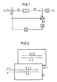
- the difference formation required for DPCM coding takes place according to FIG. 1 in a subtractor 2, the first input of which is connected to the input 1 and the second input of which is connected to a predictor 3.
- a recursive signal path is provided, which starts from a switching point 7 on the output side of the quantizer 4, contains a first adder 8, a limiter device 9 and the predictor 3 and is routed to the second input of the subtractor 2.
- the output of the predictor 3 is also connected to a second input of the first adder 8, which forms a so-called reconstructed pixel signal s R by adding the quantized difference signal ⁇ q and the prediction value ⁇ . For each current pixel signal s, the predictor 3 delivers the prediction value aus from at least one of the previous pixel signals
- the current image point lying in line n in a television picture m is designated by X
- the picture point scanned immediately before by A the picture point corresponding to X of the previous line n-1 by C and the one adjacent to the latter, immediately before or after this scanned picture elements with B and D and if the corresponding picture elements of the previous picture m - l are labeled with X 'and A' to D '
- the formation of the prediction value ⁇ for the picture element signal of X use the pixel signals from at least one of the points A to D, where one speaks of a two-dimensional (2D) prediction.
- the invention has for its object to provide a further arrangement for DPCM coding, in which fast signal processing is ensured with the simplest possible circuit structure. This is achieved according to the invention by designing the arrangement according to the characterizing part of patent claim 1.
- the advantage that can be achieved with the invention is, in particular, that a desired limiter function does not have to be arranged on the input side in a development of the invention and the arrangement in the development has the shortest possible critical path (a quantization for a DPCM system) handle, an addition and a register). If a limitation for the reconstructed value is required (such as in the COST specification for the ISDN broadband system), the critical path is only extended by an overflow detection and a multiplexer. It is also advantageous that, in contrast to systems that derive a similarly short critical path through recursive insertion into the prediction equation (see Figure 5 of the second publication mentioned on page 219), the value from the 2D or 3D prediction is only once is subtracted. The number of adders is less.
- the value range of the quantization error is smaller than the value range of the representative values.
- the memory required must therefore advantageously output fewer digits and is therefore smaller.
- the I / O expenditure is lower compared to conventional arrangements.
- Claims 2 to 11 are directed to preferred refinements and developments of the invention.
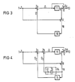
- the difference formation required for DPCM coding takes place in the first exemplary embodiment according to FIG. 3 as well as in the basic circuit diagram of the known arrangement according to FIG. 1 in a subtractor 2a, the first input of which is connected to input 1 of the DPCM circuit and the second input of which is a predictor 10 is connected. Instead of a quantizer, all difference signals or prediction errors are fed to a device for outputting a quantization error 11 associated with a difference signal. 3 has an additional adder 12, the first input of which is connected to the output of the last-mentioned arrangement and, via a second input, to the output of subtractor 2a.
- the quantized prediction error ⁇ q arises in that the associated quantization error q is added to the prediction error ⁇ at the output of the subtractor 2a.
- the output 13 of the further adder 12, which supplies the quantized prediction error ⁇ q, is connected to a transmission channel via an encoder (not shown).
- a recursive signal path is provided which starts from the output of the arrangement for outputting a quantization error 11 associated with a difference signal, contains a first adder 8 and a predictor 10 and is led to the second input of the subtractor 2a.
- the output of the first adder like the DPCM structure according to Figure 1, supplies a so-called reconstructed pixel signal s R. According to the known DPCM structure from FIG.
- this pixel signal s R arises from an addition of the prediction value ⁇ and the quantized prediction error ⁇ q.
- the second adder 8 is supplied with the quantization error q associated with a certain difference signal via the first input, and the current pixel signal s, which is on Input 1 is connected.
- the reconstructed pixel signal s R thus results from an addition of the pixel signal s and the quantization error q associated with the difference signal.
- the prediction and the Be Calculation of the prediction error ⁇ undergoes no change in the circuit according to the invention according to FIG. 3.
- the quantization error q is assigned to the prediction error ⁇ by a memory, a PLA or an arrangement of logic gates.
- the memory required for this generally has a smaller number of digits than the quantizer in the DPCM structure according to a conventional arrangement, since the large value range of the representative values is opposed by a smaller value range of associated quantization errors via the quantization characteristic.
- FIG. 4 shows a first development of the arrangement according to FIG. 3, in which the predictor has been divided into a 1D and 2D / 3D predictor 14, 15.
- the one-dimensional predictor 14 processes the immediately preceding value
- the two- or. three-dimensional predictor 15 processes all other values. These remaining values include, for example, the pixels of the previous line or the pixels of the previous image.
- the portions ⁇ 1, ⁇ 2 of the one-dimensional or two-dimensional / three-dimensional predictors are successively subtracted from the current pixel signal, so that a second subtractor 2b is required for this.
- This second subtractor 2b is connected between the first subtractor 2a and the device for outputting a quantization error 11 associated with a difference signal, so that the output of the first subtractor 2a with the first input of the second subtractor 2b and the output of the second subtractor 2b with the input the latter device 11 is connected.
- the second input of the second subtractor 2b is connected via the one-dimensional predictor 14 to the output of the first adder 8, so that the reconstructed pixel signal s R is present at the input of the one-dimensional predictor 14.
- the one-dimensional 4 is formed from a series connection of a register 16 and an evaluator 17, the evaluator 17 weighting the reconstructed pixel signal s R with the value ⁇ .
- the one-dimensional predictor 14 delays the reconstructed pixel signal s R by one clock and multiplies it by a weighting factor ⁇ . 4 corresponds to the DPCM structure according to FIG. 3, so that the quantizer 4 belonging to the prior art is replaced by a device for outputting a quantization error 11 associated with a difference signal with a downstream adder 12.
- FIG. 5 shows a second development of the DPCM structure according to FIG. 3. Since the reconstructed pixel signal s R is calculated from the addition of the current pixel signal s and the quantization error q associated with the difference signal, the one-dimensional predictor can again be divided into a first part 18 , which delays the current pixel signal s and multiplies it by the weighting factor ⁇ , and splits it into a second part 19, which delays the quantization error q associated with the difference signal and also multiplies it by the evaluation factor ⁇ . These two components ⁇ 1A , ⁇ 1B are also successively subtracted from the current pixel signal s, so that two additional subtractors 2b, 2c are required compared to the DPCM structure according to FIG. 3.
- An input of the second additional subtractor 2c is connected to the current pixel signal s, while a further input is connected to input 1 of the DPCM structure via the first part 18 of the one-dimensional predictor.
- the output of the last-mentioned subtractor 2c is at the first input of the first subtractor 2a and the output of the first subtractor 2a is at the first input of the third additional subtractor 2b and the output of this subtractor 2b is provided with the device for outputting a quantization error associated with a difference signal 11 connected.
- the second part 19 of the one-dimensional predictor is arranged.
- Both the first and the second part of the one-dimensional predictor consist of a series connection of a register (16 ⁇ , 16 'and a downstream evaluator 17 ⁇ , 17', which the current pixel signal s or the quantization error q associated with the difference signal with the weighting factor ⁇ multiplied).
- the rest of the interconnection, in particular of the 2D or of the 3D predictor and the device for outputting a quantization error 11 associated with a difference signal with the downstream adder 12 correspond to the DPCM structure according to FIG. 4.
- FIG. 6 A development of the DPCM structure according to the invention Fig. 5 with a shortest possible critical path is shown in Fig. 6.
- the predictor is divided into a 2D or 3D predictor 15 'and one 1D predictor, which consists of a first and second part 18 ', 19'.
- a further comparison with the last-mentioned DPCM structure shows that some registers have been arranged or supplemented elsewhere, whereas a register 24 from the line or image memory of the 2D or. 3D predictor was removed, which is indicated by the description with "-T".
- This measure makes it possible to build up the shortest possible critical path for a DPCM structure (a quantizer access, an addition and a register; provided the weighting factor ⁇ consists of a power of two and can therefore be realized by a bus shift that does not require computing time) a high processing speed of the DPCM structure ensures. Due to the change of the registers in the DPCM structure, it is also necessary to remove one register each in the input and output area in order to obtain the same function as in FIG. 5. If this is omitted, as shown here, the latency of the circuit, ie the time from the input of an input value to the output of the associated output value, is increased, but the function of the DPCM structure does not change.
- the structural structure in particular the arrangement of the first, second and third subtractors 2a, 2c, 2b, of first adder 8 and the device for outputting a quantization error 11 associated with a difference signal with a downstream adder 12 and the arrangement of the 2D or 3D predictor 15 'is similar to the DPCM structure according to FIG. 5, with the following exceptions.
- the first and second part 18 ', 19' of the one-dimensional predictor consists instead of a series connection of a register and an evaluator, only in both cases from an evaluator 17 ⁇ , 17 '.
- In the recursive signal path lies the 2D or 3D predictor 15 ', the line or image memory of which has been shortened by a register 24.
- a "T" register follows a 2D or 3D predictor l5 used in FIGS. 4 and 5.
- Further registers 20, 21 with respect to the DPCM structure according to FIG. 5 are reproduced between the first and second subtractors 2a, 2c and between the third subtractor 2b and the input of the device for outputting a quantization error 11 associated with a difference signal, while the signal path is also shown the current pixel signal to the second input of the first adder 8 is provided with a series connection of two registers 22, 23.
- the first part 18 'of the one-dimensional predictor is connected with its first connection between the two last-mentioned registers 22, 23 and with its second connection to the second input of the second subtractor 2c.
- FIG. 7 shows a development of the DPCM structure according to FIG. 6 with an additional register, which is arranged between the first and third subtractors 2a, 2b.
- This measure makes it possible to enable effective signal processing for the DPCM structure when the adders are slow compared to the memory access time. In general, however, this will not be necessary, since two cascaded additions run faster than one memory access plus one addition. Should it nevertheless be necessary to arrange a register 25 between the first and third subtractors 2a, 2b, then a further register 26 must also be provided for the second input of the first adder and the image or line memory of the 2D or. 3D predictor is closed by a total of two registers 24, 27 shorten.
- the basic arrangement of the DPCM structure according to FIG. 7 corresponds to the arrangement shown in FIG. 6, so that here too the shortest possible critical path, consisting of a quantizer access, an addition and a register, is present.
- the range of values of the reconstructed pixel signal must be limited.
- This limiting function can be installed in the manner shown in FIG. 8.
- the three states - below, within and above the value range - are recognized by an overflow detection.
- This overflow detection controls a multiplexer that selects between the three values - lower limit, unlimited value and upper limit.
- an arrangement according to FIG. 6 is again to be assumed, the arrangement shown additionally having an overflow detection 30, two multiplexers 28, 29 and three subtractors 33, 34, 35.
- the overflow detection 30 is connected to the output of the first adder 8 and controls the output of the first and second multiplexers 28, 29.
- Both multiplexers each have two inputs and one output, the first multiplexer 28 each having its first two inputs the lower or upper limit value G ⁇ , G+ is connected, and the third input is connected to the output of the first adder 8 together with the input of the overflow detection.
- the output of the first multiplexer 28, which carries the first reconstructed pixel signal s R is at the input of the 2D or. 3D predictor 15 'placed.
- the second multiplexer 29 has its first two inputs connected to the output of a fourth and fifth subtractor 34, 35, both inputs of the last-mentioned subtractor are connected in parallel and connected to the output of a sixth subtractor 33, the first connection of which to connection point 32 between the third and fourth registers 22, 23 and its second connection via the 2D or 3D predictor 15 'with the reconstructed pixel signal s R is applied.
- the 2D or The 3D predictor here again has a line or image memory, which is opposite by a register 24 the corresponding predictor arrangement from FIG. 3 is shortened.
- the maximum limit value G+ is switched via an evaluator 36 and multiplied by the weighting factor ⁇ with the aid of the evaluator 36, while the second input of the fifth subtractor 35 via a further evaluator 37 with the lower limit value G ⁇ Is connected and this evaluator also multiplies the lower limit by the weighting factor ⁇ .
- the third input of the second multiplexer 29 is connected to the output of the third subtractor 2b and the output of the same multiplexer 29 is connected to the input of the second register 21.
- the prediction error ⁇ results from the current pixel signal s minus the prediction value ⁇ 2 from the 2D / 3D predictor and minus the upper limit value G+ multiplied by ⁇ .
- the DPCM structure shown last like the DPCM structure according to FIGS. 6 and 7, has a shortest possible critical path, consisting of a quantizer access, an addition and a register. Thus, the highest possible processing speed is possible even in the last-mentioned arrangement.
Landscapes
- Engineering & Computer Science (AREA)
- Theoretical Computer Science (AREA)
- Multimedia (AREA)
- Signal Processing (AREA)
- Compression, Expansion, Code Conversion, And Decoders (AREA)
- Compression Or Coding Systems Of Tv Signals (AREA)
Applications Claiming Priority (2)
| Application Number | Priority Date | Filing Date | Title |
|---|---|---|---|
| DE3820234 | 1988-06-14 | ||
| DE3820234 | 1988-06-14 |
Publications (3)
| Publication Number | Publication Date |
|---|---|
| EP0346750A2 true EP0346750A2 (fr) | 1989-12-20 |
| EP0346750A3 EP0346750A3 (en) | 1990-07-25 |
| EP0346750B1 EP0346750B1 (fr) | 1993-06-09 |
Family
ID=6356527
Family Applications (1)
| Application Number | Title | Priority Date | Filing Date |
|---|---|---|---|
| EP89110290A Expired - Lifetime EP0346750B1 (fr) | 1988-06-14 | 1989-06-07 | Dispositif pour le codage par MICD avec un débit de données élevé |
Country Status (5)
| Country | Link |
|---|---|
| US (1) | US4893184A (fr) |
| EP (1) | EP0346750B1 (fr) |
| JP (1) | JPH0233288A (fr) |
| CA (1) | CA1312382C (fr) |
| DE (1) | DE58904598D1 (fr) |
Cited By (1)
| Publication number | Priority date | Publication date | Assignee | Title |
|---|---|---|---|---|
| RU2162280C2 (ru) * | 1993-10-13 | 2001-01-20 | Рка Томсон Лайсенсинг Корпорейшн | Устройство компрессии с дифференциальной импульсно-кодовой модуляцией |
Families Citing this family (5)
| Publication number | Priority date | Publication date | Assignee | Title |
|---|---|---|---|---|
| JPH0828875B2 (ja) * | 1989-08-21 | 1996-03-21 | 三菱電機株式会社 | 符号化装置および復号化装置 |
| JP3100447B2 (ja) * | 1992-01-10 | 2000-10-16 | 三菱電機株式会社 | 適応等化器および受信機 |
| DE4308417C1 (de) * | 1993-03-17 | 1994-09-15 | Deutsche Forsch Luft Raumfahrt | Verfahren zur Übertragung von Bildern mit niedriger Übertragungsbitrate |
| US7003605B2 (en) * | 2002-09-12 | 2006-02-21 | International Business Machines Corporation | Method and system for an improved differential form of transitional coding |
| US8654838B2 (en) | 2009-08-31 | 2014-02-18 | Nxp B.V. | System and method for video and graphic compression using multiple different compression techniques and compression error feedback |
Family Cites Families (3)
| Publication number | Priority date | Publication date | Assignee | Title |
|---|---|---|---|---|
| JPS62214792A (ja) * | 1986-03-14 | 1987-09-21 | Fujitsu Ltd | 差分符号化装置 |
| DE3679545D1 (de) * | 1986-04-19 | 1991-07-04 | Itt Ind Gmbh Deutsche | Datenreduzierschaltung mit einem differenz-pulscodemodulator fuer videosignale. |
| CA1334871C (fr) * | 1987-02-26 | 1995-03-21 | Norio Suzuki | Dispositif pour quantifier un signal de facon adaptative afin qu'un signal decode local ne sorte jamais de la dynamique du signal d'entree |
-
1989
- 1989-05-01 US US07/346,084 patent/US4893184A/en not_active Expired - Fee Related
- 1989-06-07 EP EP89110290A patent/EP0346750B1/fr not_active Expired - Lifetime
- 1989-06-07 DE DE8989110290T patent/DE58904598D1/de not_active Expired - Fee Related
- 1989-06-07 JP JP1145034A patent/JPH0233288A/ja active Pending
- 1989-06-12 CA CA000602481A patent/CA1312382C/fr not_active Expired - Fee Related
Cited By (1)
| Publication number | Priority date | Publication date | Assignee | Title |
|---|---|---|---|---|
| RU2162280C2 (ru) * | 1993-10-13 | 2001-01-20 | Рка Томсон Лайсенсинг Корпорейшн | Устройство компрессии с дифференциальной импульсно-кодовой модуляцией |
Also Published As
| Publication number | Publication date |
|---|---|
| JPH0233288A (ja) | 1990-02-02 |
| EP0346750B1 (fr) | 1993-06-09 |
| US4893184A (en) | 1990-01-09 |
| CA1312382C (fr) | 1993-01-05 |
| DE58904598D1 (de) | 1993-07-15 |
| EP0346750A3 (en) | 1990-07-25 |
Similar Documents
| Publication | Publication Date | Title |
|---|---|---|
| DE4302898C2 (de) | Arithmetische Recheneinheit mit Akkumulierfunktion | |
| EP0517324B1 (fr) | Appareil pour commander le quantificateur d'un codeur hybride | |
| DE69032548T2 (de) | Korrelationsberechnungseinrichtung | |
| DE4444304C2 (de) | Verfahren zum Erzeugen eines zusammengesetzten Videobildes | |
| EP0077089B1 (fr) | Dispositif pour stocker ou transmettre des signaux d'image codés par transformation et pour regagner ces signaux d'image | |
| DE3714589A1 (de) | Videosignal-codierer mit dpcm und adaptiver praediktion | |
| EP0346750B1 (fr) | Dispositif pour le codage par MICD avec un débit de données élevé | |
| EP0525900B1 (fr) | Circuit de filtrage pour le pré-traitement d'un signal vidéo | |
| DE2523625A1 (de) | Digitalfilter | |
| DE69130553T2 (de) | Arithmetisch logische Einheit | |
| DE3810916A1 (de) | Delta-pulscodemodulation | |
| DE3545106C2 (fr) | ||
| EP0144066B1 (fr) | Montage de circuit pour la détection rapide de la plus grande différence de trois valeurs numériques représentées | |
| DE69636352T2 (de) | Hierarchische Kodierungs-Vorrichtung und -Verfahren mit Speicher für ein digitales Bildsignal | |
| EP0288783B1 (fr) | Dispositif pour le codage DPCM de signaux de télévision | |
| EP0148528B1 (fr) | Méthode et circuit pour augmenter la résolution d'un signal digital dépendant du temps | |
| DE3326388C2 (fr) | ||
| DE69222626T2 (de) | Hochauflösendes Digitalfilter | |
| DE3621446A1 (de) | Geraet zum digitalen verarbeiten von kontinuierlichen bitstroemen | |
| DE3417139C2 (fr) | ||
| EP0197165B1 (fr) | Circuit de compression de données pour des signaux vidéo numériques avec un modulateur d'impulsions codées | |
| EP0241745A1 (fr) | Procédé de réduction de signaux d'images numériques par quantification de coefficients obtenus par une transformation orthonormale au moyen d'une matrice Hadamard symétrique quasi-cyclique | |
| DE69416592T2 (de) | Verfahren und vorrichtung zur bitmengenschätzung für einen kodierer mit variabler kodewortlänge | |
| EP0288782B1 (fr) | Dispositif pour le codage DPCM de signaux de télévision avec traitement rapide des signaux | |
| EP0346751B1 (fr) | Dispositif pour le codage en MICD de signaux de télévision |
Legal Events
| Date | Code | Title | Description |
|---|---|---|---|
| PUAI | Public reference made under article 153(3) epc to a published international application that has entered the european phase |
Free format text: ORIGINAL CODE: 0009012 |
|
| AK | Designated contracting states |
Kind code of ref document: A2 Designated state(s): DE FR GB IT |
|
| PUAL | Search report despatched |
Free format text: ORIGINAL CODE: 0009013 |
|
| AK | Designated contracting states |
Kind code of ref document: A3 Designated state(s): DE FR GB IT |
|
| 17P | Request for examination filed |
Effective date: 19901220 |
|
| 17Q | First examination report despatched |
Effective date: 19920917 |
|
| GRAA | (expected) grant |
Free format text: ORIGINAL CODE: 0009210 |
|
| AK | Designated contracting states |
Kind code of ref document: B1 Designated state(s): DE FR GB IT |
|
| REF | Corresponds to: |
Ref document number: 58904598 Country of ref document: DE Date of ref document: 19930715 |
|
| ITF | It: translation for a ep patent filed | ||
| GBT | Gb: translation of ep patent filed (gb section 77(6)(a)/1977) |
Effective date: 19930813 |
|
| ET | Fr: translation filed | ||
| PLBE | No opposition filed within time limit |
Free format text: ORIGINAL CODE: 0009261 |
|
| STAA | Information on the status of an ep patent application or granted ep patent |
Free format text: STATUS: NO OPPOSITION FILED WITHIN TIME LIMIT |
|
| 26N | No opposition filed | ||
| PGFP | Annual fee paid to national office [announced via postgrant information from national office to epo] |
Ref country code: DE Payment date: 19960819 Year of fee payment: 8 |
|
| PGFP | Annual fee paid to national office [announced via postgrant information from national office to epo] |
Ref country code: GB Payment date: 19970521 Year of fee payment: 9 |
|
| PGFP | Annual fee paid to national office [announced via postgrant information from national office to epo] |
Ref country code: FR Payment date: 19970626 Year of fee payment: 9 |
|
| PG25 | Lapsed in a contracting state [announced via postgrant information from national office to epo] |
Ref country code: DE Free format text: LAPSE BECAUSE OF NON-PAYMENT OF DUE FEES Effective date: 19980303 |
|
| PG25 | Lapsed in a contracting state [announced via postgrant information from national office to epo] |
Ref country code: GB Free format text: LAPSE BECAUSE OF NON-PAYMENT OF DUE FEES Effective date: 19980607 |
|
| GBPC | Gb: european patent ceased through non-payment of renewal fee |
Effective date: 19980607 |
|
| PG25 | Lapsed in a contracting state [announced via postgrant information from national office to epo] |
Ref country code: FR Free format text: LAPSE BECAUSE OF NON-PAYMENT OF DUE FEES Effective date: 19990226 |
|
| REG | Reference to a national code |
Ref country code: FR Ref legal event code: ST |
|
| PG25 | Lapsed in a contracting state [announced via postgrant information from national office to epo] |
Ref country code: IT Free format text: LAPSE BECAUSE OF NON-PAYMENT OF DUE FEES;WARNING: LAPSES OF ITALIAN PATENTS WITH EFFECTIVE DATE BEFORE 2007 MAY HAVE OCCURRED AT ANY TIME BEFORE 2007. THE CORRECT EFFECTIVE DATE MAY BE DIFFERENT FROM THE ONE RECORDED. Effective date: 20050607 |