EP0346596B1 - Optisches Modul mit angeschlossener Glasfaser - Google Patents
Optisches Modul mit angeschlossener Glasfaser Download PDFInfo
- Publication number
- EP0346596B1 EP0346596B1 EP89107185A EP89107185A EP0346596B1 EP 0346596 B1 EP0346596 B1 EP 0346596B1 EP 89107185 A EP89107185 A EP 89107185A EP 89107185 A EP89107185 A EP 89107185A EP 0346596 B1 EP0346596 B1 EP 0346596B1
- Authority
- EP
- European Patent Office
- Prior art keywords
- fiber
- optical
- support
- optical fiber
- solder
- Prior art date
- Legal status (The legal status is an assumption and is not a legal conclusion. Google has not performed a legal analysis and makes no representation as to the accuracy of the status listed.)
- Expired - Lifetime
Links
- 239000013307 optical fiber Substances 0.000 title claims description 36
- 230000003287 optical effect Effects 0.000 title claims description 22
- 239000000835 fiber Substances 0.000 claims description 47
- 229910000679 solder Inorganic materials 0.000 claims description 23
- 238000002844 melting Methods 0.000 claims description 6
- 230000008018 melting Effects 0.000 claims description 6
- 239000000758 substrate Substances 0.000 claims description 5
- 230000004907 flux Effects 0.000 claims description 4
- 238000000034 method Methods 0.000 claims description 4
- 238000007747 plating Methods 0.000 claims description 3
- 239000002184 metal Substances 0.000 description 7
- 229910052751 metal Inorganic materials 0.000 description 7
- 238000010438 heat treatment Methods 0.000 description 5
- 238000005476 soldering Methods 0.000 description 4
- 239000000919 ceramic Substances 0.000 description 2
- 229910015363 Au—Sn Inorganic materials 0.000 description 1
- ATJFFYVFTNAWJD-UHFFFAOYSA-N Tin Chemical compound [Sn] ATJFFYVFTNAWJD-UHFFFAOYSA-N 0.000 description 1
- 230000002411 adverse Effects 0.000 description 1
- 238000004891 communication Methods 0.000 description 1
- 238000011109 contamination Methods 0.000 description 1
- 230000008878 coupling Effects 0.000 description 1
- 238000010168 coupling process Methods 0.000 description 1
- 238000005859 coupling reaction Methods 0.000 description 1
- 239000006071 cream Substances 0.000 description 1
- 230000001419 dependent effect Effects 0.000 description 1
- -1 e.g. Substances 0.000 description 1
- 239000003365 glass fiber Substances 0.000 description 1
- PCHJSUWPFVWCPO-UHFFFAOYSA-N gold Chemical compound [Au] PCHJSUWPFVWCPO-UHFFFAOYSA-N 0.000 description 1
- 239000010931 gold Substances 0.000 description 1
- 229910052737 gold Inorganic materials 0.000 description 1
- 239000000463 material Substances 0.000 description 1
- 239000000155 melt Substances 0.000 description 1
- 238000012986 modification Methods 0.000 description 1
- 230000004048 modification Effects 0.000 description 1
- 230000005693 optoelectronics Effects 0.000 description 1
- 239000004065 semiconductor Substances 0.000 description 1
Images


Classifications
-
- G—PHYSICS
- G02—OPTICS
- G02B—OPTICAL ELEMENTS, SYSTEMS OR APPARATUS
- G02B6/00—Light guides; Structural details of arrangements comprising light guides and other optical elements, e.g. couplings
- G02B6/24—Coupling light guides
- G02B6/42—Coupling light guides with opto-electronic elements
- G02B6/4201—Packages, e.g. shape, construction, internal or external details
- G02B6/4202—Packages, e.g. shape, construction, internal or external details for coupling an active element with fibres without intermediate optical elements, e.g. fibres with plane ends, fibres with shaped ends, bundles
-
- G—PHYSICS
- G02—OPTICS
- G02B—OPTICAL ELEMENTS, SYSTEMS OR APPARATUS
- G02B6/00—Light guides; Structural details of arrangements comprising light guides and other optical elements, e.g. couplings
- G02B6/24—Coupling light guides
- G02B6/42—Coupling light guides with opto-electronic elements
- G02B6/4201—Packages, e.g. shape, construction, internal or external details
- G02B6/4219—Mechanical fixtures for holding or positioning the elements relative to each other in the couplings; Alignment methods for the elements, e.g. measuring or observing methods especially used therefor
- G02B6/4236—Fixing or mounting methods of the aligned elements
- G02B6/4238—Soldering
-
- G—PHYSICS
- G02—OPTICS
- G02B—OPTICAL ELEMENTS, SYSTEMS OR APPARATUS
- G02B6/00—Light guides; Structural details of arrangements comprising light guides and other optical elements, e.g. couplings
- G02B6/24—Coupling light guides
- G02B6/42—Coupling light guides with opto-electronic elements
- G02B6/4201—Packages, e.g. shape, construction, internal or external details
- G02B6/4248—Feed-through connections for the hermetical passage of fibres through a package wall
Definitions
- the invention relates to an optical module arrangement and a method of fixing an optical fiber to a fiber support as specified in the preambles of claims 1 and 6, respectively.
- Optical modules are used for example in optical communication systems, such as data links, optical local area networks (LANs) etc., wherein an optical fiber is to be connected to an optically operative device.
- optical communication systems such as data links, optical local area networks (LANs) etc.
- LANs local area networks
- optical module comprising an optically operative device, such as a semiconductor laser, a pin-photodiode and the like, and an optical fiber optically coupled to the optically operative device in a metal package.
- an optically operative device such as a semiconductor laser, a pin-photodiode and the like
- the end of an optical fiber inserted in the package is soldered to a fiber support in the package, and the fiber support is molded in one piece with the package.
- a problem with such structure is that when a change is made to the shape or location of the fiber support, a new mold including that of the package has to be prepared, and consequently such structure is unadjustable to changes.
- Another problem is that since the fiber support and the package are made of metal in one piece, the package adversely acts as a heat sink when the end of the optical fiber is soldered to the fiber support.
- EP-A-0 264 335 discloses an opto-electronic unit coupling a laser with an optical fiber and a method of aligning a laser with any optical fiber. Said unit is formed inside a metal package fitted with a tube for the optical fiber and several connections pins at the bottom thereof. To align the fiber with the laser a solder preform is melted, whereupon a drop of molten solder is deposited on the fiber supported by a metal block and the fiber's position is adjusted in three directions.
- FR-A-2 582 413 discloses an optical module arrangement and a method of fixing an optical fiber to a fiber support as specified in the preambles of claims 1 and 6, respectively, in which a solder preform is positioned over an optical fiber and melted with a view to hold the fiber in place. As the solder preform melting over the fiber can freely spread on a solder plate during a heating step performed by an electrical heating means a dislocation between the end face of the optical fiber and a laser optically coupled thereto can occur.
- main object of the present invention is to provide an optical module arrangement having a large scope for changes in shapes and locations of a fiber support and which enables an optical fiber to be soldered to a fiber support in a short period of time.
- optical fiber should be secured precisely with respect to an optically operative device and contamination by soldering flux should be prevented.
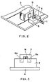
- a hybrid integrated circuit (IC) substrate 6 having a required circuit not shown. Openings are formed in side walls of the package 3. Through the openings an electric signal line 8 and an optical fiber 1 are inserted in the package 3.
- IC integrated circuit
- the optical fiber 1 is optically connected to a pin-photodiode not shown provided on a side of a carrier chip 2, and a light emitted from the end of the optical fiber 1 is incident on the light receiving portion of the pin-photodiode as a light receiving device.
- the optical fiber 1 has the end 1a made of so called metallised fiber which comprises exposed glass fiber and a plating applied thereto.
- the end 1a of the optical fiber 1 is first positioned precisely on a fiber support 5 disposed near the carrier chip 2 and then soldered to the fiber support 5.
- the hybrid IC substrate 6 is made of a heat insulative material, e.g., ceramics or others.
- the carrier chip 2 is mounted on the hybrid IC chip 6 as one element of the circuit.
- the fiber support 5 is made of metal or ceramics vacuum evaporated with metal and is beforehand plated with a solder.
- the fiber support 5 is die bonded to the hybrid IC substrate 6 with a solder having a relatively high melting point, e.g., gold and tin (Au-Sn) solder with a melting point of 280°C.
- the fiber support 5 After a cream solder is applied around the fiber support 5, the fiber support 5 is mounted on the hybrid IC substrate 6 and then heated. It is possible that the plating and die bonding of the fiber support 5 are performed simultaneously.
- the end 1a of the optical fiber 1 is positioned so as to be optically coupled connected to the pin-photodiode 9 on the front side wall of the carrier chip 2.
- Concavities 5a are formed on the top of the fiber support 5.
- the pre-formed structure 7 is made of a solder containing no flux and is shaped to have the form of a square bracket. It is preferable that the solder of the pre-formed structure 7 has lower melting point than that used to die bond the fiber support 5.
- the end 1a of the optical fiber 1 is plated beforehand to form a metallized fiber convenient for soldering.
- the pre-formed structure 7 and the fiber support 5 as arranged in the above described manner are heated. When the heating temperature exceeds above the melting point of the pre-formed structure 7, the pre-formed structure 7 melts. Then the heating is stopped. The melted pre-formed structure 7 cools and solidifies, and the end 1a of the optical fiber 1 is fixed to the fiber support 5.
- the end 1a of the optical fiber 1 may be positioned on the top of the fiber support 5 after the legs of the pre-formed structure 7 have been inserted and fixed in the concavities 5a and then the end 1a of the optical fiber 1 is put into the gap between the pre-formed structure 7 and the fiber support 5.
- the pre-formed structure 7 has a square bracket shape before melted but may have a U-shape or an L-shape as shown in Figs. 4 and 5.
- a top cover not shown is attached to the package to seal the optical module.
- the pre-formed structure 7 may have a J-shape in which the two legs have different lengths, and only one of the two legs is inserted in the concavity 5a. In this case there is only one concavity 5a.
- This embodiment forms an optical module comprising a pin-photodiode acting as a light receiving device, and an optical fiber optically coupled to the light receiving device.
- the optical module according to this invention could be a transmitting optical module wherein the light receiving device has been replaced by a light emitting diode or a laser diode acting as a light emitting device.
Landscapes
- Physics & Mathematics (AREA)
- General Physics & Mathematics (AREA)
- Optics & Photonics (AREA)
- Optical Couplings Of Light Guides (AREA)
Claims (6)
- Eine Anordnung eines optischen Moduls zum Erzeugen eines fertiggestellten optischen Moduls, wobei die Anordnung aufweist:- eine elektro-optische Einrichtung (9), die mit einer Optikfaser (1) optisch zu koppeln ist,- eine Optikfaserstütze (5) mit einer Abstützfläche, auf der die Faser (1) in richtiger Lage zu befestigen ist, wobei die Stütze nahe der elektro-optischen Einrichtung (9) vorgesehen ist, und- eine längliche Lötmittelvorform (7) mit vorbestimmter Gestalt, die über der Faser (1) angeordnet ist,dadurch gekennzeichnet,- daR die Optikfaserstütze (5) an einer vorbestimmten Stelle auf der Faserabstützfläche mit mindestens einer Vertiefung (5a) versehen ist, die ein entsprechendes Ende der Lötmittelvorform (7) aufnimmt und dadurch die Vorform über der Faser abstützt und ein brückenförmiges, über die Faser (1) hinüberführendes Element ausbildet, das nachfolgend geschmolzen werden kann, um die Faser (1) zum Befestigen zu umfassen.
- Eine Anordnung eines optischen Moduls nach Anspruch 1,
dadurch gekennzeichnet,- daR die Lötmittelvorform (7) eine J-förmige Gestalt aufweist, wobei eines der beiden Beine in die Vertiefung (5a) eingesetzt ist. - Eine Anordnung eines optischen Moduls nach Anspruch 1,
dadurch gekennzeichnet,- daß die Lötmittelvorform (7) die Gestalt einer eckigen Klammer, eine U-förmige Gestalt oder eine L-förmige Gestalt aufweist und- daß eine Vielzahl von Vertiefungen (5a, 5a) in der Faserabstützfläche vorgesehen ist, wobei die Beine der jeweiligen Lötmittelvorform darin eingesetzt sind. - Eine Anordnung eines optischen Moduls nach einem der vorhergehenden Ansprüche,
dadurch gekennzeichnet,- daß die Lötmittelvorform (7) kein Flußmittel enthält. - Eine Anordnung eines optischen Moduls nach einem der vorhergehenden Ansprüche,
dadurch gekennzeichnet,- daß die elektro-optische Einrichtung (9) zusammen mit der Faserstütze (5) auf einem wärmeisolierenden Substrat (6) befestigt ist. - Ein Verfahren zum Befestigen einer Optikfaser auf einer Abstützfläche einer Faserstütze, die in der Nähe einer elektro-optischen Einrichtung vorgesehen ist, einschließend die Schritte:(a) Positionieren der Optikfaser (1) auf der Abstützfläche der Faserstütze (5),(b) Positionieren einer vorbestimmten länglichen Lötmittelvorform (7) von vorbestimmter Gestalt über der Optikfaser (1) und(c) Aufschmelzen und Verfestigen der Lötmittelvorform (7) zum Umhüllen der Faser,gekennzeichnet durch die folgenden Schritte:(d) Beschichten der Abstützfläche der Faserstütze (5) mit einem Lötmittel vor dem Ausführen des Schrittes (a) und(e) Anordnen von zumindest einem Ende der Lötmittelvorform (7) in einer entsprechenden Vertiefung (5a) an einer vorbestimmten Stelle auf der Faserabstützfläche während des Ausführens des Schrittes (b), um dadurch die Vorform (7) über der Faser (1) zu halten und zu stützen und ein brückenförmiges, über die Faser (1) hinüberführendes Element auszubilden.
Applications Claiming Priority (4)
| Application Number | Priority Date | Filing Date | Title |
|---|---|---|---|
| JP10092888A JPH01270013A (ja) | 1988-04-22 | 1988-04-22 | 光ファイバ固定方法 |
| JP10092788A JPH01270012A (ja) | 1988-04-22 | 1988-04-22 | 光ファイバ固定台 |
| JP100927/88 | 1988-04-22 | ||
| JP100928/88 | 1988-04-22 |
Publications (3)
| Publication Number | Publication Date |
|---|---|
| EP0346596A2 EP0346596A2 (de) | 1989-12-20 |
| EP0346596A3 EP0346596A3 (en) | 1990-06-13 |
| EP0346596B1 true EP0346596B1 (de) | 1994-01-12 |
Family
ID=26441867
Family Applications (1)
| Application Number | Title | Priority Date | Filing Date |
|---|---|---|---|
| EP89107185A Expired - Lifetime EP0346596B1 (de) | 1988-04-22 | 1989-04-21 | Optisches Modul mit angeschlossener Glasfaser |
Country Status (4)
| Country | Link |
|---|---|
| US (1) | US4955683A (de) |
| EP (1) | EP0346596B1 (de) |
| CA (1) | CA1323227C (de) |
| DE (1) | DE68912206T2 (de) |
Families Citing this family (15)
| Publication number | Priority date | Publication date | Assignee | Title |
|---|---|---|---|---|
| US5155786A (en) * | 1991-04-29 | 1992-10-13 | International Business Machines Corporation | Apparatus and a method for an optical fiber interface |
| US5241614A (en) * | 1991-04-29 | 1993-08-31 | International Business Machines Corporation | Apparatus and a method for an optical fiber interface |
| GB2296101B (en) * | 1994-12-12 | 1998-04-01 | Northern Telecom Ltd | Optically coupling optical fibres to injection lasers |
| US5553182A (en) * | 1995-02-14 | 1996-09-03 | Mcdonnell Douglas Corporation | Alignment fixture and associated method for controllably positioning on optical fiber |
| US5606635A (en) * | 1995-06-07 | 1997-02-25 | Mcdonnell Douglas Corporation | Fiber optic connector having at least one microactuator for precisely aligning an optical fiber and an associated fabrication method |
| EP0927375B1 (de) * | 1995-06-07 | 2002-02-20 | McDonnell Douglas Corporation | Eine justiervorrichtung zum genauen ausrichten einer optischen faser und ein hiermit zusammenhängendes herstellungsverfahren |
| US5602955A (en) * | 1995-06-07 | 1997-02-11 | Mcdonnell Douglas Corporation | Microactuator for precisely aligning an optical fiber and an associated fabrication method |
| JPH10190141A (ja) * | 1996-12-20 | 1998-07-21 | Fujitsu Ltd | 光半導体モジュール |
| US6679636B1 (en) | 2001-06-29 | 2004-01-20 | Network Elements, Inc. | Method and apparatus for maintaining alignment of a laser diode with an optical fiber |
| US6671975B2 (en) * | 2001-12-10 | 2004-01-06 | C. William Hennessey | Parallel kinematic micromanipulator |
| US7410088B2 (en) * | 2003-09-05 | 2008-08-12 | Matsushita Electric Industrial, Co., Ltd. | Solder preform for low heat stress laser solder attachment |
| US7263260B2 (en) * | 2005-03-14 | 2007-08-28 | Matsushita Electric Industrial Co., Ltd. | Low cost, high precision multi-point optical component attachment |
| DE102008011525A1 (de) | 2008-02-27 | 2009-09-10 | Jenoptik Laserdiode Gmbh | Verfahren zur Herstellung einer Lichttransmissionsanordnung und Lichttransmissionsanordnung |
| WO2011122440A1 (ja) | 2010-03-30 | 2011-10-06 | 株式会社フジクラ | レーザ装置およびその製造方法 |
| CA2849459A1 (en) * | 2011-09-26 | 2013-04-04 | Alpha Metals, Inc. | Systems and methods for void reduction in a solder joint |
Family Cites Families (9)
| Publication number | Priority date | Publication date | Assignee | Title |
|---|---|---|---|---|
| JPS53128991A (en) * | 1977-04-15 | 1978-11-10 | Nec Corp | Coupler for optical semiconductor parts |
| US4296998A (en) * | 1979-12-17 | 1981-10-27 | Bell Telephone Laboratories, Incorporated | Encapsulated light source with coupled fiberguide |
| FR2503458A1 (fr) * | 1981-04-02 | 1982-10-08 | Cit Alcatel | Tete optique |
| FR2547661B1 (fr) * | 1983-06-14 | 1986-10-24 | Telecommunications Sa | Procede et dispositif de raccordement d'une fibre optique avec un detecteur photosensible et le procede de mise en oeuvre |
| JPS6173206A (ja) * | 1984-09-18 | 1986-04-15 | Hitachi Maxell Ltd | 磁気記録再生方式 |
| JPS61173205A (ja) * | 1985-01-29 | 1986-08-04 | Fujitsu Ltd | 光結合部の固定方法 |
| US4722586A (en) * | 1985-04-12 | 1988-02-02 | Tektronix, Inc. | Electro-optical transducer module |
| FR2582413B1 (fr) * | 1985-05-23 | 1988-12-02 | Comp Generale Electricite | Procede de couplage d'une fibre optique a un composant optoelectronique sur une embase |
| FR2605418B1 (fr) * | 1986-10-17 | 1990-04-20 | Thomson Semiconducteurs | Module pour le couplage entre un dispositif semi-conducteur et une fibre optique, et procede d'alignement de ce dispositif semi-conducteur et de cette fibre |
-
1989
- 1989-04-18 US US07/339,799 patent/US4955683A/en not_active Expired - Fee Related
- 1989-04-20 CA CA000597280A patent/CA1323227C/en not_active Expired - Fee Related
- 1989-04-21 DE DE68912206T patent/DE68912206T2/de not_active Expired - Fee Related
- 1989-04-21 EP EP89107185A patent/EP0346596B1/de not_active Expired - Lifetime
Also Published As
| Publication number | Publication date |
|---|---|
| US4955683A (en) | 1990-09-11 |
| DE68912206T2 (de) | 1994-08-04 |
| EP0346596A2 (de) | 1989-12-20 |
| EP0346596A3 (en) | 1990-06-13 |
| CA1323227C (en) | 1993-10-19 |
| DE68912206D1 (de) | 1994-02-24 |
Similar Documents
| Publication | Publication Date | Title |
|---|---|---|
| EP0346596B1 (de) | Optisches Modul mit angeschlossener Glasfaser | |
| US5647042A (en) | Optical link module connection system | |
| EP0196875B1 (de) | Montage für optisches Bauteil | |
| US5611013A (en) | Optical miniature capsule | |
| US4807956A (en) | Opto-electronic head for the coupling of a semi-conductor device with an optic fiber, and a method to align this semi-conductor device with this fiber | |
| US20050201666A1 (en) | Optical module, manufacturing method therefor, protective component, and protective component with electric wiring | |
| JPH06208037A (ja) | 光学パッケージ | |
| EP0439227B1 (de) | Halbleiteranordnung mit einem Träger, Verfahren zu seiner Herstellung, und Verfahren zum Herstellen des Trägers | |
| US7841781B2 (en) | Methods and apparatuses for providing a hermetic sealing system for an optical transceiver module | |
| US6151173A (en) | Assembly of optical components optically aligned and method for making this assembly | |
| US20090269075A1 (en) | Electro-optical assembly and method for making an electro-optical assembly | |
| EP0928026B1 (de) | Gegossenes Kunststoffgehäuse für ein Halbleiterbauelement | |
| US5469456A (en) | Laser device and method of manufacture using non-metalized fiber | |
| US7284913B2 (en) | Integrated fiber attach pad for optical package | |
| EP1570306B1 (de) | Verfahren und Vorrichtung zur Befestigung an optischen Fasern | |
| JP2002521847A (ja) | 光電子装置のリードフレームアタッチメント | |
| US7101092B2 (en) | Module having a circuit carrier and an electro-optical transducer and method for producing the same | |
| JPH0563769B2 (de) | ||
| JPH01302214A (ja) | チップキャリア | |
| US20040264886A1 (en) | Low cost package design for fiber coupled optical component | |
| WO2003096097A1 (en) | Small-formed optical module | |
| JP2864460B2 (ja) | 多心式光モジュール及びその製造方法 | |
| WO2002079812A2 (en) | Small-formed optical module | |
| JP2001523584A (ja) | 2つの構造をはんだビードを用いて組み立てる方法および該方法によって得られた組立体 | |
| JPH01270013A (ja) | 光ファイバ固定方法 |
Legal Events
| Date | Code | Title | Description |
|---|---|---|---|
| PUAI | Public reference made under article 153(3) epc to a published international application that has entered the european phase |
Free format text: ORIGINAL CODE: 0009012 |
|
| AK | Designated contracting states |
Kind code of ref document: A2 Designated state(s): DE FR GB SE |
|
| PUAL | Search report despatched |
Free format text: ORIGINAL CODE: 0009013 |
|
| AK | Designated contracting states |
Kind code of ref document: A3 Designated state(s): DE FR GB SE |
|
| 17P | Request for examination filed |
Effective date: 19901213 |
|
| 17Q | First examination report despatched |
Effective date: 19920630 |
|
| GRAA | (expected) grant |
Free format text: ORIGINAL CODE: 0009210 |
|
| AK | Designated contracting states |
Kind code of ref document: B1 Designated state(s): DE FR GB SE |
|
| REF | Corresponds to: |
Ref document number: 68912206 Country of ref document: DE Date of ref document: 19940224 |
|
| ET | Fr: translation filed | ||
| PLBE | No opposition filed within time limit |
Free format text: ORIGINAL CODE: 0009261 |
|
| STAA | Information on the status of an ep patent application or granted ep patent |
Free format text: STATUS: NO OPPOSITION FILED WITHIN TIME LIMIT |
|
| 26N | No opposition filed | ||
| EAL | Se: european patent in force in sweden |
Ref document number: 89107185.4 |
|
| PGFP | Annual fee paid to national office [announced via postgrant information from national office to epo] |
Ref country code: FR Payment date: 19960410 Year of fee payment: 8 |
|
| PGFP | Annual fee paid to national office [announced via postgrant information from national office to epo] |
Ref country code: GB Payment date: 19960412 Year of fee payment: 8 |
|
| PGFP | Annual fee paid to national office [announced via postgrant information from national office to epo] |
Ref country code: SE Payment date: 19960417 Year of fee payment: 8 |
|
| PGFP | Annual fee paid to national office [announced via postgrant information from national office to epo] |
Ref country code: DE Payment date: 19960429 Year of fee payment: 8 |
|
| PG25 | Lapsed in a contracting state [announced via postgrant information from national office to epo] |
Ref country code: GB Effective date: 19970421 |
|
| PG25 | Lapsed in a contracting state [announced via postgrant information from national office to epo] |
Ref country code: SE Effective date: 19970422 |
|
| GBPC | Gb: european patent ceased through non-payment of renewal fee |
Effective date: 19970421 |
|
| PG25 | Lapsed in a contracting state [announced via postgrant information from national office to epo] |
Ref country code: FR Free format text: LAPSE BECAUSE OF NON-PAYMENT OF DUE FEES Effective date: 19971231 |
|
| PG25 | Lapsed in a contracting state [announced via postgrant information from national office to epo] |
Ref country code: DE Free format text: LAPSE BECAUSE OF NON-PAYMENT OF DUE FEES Effective date: 19980101 |
|
| EUG | Se: european patent has lapsed |
Ref document number: 89107185.4 |
|
| REG | Reference to a national code |
Ref country code: FR Ref legal event code: ST |