EP0927375B1 - Eine justiervorrichtung zum genauen ausrichten einer optischen faser und ein hiermit zusammenhängendes herstellungsverfahren - Google Patents
Eine justiervorrichtung zum genauen ausrichten einer optischen faser und ein hiermit zusammenhängendes herstellungsverfahren Download PDFInfo
- Publication number
- EP0927375B1 EP0927375B1 EP96932310A EP96932310A EP0927375B1 EP 0927375 B1 EP0927375 B1 EP 0927375B1 EP 96932310 A EP96932310 A EP 96932310A EP 96932310 A EP96932310 A EP 96932310A EP 0927375 B1 EP0927375 B1 EP 0927375B1
- Authority
- EP
- European Patent Office
- Prior art keywords
- carrier
- alignment
- support structure
- optical fiber
- bimorphic
- Prior art date
- Legal status (The legal status is an assumption and is not a legal conclusion. Google has not performed a legal analysis and makes no representation as to the accuracy of the status listed.)
- Expired - Lifetime
Links
Images

Classifications
-
- G—PHYSICS
- G02—OPTICS
- G02B—OPTICAL ELEMENTS, SYSTEMS OR APPARATUS
- G02B6/00—Light guides; Structural details of arrangements comprising light guides and other optical elements, e.g. couplings
- G02B6/24—Coupling light guides
- G02B6/42—Coupling light guides with opto-electronic elements
- G02B6/4201—Packages, e.g. shape, construction, internal or external details
- G02B6/4219—Mechanical fixtures for holding or positioning the elements relative to each other in the couplings; Alignment methods for the elements, e.g. measuring or observing methods especially used therefor
- G02B6/422—Active alignment, i.e. moving the elements in response to the detected degree of coupling or position of the elements
- G02B6/4225—Active alignment, i.e. moving the elements in response to the detected degree of coupling or position of the elements by a direct measurement of the degree of coupling, e.g. the amount of light power coupled to the fibre or the opto-electronic element
-
- G—PHYSICS
- G02—OPTICS
- G02B—OPTICAL ELEMENTS, SYSTEMS OR APPARATUS
- G02B6/00—Light guides; Structural details of arrangements comprising light guides and other optical elements, e.g. couplings
- G02B6/24—Coupling light guides
- G02B6/26—Optical coupling means
- G02B6/32—Optical coupling means having lens focusing means positioned between opposed fibre ends
-
- G—PHYSICS
- G02—OPTICS
- G02B—OPTICAL ELEMENTS, SYSTEMS OR APPARATUS
- G02B6/00—Light guides; Structural details of arrangements comprising light guides and other optical elements, e.g. couplings
- G02B6/24—Coupling light guides
- G02B6/36—Mechanical coupling means
- G02B6/38—Mechanical coupling means having fibre to fibre mating means
- G02B6/3801—Permanent connections, i.e. wherein fibres are kept aligned by mechanical means
- G02B6/3803—Adjustment or alignment devices for alignment prior to splicing
-
- G—PHYSICS
- G02—OPTICS
- G02B—OPTICAL ELEMENTS, SYSTEMS OR APPARATUS
- G02B6/00—Light guides; Structural details of arrangements comprising light guides and other optical elements, e.g. couplings
- G02B6/24—Coupling light guides
- G02B6/42—Coupling light guides with opto-electronic elements
- G02B6/4201—Packages, e.g. shape, construction, internal or external details
- G02B6/4219—Mechanical fixtures for holding or positioning the elements relative to each other in the couplings; Alignment methods for the elements, e.g. measuring or observing methods especially used therefor
- G02B6/422—Active alignment, i.e. moving the elements in response to the detected degree of coupling or position of the elements
- G02B6/4226—Positioning means for moving the elements into alignment, e.g. alignment screws, deformation of the mount
-
- G—PHYSICS
- G02—OPTICS
- G02B—OPTICAL ELEMENTS, SYSTEMS OR APPARATUS
- G02B6/00—Light guides; Structural details of arrangements comprising light guides and other optical elements, e.g. couplings
- G02B6/24—Coupling light guides
- G02B6/36—Mechanical coupling means
- G02B6/3628—Mechanical coupling means for mounting fibres to supporting carriers
- G02B6/3648—Supporting carriers of a microbench type, i.e. with micromachined additional mechanical structures
- G02B6/3656—Supporting carriers of a microbench type, i.e. with micromachined additional mechanical structures the additional structures being micropositioning, with microactuating elements for fine adjustment, or restricting movement, into two dimensions, e.g. cantilevers, beams, tongues or bridges with associated MEMs
-
- G—PHYSICS
- G02—OPTICS
- G02B—OPTICAL ELEMENTS, SYSTEMS OR APPARATUS
- G02B6/00—Light guides; Structural details of arrangements comprising light guides and other optical elements, e.g. couplings
- G02B6/24—Coupling light guides
- G02B6/42—Coupling light guides with opto-electronic elements
- G02B6/4201—Packages, e.g. shape, construction, internal or external details
- G02B6/4219—Mechanical fixtures for holding or positioning the elements relative to each other in the couplings; Alignment methods for the elements, e.g. measuring or observing methods especially used therefor
- G02B6/4236—Fixing or mounting methods of the aligned elements
Definitions
- the present invention relates generally to methods and apparatus for controllably positioning an optical fiber and, more particularly, to an alignment apparatus for precisely aligning an optical fiber with an optical device and an associated fabrication method.
- optical fibers with an electro-optic device, such as a laser diode. Such alignment is particularly desirable in order to maximize the percentage of light coupled from the light source or electro-optic device to the optical fiber and to thereby increase the transmission efficiency of the optical signals.
- the alignment of optical fibers is complicated by the relatively small sizes of both the optical fiber waveguide, such as a single mode optical fiber which, for example, can have a light transmitting core diameter of approximately 2-10 micrometers, and the light source which has approximately the same size.
- an optical fiber generally has six degrees of freedom, each of which must be separately aligned.
- an optical fiber must generally be aligned in three translational directions, i.e., the X, Y and Z directions, and three rotational directions, i.e., ⁇ X , ⁇ Y and ⁇ Z .
- the alignment of polarization preserving or polarization maintaining optic fibers is complicated by the need to maintain the polarization axis of the optical fibers in alignment with that of the polarized optical system.
- individual metallized optical fibers can be soldered to a support.
- the solder bonding the metallized optical fiber to the support is generally heated to a temperature above the predetermined melting temperature of the solder. Thereafter, the optical fiber can be moved and, once the optical fiber is properly positioned, the solder can be allowed to cool and resolidify to fix the position of the optical fiber relative to the support and, more importantly, to a light source.
- These systems typically require, however, some means, such as solder, for retaining an optical fiber in place after the optical fiber has been positioned in a separate alignment process, distinct from the means for retaining the optical fiber in position.
- U.S. Patent No. 4,798,439 to Keith Preston (hereinafter the "'439 patent") describes an optical assembly and a related method for mounting optical components, such as an optical fiber, on a substrate.
- an optical fiber is lowered into a layer of solder, such as a solder preform or a solder paste, which has been applied to a submount assembly.
- a heating element is lowered into contact with the solder to locally melt the solder about the optical fiber such that the optical fiber can be mounted therein.
- a first end of the optical fiber is positioned to receive the output of a laser, also illustratively mounted on the submount assembly.
- the optical fiber By positioning the optical fiber such that the power level of the light transmitted through the optical fiber is maximized, the optical fiber is appropriately aligned with the laser. Once aligned, the heating element is cooled to allow the solder to solidify and to fix the optical fiber to the submount assembly.
- alignment and bonding systems may controllably position an individual optical fiber
- the heat required to allow one optical fiber to be positioned can oftentimes affect the position or alignment of adjacent optical fibers, thereby misaligning the adjacent optical fibers.
- these alignment and bonding systems and methods such as the systems disclosed by the '439 patent and the '796 patent, are generally relatively laborious and time-intensive, particularly, in instances in which a number of optical fibers must be individually aligned.
- Melles Griot has developed a system for precisely aligning optical fibers with other optical components.
- the Melles Griot alignment system generally includes a variety of relatively complex and costly components which significantly increase the fabrication costs to produce such precisely aligned optical devices.
- the optical fiber must generally be bonded with a separate bonding means, such as solder, as described in the foregoing patents.
- the Kaspar '354 patent describes a device for positioning an optical fiber that includes three pairs of elactromechanical deflector elements that are each arranged like a pair of leaf springs.
- the electromechanical deflectors are formed of a bilaminar ceramic.
- the deflectors Upon applying a suitable voltage to the deflectors, the deflectors will move in a predetermined displacement direction. Since the deflectors are operably connected to a pin that holds a respective optical fiber, movement of the deflectors also moves the optical fiber.
- Fiber optic connectors are commonly employed to align and to interconnect one or more optical fibers with a variety of optical devices or with other optical fibers.
- fiber optic connectors can be mounted on end portions of a pair of fiber optic cables, each of which include a number of optical fibers.
- the optical fibers of the fiber optic cables can, for example, transmit data or control signals between various remote devices, such as sensors or actuators, and a central control computer, such as a flight controller of an aircraft.
- the fiber optic connectors can then be interconnected such that the optical fibers of a first fiber optic cable are aligned with the optical fibers of a second fiber optic cable.
- the fiber optic connectors In order to efficiently transmit signals between optical fibers, the fiber optic connectors must precisely align the individual optical fibers such that the optical signals transmitted therethrough are efficiently coupled from fiber to fiber. Such alignment is particularly essential in connecting single mode optical fibers which must be precisely aligned with the light-transmitting core of another single mode optical fiber of similar size in order to efficiently transmit optical signals therethrough.
- a fiber optic connector In order to effectively couple optical signals from fiber to fiber, a fiber optic connector must maintain the precise alignment of the individual optical fibers in a predetermined manner such that the optical fibers will remain aligned as the fiber optic connecter is mated with another fiber optic connector or with other types of optical device. Therefore, a variety of methods as described above have been developed to align individual optical fibers prior to sealing the optical fibers within the fiber optic connector. Since fiber optic connectors typically include a plurality of optical fibers, all of which must be precisely aligned, the alignment process must generally be repeated for each optical fiber of the fiber optic connector prior to hermetically sealing the fiber optic connector.
- a fiber optic connector has been developed by AT&T Bell Laboratories and is described by R.J. Pimpinella in an article entitled " A New Type of Fiber Optic Connector Designed for Military Optical Backplanes ", published in the Proceedings of the 42nd ECTC Conference on May 18-20, 1992, pages A-6-1 through A-6-5.
- This fiber optic connector includes a silicon base which defines a v-groove.
- An optical fiber can be positioned within the v-groove and a ball lens can be disposed adjacent an end portion of the optical fiber to form an optical fiber sub-assembly.
- the optical fiber sub-assembly can be mated with a second optical fiber sub-assembly, also comprised of an optical fiber and a ball lens mounted to a silicon base, such that the optical signals transmitted by a first optical fiber are collimated by the pair of ball lenses so as to be efficiently coupled to the second optical fiber.
- the optical fiber sub-assemblies can be disposed within respective self-sealing connector enclosures.
- at least one of the connector assemblies has a spring-loaded cover that retracts upwardly to receive a corresponding portion of the other connector enclosure.
- the fiber optic connector disclosed by R.J. Pimpinella as well as the above-described alignment methods and systems do not provide for the precise alignment of one or more optical fibers within a hermetically sealed package, such as a hermetically sealed fiber optic connector. Instead, the retraction of the spring-loaded cover of the connector enclosure of the fiber optic connector disclosed by R.J. Pimpinella can allow contaminants or moisture to enter the connector enclosure.
- the fiber optic connector disclosed by R.J. Pimpinella does not provide for realignment of the optical fibers without replacing the silicon bases in which respective v-grooves are defined. Further, the fiber optic connector disclosed by R. J. Pimpinella is also relatively difficult due to the recessed areas adjacent the ball lens.
- the precise alignment of an optical fiber within a hermetically sealed package is complicated since, in addition to precisely aligning the optical fiber in each of the six degrees of freedom, the alignment process must typically be performed without physically contacting or otherwise heating the optical fiber since heat, such as body heat, can cause the optical fiber to move due to thermal expansion, thereby misaligning the optical fiber.
- access to an optical fiber within a hermetically sealed package is generally limited since the optical device with which the optical fiber is being aligned is disposed within an internal cavity defined within the hermetic package.
- the optical fiber can be precisely aligned with the optical device.
- the microactuator includes first and second bimorphic actuators for controllably positioning the carrier in first and second orthogonal directions, respectively, relative to the alignment support structure.
- the microactuator can also include a third bimorphic actuator for positioning the carrier in a third direction, orthogonal to the first and second directions. Accordingly, the carrier and the optical fiber mounted to the carrier can be controllably positioned in three orthogonal directions relative to the alignment support structure and, in turn, to the optical device.
- the first and second materials from which the bimorphic actuator is formed have first and second coefficients of thermal expansion, respectively.
- the bimorphic actuator can include a first layer of silicon and a second layer of a metallic material.
- the microactuator of this embodiment also includes current supply means for providing current to the bimorphic actuator such that the first and second materials differentially expand, thereby deflecting the respective bimorphic actuator.
- the second layer of the bimorphic actuator is formed of a piezoelectric material, such as PZT or PMN.
- the microactuator of this embodiment also includes voltage supply means for supplying voltage to the piezoelectric bimorphic actuator such that the bimorphic actuator deflects.
- the carrier can also include a carrier body to which the bimorphic actuator is affixed.
- each bimorphic actuator can include an elongate central portion extending between opposed end portions. The opposed end portions can be affixed to the carrier body such that the elongate central portion bends in response to electrical stimuli, such as current which induces differential expansion between the first and second layers.
- the alignment support structure includes means for securing the carrier to the alignment support structure once the optical fiber is aligned with the optical device.
- the alignment support structure includes at least one post formed, such as by a LIGA process involving a combination of lithography, electroforming and molding, so as to extend outwardly from the alignment support structure.
- the carrier can also define at least one aperture etched therethrough and adapted to receive a respective post therein.
- the aperture defined in the carrier can have a frustoconical shape to facilitate relative movement between the carrier and a respective post of the alignment support structure and can include an adhesive adapted to bond the outwardly extending post of the alignment support structure to the carrier once the optical fiber is precisely aligned with the optical device.
- the alignment support structure can include a recessed portion adapted to receive and hold an optical device, such as a laser diode.
- the alignment support structure can define a reference location and can include bias means for urging a predetermined portion of the carrier toward the reference location of the alignment support structure.
- the bias means includes a plurality of springs for contacting the carrier and for urging the predetermined portion of the carrier toward the reference location.
- the alignment support structure can also be comprised of a thermally conductive material for drawing heat from the optical device.
- the microactuator of the present invention precisely aligns an optical fiber with an optical device, such as a laser diode, due to the controlled deflection of the bimorphic actuators of the microactuator.
- the microactuator of the present invention does not heat or otherwise perturb adjacent microactuators or the optical fibers maintained therein such that a plurality of adjacent optical fibers can be precisely aligned.
- the microactuator of the present invention can precisely align an optical fiber with an optical device within a hermetically sealed package, such as a butterfly package.
- the microactuator of the present invention can be readily fabricated in an economical manner.
- the microactuator can remain within a hermetically sealed package to facilitate subsequent realignment or repositioning of the optical fiber.
- the microactuator can permanently bond an optical fiber in an aligned relationship with the optical device.
- the alignment apparatus includes a connector housing in which the alignment support structure and at least one microactuator are disposed.
- the fiber optic connector of this embodiment can efficiently couple the aligned optical fibers, such as single mode optical fibers, with other optical devices, including other optical fibers.
- the microactuator can be controllably positioned relative to the alignment support structure so as to precisely align the optical fiber mounted thereto after the connector housing has been hermetically sealed so as to further enhance the precision with which the optical fibers can be aligned.
- the connector housing of this advantageous embodiment preferably defines a plurality of apertures through which the optical signals are transmitted.
- This embodiment also preferably includes a plurality of optical fibers mounted to respective ones of a plurality of microactuators such that the optical fibers can be precisely aligned with respective apertures defined by the connector housing.
- the fiber optic connector housing also includes a plurality of lens elements, such as graded index lens elements, which are at least partially disposed within respective ones of the plurality of apertures defined by the connector housing.
- the microactuators can precisely align the plurality of optical fibers with respective ones of the plurality of lens elements such that the optical signals transmitted therethrough can be collimated.
- each lens element can include a metallized portion such that the lens elements can be affixed, such as by soldering, within the respective apertures.
- the alignment apparatus of this embodiment can precisely align one or more optical fibers, such as single mode optical fibers, with respective lens elements such that the optical signals transmitted by the optical fibers can be efficiently coupled to another optical device, such as another optical fiber.
- the microactuators can be disposed within the connector housing such that the optical fibers can be aligned with the respective lens elements without physically contacting the optical fiber and, in one advantageous embodiment, after the connector housing has been hermetically sealed such that the alignment of the optical fibers is further enhanced.
- Figure 1 is a perspective view illustrating a microactuator according to one embodiment of the present invention.
- Figure 2 is an exploded perspective view illustrating the microactuator of Figure 1 including the alignment support structure and the carrier in greater detail.
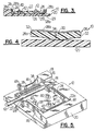
- Figure 3 is a cross-sectional view of the microactuator in one embodiment of the present invention taken along line 3-3 of Figure 1.
- Figure 4 is a cross-sectional view of a microactuator according to one embodiment of the present invention taken along line 4-4 of Figure 1.
- Figure 5 is a perspective view illustrating the deflection of a bimorphic actuator and the resulting movement of the carrier relative to the alignment support structure of the microactuator of one embodiment of the present invention.
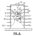
- Figure 6 is a schematic representation of the microactuator of one embodiment of the present invention disposed within a hermetically sealed package for aligning an optical fiber with an optical device which is also disposed within a hermetically sealed package.
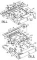
- Figure 7 is a front perspective view of a further embodiment of the present invention.
- Figure 8 is a rear perspective view of a fiber optic connector according to one embodiment of the present invention.
- Figure 9 is a perspective view of a pair of fiber optic connectors according to our embodiment of the present invention which have been mated in an aligned relation.
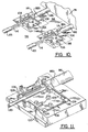
- Figure 10 is a fragmentary perspective view of a portion of the fiber optic connector of one embodiment of the present invention illustrating the substrate and a pair of microactuators mounted therein for aligning a pair of optical fibers with respective lens elements.
- Figure 11 is a greatly enlarged perspective view of a microactuator of one embodiment of the fiber optic connector of the present invention.
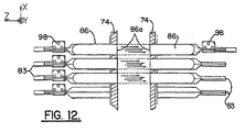
- Figure 12 is a schematic plan view illustrating the transmission of optical signals between the optical fibers of a pair of fiber optic connectors according to one embodiment of the present invention in which only a portion of the respective fiber optic connectors is illustrated for the sake of clarity.
- an alignment apparatus of the present invention includes a microactuator 10 for precisely aligning an optical fiber 12 with an optical device 14 is illustrated.
- the microactuator can align the optical fiber with an optical device, such as a laser diode, which is held within a corresponding recess 16 defined by the microactuator.
- the microactuator can precisely align an optical fiber with an external optical device, i.e., an optical device which is not mounted upon or otherwise held by the microactuator. In either instance, however, the microactuator is positioned in a fixed relation to the optical device.
- the alignment apparatus can be a fiber optic connector that includes one or more microactuators for aligning respective optical fibers, such as with the corresponding optical fibers of another fiber optic connector.
- the microactuator 10 can position various types of optical fibers 12 including multi-mode, single mode, and polarization preserving optical fibers.
- the microactuator of the present invention is particularly adapted to position single mode optical fibers in an aligned position since the microactuator can readily position optical fibers with the precision required to efficiently couple single mode optical fibers.
- the microactuator can align an optical fiber which includes a lensed facet.
- the microactuator can, alternatively, align an optical fiber having a cleaved end facet without departing from the spirit and scope of the present invention.
- the microactuator 10 typically includes an alignment support structure 20 , such as a substrate, as illustrated in Figures 1 and 2.
- the alignment support structure is disposed in a fixed relation to the optical device 14 .
- the alignment support structure can include a recessed portion 16 which is adapted to receive and hold the optical device.
- a laser diode can be disposed within the recessed portion defined by the alignment support structure.
- the alignment support structure of this embodiment can include a chamfered opening 18 so as to reduce or eliminate back reflections from the optical device.
- the alignment support structure 20 is preferably comprised of a thermally conductive material to serve as a heatsink for drawing heat from the optical device 14 as described hereinafter.
- the alignment support structure also draws heat from the carrier.
- the alignment support structure is comprised of a metallic material, such as copper or nickel.
- the alignment support structure 20 can be fabricated by a variety of processes as known to those skilled in the art.
- the alignment support structure can be electroformed, such as by a LIGA process, in order to obtain relatively large height-to-width ratios.
- the alignment support structure can include vertical sidewalls having precise tolerances.
- a LIGA process is based upon a combination of lithography, electroforming and molding.
- the acronym LIGA is derived from the German translation of lithography, electroforming and molding, namely, Lith driving, Galvanoformung and Abformung.
- the microactuator 10 also includes a carrier 22, movably mounted to the alignment support structure 20, for holding the optical fiber 12 in a fixed relation thereto.
- the carrier 22 preferably includes a carrier body 24 having an optical fiber holding means, such as a groove 26 defined in the carrier body, for receiving and holding the optical fiber in a fixed relation to the carrier body.
- the groove can be V-shaped and, in one embodiment, has opposed sidewalls which define an angle of 55° with respect to the surface of the carrier body.
- the groove can have a variety of other cross-sectional shapes without departing from the spirit and scope of the present invention.
- the carrier 22 is comprised of silicon.
- the V-shaped groove 26 can be formed by anisotropically wet etching the carrier body.
- the carrier can be comprised of other materials, such as metallic materials, without departing from the spirit and scope of the present invention.
- the carrier can be coated with a material having a relatively low coefficient of friction, such as a TEFLON® coating.
- the V-shaped groove 26 preferably has a predetermined depth such that the optical fiber 12 will initially be held slightly below, such as 5 ⁇ m below, the final aligned position of the optical fiber.
- the microactuator 10 can controllably adjust the position of the optical fiber upwardly and into alignment with the optical device 14 as described hereinafter.
- the groove can be formed so as to initially hold the optical fiber in other predetermined relationships to the final aligned position of the optical fiber without departing from the spirit and scope of the present invention.
- the optical fiber is preferably bonded within the groove 26 .
- the optical fiber can be bonded to the carrier with an optical fiber bonding agent, such as Gould GlasSolderTM bonding agent, or a high temperature fluxless solder, such as gold/tin eutectic alloy solder.
- the optical fiber is also preferably metallized, such as with titanium, platinum and gold, in order to be securely bonded within the groove.
- the microactuator 10 of the present invention also includes positioning means for controllably positioning the carrier 22 relative to the alignment support structure 20 such that the optical fiber 12 is, in turn, precisely aligned with the optical device 14 .
- the carrier includes the positioning means which can include at least one bimorphic actuator 28, such as a BIMORPH® element manufactured by Morgan Matroc, Inc..
- the carrier includes three bimorphic actuators which are adapted to controllably position the carrier in three orthogonal directions relative to the alignment support structure.
- each bimorphic actuator 28 is preferably comprised of first and second layers 28a and 28b .
- the first and second layers are formed of first and second materials, respectively, which respond differently to electrical stimuli.
- the bimorphic actuator will deflect in a predetermined direction by a controllable amount.
- the amount of the deflection of the bimorphic actuator will be proportional to the magnitude of the electrical stimulation.
- Each bimorphic actuator 28 generally includes an elongate central portion 30 extending between opposed end portions 32 as shown in Figure 4.
- the opposed end portions can be affixed to the carrier body 24 while the elongate central portion is separated from the carrier body as shown in Figure 3.
- the opposed end portions can be disposed within slots defined by the carrier body to thereby permit limited relative movement between the opposed end portions and the carrier body.
- the elongate central portion of the bimorphic actuator will bend in a predetermined direction, such as downwardly as shown in Figure 5 and as indicated by arrow 34 in Figure 4.
- the bimorphic actuator Upon bending in the predetermined direction, the bimorphic actuator is urged against the alignment support structure 20 so as to apply an oppositely directed force to the carrier 22 , thereby moving the carrier relative to the alignment support structure. Accordingly, the carrier can be controllably positioned relative to the alignment support structure such that the optical fiber 12 bonded to the carrier is precisely aligned with the optical device 1 4.
- the microactuator 10 of one advantageous embodiment includes three orthogonally positioned bimorphic actuators 28 adapted to move the carrier 22 in three orthogonal directions, namely, the x, y and z directions as designated for purposes of illustration in Figure 1, relative to the alignment support structure 20 .
- the carrier and, in turn, the optical fiber 12 bonded thereto can be controllably positioned in each of the three orthogonal directions.
- the rotational alignment of the optical fiber with the optical device 14 is provided by the precise formation of the groove 26 relative to the recessed portion 18 of the alignment support structure which holds the optical device.
- the first and second layers 28a and 28b of each of the bimorphic actuators 28 are comprised of first and second materials, respectively.
- the first and second materials of this embodiment are selected to have first and second coefficients of thermal expansion, respectively.
- the first material can be silicon while the second material is a metal, such as nickel or copper, having a larger coefficient of thermal expansion than the first material.
- the metallic second layer can be deposited on the first layer by a variety of methods, including preferential sputtering, directed evaporation and electroplating, without departing from the spirit and scope of the present invention.
- the microactuator 10 also includes current supply means for providing current to the bimorphic actuator 28 to resistively heat the bimorphic actuator such that the first and second materials of the first and second layers, respectively, differentially expand, thereby deflecting the bimorphic actuator.
- current supply means for providing current to the bimorphic actuator 28 to resistively heat the bimorphic actuator such that the first and second materials of the first and second layers, respectively, differentially expand, thereby deflecting the bimorphic actuator.
- bonding pads typically comprised of a conductive material, such as gold, are formed on the opposed end portions 32 of the bimorphic actuators such that an electrical current can be established therebetween.
- the elongate central portions 30 of the bimorphic actuators bend downwardly and outwardly as shown in Figure 5.
- the elongate central portions of the first and second bimorphic actuators i.e., the x- and z-bimorphic actuators, are therefore urged against respective sidewalls of the alignment support structure 20 such that the carrier 22 is moved in a direction away from the sidewalls in response thereto as indicated by arrows 36 in Figure 5.
- the elongate central portion of the third bimorphic actuator i.e., the y-bimorphic actuator
- the elongate central portion is urged downwardly against the alignment support structure such that the carrier is moved upwardly in response thereto as shown in Figures 4 and 5.
- the elongate central portion is preferably separated from the remainder of the carrier body 24 by relief grooves 29 defined laterally alongside the elongate central portion as best shown in Figure 3 which allow the bimorphic actuator to flex.
- the amount of the bending or deflection and, consequently, the position of the carrier relative to the alignment support structure can be controlled since the amount of bending is generally proportional to the current supplied to the individual bimorphic actuators.
- a bimorphic actuator 28 having a first layer 28a comprised of a highly doped semiconductor material, such as highly doped silicon, can also be heated by introducing current to the highly doped semiconductor material.
- the bimorphic actuator By introducing current to a first layer comprised of a highly doped semiconductor material, the bimorphic actuator can be resistively heated such that the first and second layers differentially expand, thereby deflecting the bimorphic actuator.
- sufficient resistive heating can generally be provided by relatively small amounts of the current, such as 10 mA, thereby reducing the power requirements for the microactuator 10 of this embodiment.
- the bimorphic actuator can include an additional layer comprised of a material having a greater resistance than that of the metallic second layer.
- the bimorphic actuator of this embodiment can also include an insulating layer, such as a layer of silicon dioxide, disposed between the metallic second layer and the additional layer having a greater resistance.
- each bimorphic actuator 28 includes a second layer 28b of an electrostrictive or piezoelectric material which, as known to those skilled in the art, will controllably move or deflect upon the application of a voltage thereto.
- the microactuator 10 of this embodiment also includes voltage supply means for providing a voltage to the bimorphic actuator such that the bimorphic actuator controllably deflects.
- the bimorphic actuator includes a first layer 28a comprised of silicon and a second layer comprised of a piezoelectric material, such as PZT or PMN.
- the amount of deflection or bending of the bimorphic actuator and, consequently, the position of the carrier 22 relative to the alignment support structure 20 can likewise be controlled.
- bonding pads are preferably disposed on the opposed end portions 32 of the bimorphic actuator such that a predetermined voltage can be established therebetween.
- the microactuator 10 of the present invention can align an optical fiber 12 with an optical device 14 by controllably varying the deflection of the respective bimorphic actuators 28.
- the efficiency with which the optical signals produced by the optical device are coupled to and transmitted via the optical fiber can be detected.
- the optical fiber can be held in position by the bimorphic actuators while the relative positions of the carrier 22 and the alignment support structure 20 are fixed, such as by bonding the carrier to the alignment support structure.
- the alignment support structure 20 includes means for securing the carrier 22 thereto once the optical fiber 12 is aligned with the optical device 14 .
- the securing means can include at least one outwardly extending post 40 which is preferably formed by a LIGA process.
- the carrier of this embodiment preferably defines at least one aperture 42 adapted to receive a respective post therein.
- the apertures defined by the carrier are preferably anisotropically wet-etched or laser cut therein and, in one embodiment, are frustoconical in shape so as to facilitate movement between the carrier and the post of the alignment support structure.
- the groove 26 and the apertures 42 are preferably anisotropically etched in the carrier 22 in two different directions or orientations, such as ⁇ 110> and ⁇ 100>.
- the carrier can be comprised of at least two different wafers, such as silicon wafers, having different orientations, such as ⁇ 110> and ⁇ 100> in the above example.
- the carrier can be coated with a material having a relatively low coefficient, such as a TEFLON® coating, in order to reduce the frictional forces between the carrier and the alignment support structure 20 .
- the securing means of the alignment support structure 20 can also include an adhesive adapted to bond the outwardly extending posts 40 of the alignment support structure to the carrier 22 once the optical fiber 12 is precisely aligned with the optical device 14.
- an adhesive adapted to bond the outwardly extending posts 40 of the alignment support structure to the carrier 22 once the optical fiber 12 is precisely aligned with the optical device 14.
- a bonding agent such as gold/tin eutectic alloy solder, a Gould GlasSolderTM bonding agent or glass frit, can be disposed on the interior surface of the aperture defined by the carrier.
- the adhesive can be activated, such as by laser heating or resistive heating, to bond the carrier to the alignment support structure. Once the alignment support structure and the carrier are bonded, the alignment of the optical fiber with the optical device is maintained irrespective of further electrical stimulation of the bimorphic actuators 28.
- the microactuator 10 and, more preferably, the alignment support structure 20 can define a reference location 44 with which a predetermined portion of the carrier 22, such as a predetermined corner 22a , is preferably initially positioned. Thereafter, the position of the carrier can be adjusted relative to the alignment support structure such that the optical fiber 12 is precisely aligned with the optical device 14 .
- the carrier 22 can be initially positioned relative to the alignment support structure 20 such that the optical fiber 12 is slightly misaligned, such as by 5-10 micrometers, relative to the optical device in a predetermined direction.
- the predetermined direction is preferably selected based upon the relative movement provided by the bimorphic actuators 28 such that the bimorphic actuators can compensate for the slight misalignment and can align the optical fiber with the optical device.
- the bimorphic actuators of the microactuator 10 are generally designed to move the carrier, and, in turn, the optical fiber in a predetermined direction, typically one predetermined direction, relative to the alignment support structure as illustrated by arrows 34 and 36 in Figures 4 and 5.
- the carrier is preferably initially positioned so as to be slightly misaligned in a direction opposite that indicated by arrows 34 and 36 such that movement of the carrier in the predetermined direction by the bimorphic actuators compensates for the slight misalignment and, in fact, brings the optical fiber into alignment with the optical device.
- the alignment support structure 20 also includes bias means for urging the predetermined portion of the carrier 22 towards the reference location 44 defined by the alignment support structure.
- the bias means includes a plurality of springs 46 for contacting the carrier, such as a sidewall 38 of the carrier, and for urging the predetermined portion of the carrier toward the reference location.
- the alignment support structure of the illustrated embodiment includes first and second springs for urging the carrier in first and second orthogonal directions, respectively, toward the reference location.
- the first and second springs 46 preferably urge the carrier 22 in first and second directions, respectively, which are substantially opposite to the first and second directions in which the first and second bimorphic actuators 28 , i.e., the x- and z-bimorphic actuators, urge the carrier.
- the bias force provided by the springs is preferably less than the force provided by the bimorphic actuators upon deflection, however, such that deflection of the bimorphic actuators overcomes the bias force of the springs and frictional forces between the carrier and the alignment support structure 20 so as to move the predetermined portion of the carrier away from the reference location 44 .
- the springs 46 can also be formed during a LIGA process so as to have relatively large height-to-width ratios.
- the springs can include a curved or hook member 48 to facilitate opening or spreading of the springs upon mounting of the carrier 22 to the alignment support structure 20 .
- a microprobe can engage a respective hook member so as to open or spread the spring during mounting of the carrier.
- the microactuator 10 of the present invention can controllably align an optical fiber 12 with an optical device 14 , such as a laser diode, within a hermetically sealed package, such as a hermetically sealed butterfly package.
- the microactuator can align the optical fiber with the optical device prior to or following the hermetic sealing of the package. If the optical fibers are aligned prior to hermetically sealing the package, the package can thereafter be potted, such as with a plastic material, or a lid may be affixed to the package, such as by laser welding or seam sealing, such that the package housing the aligned optical fibers is hermetically sealed.
- the hermetically sealed package typically includes a hermetic canister 50, such as a gold-plated KOVARTM canister having a plurality of KOVARTM feed-through pins 52 which are glass-to-metal hermetically sealed to the canister.
- An optical device 14 and a microactuator 10 having an optical fiber 12 mounted thereto are also disposed within the hermetic canister.
- the optical fiber is preferably metallized and soldered to the fiber optic sealing tube 54 of the hermetic canister.
- the hermetically sealed package can also include means for controlling the temperature of the optical device including a thermistor 56 and a thermal electric cooler 58 .
- the hermetically sealed package can include a photodetector 60 for detecting the output of the optical device such that the excitation energy supplied to the optical device and the resulting output of the optical device can be controlled as desired, such as controlling the excitation energy supplied to the optical device such that a constant output is provided by the optical device.
- the optical fiber 12 is preferably aligned with the optical device 14 with the microactuator 10 within the hermetic canister 50 as described above.
- the bimorphic actuators 28 of the microactuator, as well as the other electrical components disposed within the hermetic canister, are electrically stimulated, such as by leads 56 extending from respective pins 52 of the hermetically sealed package as illustrated in Figure 6.
- the alignment of the optical fiber to the optical device can be controlled.
- the first, second and third bimorphic actuators can be controllably adjusted in three orthogonal directions by providing appropriate electrical stimulation via the leads identified as X, Y and Z in Figure 6.
- the optical fiber can be precisely aligned with the optical device.
- the relative positions of the optical fiber 12 and the optical device 14 can be fixed by bonding the carrier 22 to the alignment support structure 20 , such as by heating the adhesive disposed within the respective apertures 42 defined by the carrier.
- the hermetic canister 50 can include a transparent window through which a laser can be directed so as to heat the adhesive and bond the carrier to the alignment support structure.
- the hermetically sealed package can include an additional lead which is electrically connected to the alignment support structure in the vicinity of the adhesive such that the adhesive can be resistively heated and the carrier can thereby be bonded to the alignment support structure.
- an optical fiber 12 can be precisely aligned with an optical device 14 , such as a laser diode, within a hermetically sealed package.
- an optical device 14 such as a laser diode
- the respective positions of the optical fiber and the optical device can be fixed such that the precise alignment is maintained.
- the microactuator can thereafter remain within the hermetically sealed package following the alignment of the optical fiber with the optical device, thereby further insuring that the optical fiber maintains alignment with the optical device.
- the microactuator can subsequently reposition or realign the optical fiber with the optical device to compensate for variations in the optical alignment which occur during use.
- one or more microactuators 98 can be disposed within a fiber optic connector 70 .
- the microactuators can precisely align optical fibers 83 with respective lens elements 86 of the fiber optic connector in order to collimate the optical signals transmitted therethrough.
- the alignment apparatus of the embodiment illustrated in Figure 7 includes a connector housing 72.
- the connector housing can be comprised of a variety of materials
- the connector housing of one embodiment is comprised of a metal, such as stainless steel, and, in a more specific embodiment, is comprised of KOVARTM brand stainless steel.
- a KOVARTM connector housing is comprised of a type of stainless steel which has a coefficient of thermal expansion which matches the coefficient of an optical fiber and thermal expansion of a glass lens element, an optical fiber and the glass of the glass-to-metal seals or bonds, such as between the lens elements and the front plate 74 of the fiber optic connector, as known to those skilled in the art.
- the connector housing 72 can include a face plate 74 defining a plurality of apertures 76 therethrough.
- the face plate is mounted to the cup-shaped body portion 78 of the connector housing as shown in Figure 7 to thereby define an internal cavity within the connector housing.
- the face plate can be laser welded or seam sealed to the body portion such that the connector housing is hermetically sealed.
- the exterior surface of the front plate can be polished so as to form a relatively planar surface, including the lens elements and the front plate, such that the front plate is more readily cleanable and can be coated, such as with an anti-reflection coating. By polishing the front plate, spurious deflections from surface defects on the front plate can also be minimized.
- the front plate can be polished at a predetermined angle, such as 3° to 5°, to prevent light reflections from the respective front plates of a pair of mated fiber optic connectors, thereby minimizing reflected feedback.
- the rear surface of the connector housing 72 can include a slot 81 through which one or more optical fibers 83 extend.
- a fiber optic cable 84 such as a fiber optic ribbon cable, comprised of a plurality of individual optical fibers can extend through the slot defined in the rear surface of the connector housing.
- each of the optical fibers is preferably individually aligned with a respective aperture 76 defined in the front plate 74 of the connector housing.
- the fiber optic connector 70 of the present invention can include one or more lens elements 86.
- a lens element is disposed within each of the apertures 76 defined in the front plate 74 of the connector housing 72 for collimating the optical signals transmitted by the respective optical fibers.
- At least a portion of each lens element is preferably metallized, such as with titanium, platinum and gold, such that the lens elements can be affixed, such as by soldering, within the respective apertures defined in the front plate of the connector housing.
- an end portion 86a of each lens element is polished, coated with an anti-reflection coating and aligned with the polished exterior surface of the front plate of the connector housing as illustrated in Figure 7.
- the lens elements can also include cylindrical graded index lens elements to further enhance the collimation of the optical signals.
- the alignment apparatus of the present invention can precisely align a plurality of optical fibers 83 with respective ones of a plurality of lens elements 86 disposed within the respective apertures 76 defined in the front plate 74 of the connector housing 72 .
- the fiber optic connector can then be mated with a second fiber optic connector, such that the optical signals transmitted via the optical fibers of the first fiber optic connector can be efficiently coupled to the optical fibers of the second fiber optic connector.
- one of the fiber optic connectors can include a plurality of alignment pins 88 extending outwardly from the front plate 74 as shown in Figure 7.
- the front plate of the other fiber optic connector can define a plurality of corresponding apertures adapted to receive respective ones of the alignment pins.
- the alignment apparatus of the present invention includes an alignment support structure or a substrate 96 , such as a metallic, a ceramic or a silicon substrate, and at least one microactuator 98 mounted on the substrate and adapted from relative movement therewith.
- An optical fiber 83 is preferably affixed to each microactuator such that the relative movement of the microactuator will controllably position the respective optical fiber with respect to an aperture 76 defined in the front plate 74 of the connector housing 72 and, in one advantageous embodiment, with respect to a lens element 86 disposed within the aperture.
- one advantageous embodiment includes a plurality of microactuators, one of which is associated with each optical fiber so as to align the respective optical fiber with a corresponding lens element 86.
- each microactuator 98 of this embodiment operates in a similar manner to that described above.
- each microactuator includes positioning means, such as one or more bimorphic actuators 106 , for controllably positioning the carrier 100 relative to the substrate 96 .
- the substrate can define a plurality of recessed portions in which the respective microactuators are disposed.
- the bimorphic actuators of the microactuators are preferably urged against the surrounding sidewalls of the substrate upon electrical stimulation of the bimorphic actuator such that the optical fibers carried by the microactuators can be controllably positioned relative to a respective lens element 86 .
- the microactuator 98 of this embodiment of the present invention can thereby align an optical fiber 83 with a respective lens element 86 by controllably varying the deflection of the respective bimorphic actuators 106 .
- the efficiency with which the optical signals produced by the optical device are coupled to and transmitted via the optical fiber can be detected.
- the optical fiber can be held in position by the bimorphic actuators while the relative positions of the optical fibers and the lens elements are fixed.
- the substrate 96 can also include one or more sets of first and second grooves 114 .
- the first and second grooves are sized and shaped for receiving an optical fiber 83 and a lens element 86 , respectively.
- the lens element can include a hemispherically ground surface on a first end 86b and a polished second end 86a to further facilitate the collimation and transmission of optical signals so as to reduce, among other things, spurious reflections.
- both end surfaces of the lens element, as well as the end surface of the optical fiber can be coated with an anti-reflectant coating to further enhance optical transmission.
- each optical fiber 83 received by the fiber optic connector 70 is preferably disposed within a respective groove 114 defined in the substrate 96 .
- a microactuator 98 and a lens element 86 are also associated with each optical fiber such that the microactuator can controllably position the respective optical fiber with the lens element.
- the lens elements collimate the optical signals.
- a plurality of microactuators 98 can be mounted on a substrate 96 within the internal cavity of the connector housing 72 .
- An optical fiber 83 is also preferably bonded to the carrier 100 of each microactuator such that the microactuators can controllably position the optical fibers with respect to respective lens elements 86 disposed within apertures 76 defined in the front plate 74 of the connector housing 72 . Since the microactuators and the optical fibers mounted thereon need not be physically contacted during the alignment process, the optical fibers can be aligned either prior to or following the hermetic sealing of the connector housing, such as by affixing the front plate thereto.
- the optical fibers 83 are aligned prior to sealing the connector housing 72 , the optical fibers can be aligned with respect to respective lens elements. Thereafter, the connector housing can be sealed. For example, a lid can be secured, such as by seam sealing, to the connector housing following alignment of the optical fibers.
- the relative positions of the optical fibers can be fixed prior to sealing the connector housing, such as by activating an adhesive between the carrier 100 and the substrate 96 as described below, thereby bonding the carrier to the substrate.
- the fiber optic connector 70 can also include a plurality of electrical pins 116 which can, in one embodiment, extend through the rear surface 82 of the connector housing to provide electrical access to the bimorphic actuators 106 of the plurality of microactuators 98 .
- electrical leads preferably interconnect the pins with respective ones of the bimorphic actuators and, more particularly, with bonding pads disposed on the opposed end portions 109 of each bimorphic actuator. Accordingly, by applying appropriate electrical stimuli to predetermined ones of the electrical pins, each optical fiber can be individually positioned in first, second and third orthogonal directions relative to the respective lens element 86 after the connector housing has been hermetically sealed.
- the relative alignment of the optical fiber with a respective lens element can be determined.
- the position of the optical fiber at which the maximum output power is detected can be determined.
- the end surface of the optical fiber is preferably aligned at the focal point of the respective lens element.
- the relative positions of the optical fiber 83 and the lens element 86 can be fixed by bonding the carrier 100 to the substrate 96 , as described above, such as by heating the adhesive disposed within the respective apertures 112 defined by the carrier such that the position of the carrier relative to the substrate which provides the maximum output power remains fixed.
- the lens elements 86 preferably collimate the optical signals such that the signals can be efficiently coupled between a pair of aligned optical fibers 83 .
- optical signals which are transmitted via a plurality of first optical fibers, such as a plurality of single mode optical fibers, and can be efficiently coupled to respective ones of a plurality of second optical fibers due to the precise alignment provided by the fiber optic connector 70 of the present invention.
- the fiber optic connector can align and interconnect the plurality of first optical fibers with a variety of other optical devices, such as a laser diode array or an array of optical waveguides.
- the alignment of the optical fibers is further enhanced since the optical fibers are not physically contacted or otherwise heated during the alignment process.
- the optical fibers are protected from various environmental contaminants, such as moisture and dirt.
- the microactuator 10, 98 of the various embodiments of the present invention precisely aligns an optical fiber 12, 83 , such as a single mode optical fiber, with an optical device 14, 86, such as a laser diode, due to the controlled deflection of the bimorphic actuators 28, 106 of the microactuator.
- one or more microactuators can be disposed within a fiber optic connector housing 72 as to align optical fibers with respective lens elements such that the optical signals transmitted by the optical fibers can be efficiently coupled to another optical device, such as another optical fiber.
- the microactuator of the present invention does not heat or otherwise perturb adjacent microactuators or the optical fibers maintained therein such that a plurality of adjacent optical fibers can be precisely aligned.
- the microactuator 10, 98 does not require physical contact with the optical fiber 12, 83 , the microactuator of the present invention can precisely align an optical fiber to an optical device, such as a laser diode 14 or a lens element 86 , within a hermetically sealed package, such as a butterfly package or a connector housing 70 .
- the microactuator of the present invention can be readily fabricated in an economical manner such that the microactuator can remain within a hermetically sealed package following the initial alignment of the optical fiber with the optical device so as to maintain alignment or to provide subsequent realignment of the optical fiber.
- the microactuator can permanently bond an optical fiber in an aligned relationship with the optical device.
Landscapes
- Physics & Mathematics (AREA)
- General Physics & Mathematics (AREA)
- Optics & Photonics (AREA)
- Optical Couplings Of Light Guides (AREA)
Claims (37)
- Justiervorrichtung zum genauen Ausrichten einer optischen Faser (12) mit einer optischen Einrichtung (14), wobei die Justiervorrichtung einen Mikroaktuator (10) mit einer Justier-Tragstruktur (20), die in einer festgelegten Beziehung zur optischen Einrichtung (14) angeordnet ist, und mit einem Träger (22) aufweist, der bewegbar an der Justier-Tragstruktur (20) befestigt ist und die optische Faser (12) in einer festgelegten Beziehung zum Träger (22) hält, wobei der Träger (22) wenigstens einen bimorphischen Aktuator (28) aufweist mit ersten und zweiten Schichten (28a, 28b), die aus ersten bzw. zweiten Materialien gebildet sind, wobei die ersten und zweiten Materialien unterschiedlich auf elektrische Reize ansprechen, dadurch gekennzeichnet, daß der bimorphische Aktuator (28)-durch die elektrischen Reize gebogen und wirkend gegen einen Abschnitt der Justierstruktur (20) gedrückt wird, um dadurch den Träger (22) relativ zu der Justier-Tragstruktur (20) steuerbar so zu bewegen und zu positionieren, daß die optische Faser (12) mit der optischen Einrichtung (14) genau ausgerichtet ist.
- Justiervorrichtung nach Anspruch 1, bei der der wenigstens eine bimorphische Aktuator erste und zweite bimorphische Aktuatoren (28) aufweist und jeder bimorphische Aktuator erste und zweite Schichten (28a, 28b) aufweist, die aus ersten bzw. zweiten Materialien gebildet sind, die auf elektrische Reize unterschiedlich ansprechen, wobei die ersten und zweiten bimorphischen Aktuatoren so angeordnet sind, daß die ersten und zweiten bimorphischen Aktuatoren in erste bzw. zweite orthogonale Richtungen durchbiegen unter Ansprechen auf elektrische Reize, um dadurch den Träger in den ersten und zweiten orthogonalen Richtungen steuerbar relativ zu der Justier-Tragstruktur (20) zu positionieren.
- Justiervorrichtung nach Anspruch 2, bei der der wenigstens eine bimorphische Aktuator ferner einen dritten bimorphischen Aktuator (28) mit ersten und zweiten Schichten (28a, 28b) aufweist, die aus ersten bzw. zweiten Materialien gebildet sind, die auf elektrische Reize unterschiedlich ansprechen, wobei der dritte bimorphische Aktuator so angeordnet ist, daß er in eine dritte Richtung orthogonal zu der ersten und der zweiten Richtung durchbiegt unter Ansprechen auf elektrische Reize, um dadurch den Träger in der dritten Richtung relativ zu der Justier-Tragstruktur (20) steuerbar zu positionieren.
- Justiervorrichtung nach Anspruch 1, bei der die ersten und zweiten Materialien jeweils erste bzw. zweite Wärmeausdehnungskoeffizienten aufweisen, und bei der der Mikroaktuator (10) Stromversorgungseinrichtungen aufweist, um dem bimorphischen Aktuator Strom zuzuführen, so daß die ersten und zweiten Materialien sich unterschiedlich ausdehnen und dadurch den bimorphischen Aktuator durchbiegen.
- Justiervorrichtung nach Anspruch 1, bei der die zweite Schicht (28b) des bimorphischen Aktuators (28) aus einem piezoelektrischen Material gebildet ist und bei der der Mikroaktuator (10) Spannungsversorgungseinrichtungen aufweist, um an den bimorphischen Aktuator eine Spannung anzulegen, so daß der bimorphische Aktuator durchgebogen wird.
- Justiervorrichtung nach Anspruch 1, bei der der Träger (22) einen Trägerkörper (24) aufweist und bei der der bimorphische Aktuator (28) einen länglichen Mittelabschnitt (30) aufweist, der sich zwischen entgegengesetzten Endabschnitten (32) erstreckt, wobei die entgegengesetzten Endabschnitte an dem Trägerkörper (24) so befestigt sind, daß sich der längliche Mittelabschnitt (30) unter Ansprechen auf die elektrischen Reize biegt.
- Justiervorrichtung nach Anspruch 1, bei der das Justier-Tragelement (20) Mittel aufweist, um den Träger (22) an dem Tragelement (20) zu befestigen, sobald die optische Faser (12) mit der optischen Einrichtung (14) ausgerichtet ist.
- Justiervorrichtung nach Anspruch 7, bei der die Befestigungsmittel des Justier-Tragelements (20) wenigstens einen nach außen verlaufenden Pfosten (40) aufweisen und bei der der Träger (22) wenigstens eine Öffnung (42) zur Aufnahme eines jeweiligen Pfostens darin ausbildet.
- Justiervorrichtung nach Anspruch 8, bei der die Befestigungsmittel der Justier-Tragelements (20) ferner ein Klebemittel aufweisen, das dazu eingerichtet ist, den nach außen sich erstreckenden Pfosten (40) der Justier-Tragstruktur mit dem Träger (22) zu verbinden, sobald die optische Faser (12) mit der optischen Einrichtung (14) genau ausgerichtet ist.
- Justiervorrichtung nach Anspruch 8, bei der die von dem Träger (22) ausgebildete Öffnung (42) eine kegelstumpfförmige Form aufweist, um eine Relativbewegung zwischen dem Träger und dem nach außen sich erstreckenden Pfosten (40) der Justier-Tragstruktur (20) zu erleichtern.
- Justiervorrichtung nach Anspruch 1, bei der die Justier-Tragstruktur (20) ferner einen ausgesparten Abschnitt (16) aufweist, der dazu eingerichtet ist, darin die optische Einrichtung (14) aufzunehmen und zu halten.
- Justiervorrichtung nach Anspruch 1, bei der die Justier-Tragstruktur (20) eine Referenzstelle (44) definiert und bei der die Justier-Tragstruktur (20) ferner Vorspannmittel aufweist, um einen vorgegebenen Abschnitt des Trägers (22) zu der von der Justier-Tragstruktur definierten Referenzstelle hin zu drücken.
- Justiervorrichtung nach Anspruch 12, bei der die Vorspannmittel der Justierstruktur (20) eine Mehrzahl von Federn (46) aufweisen, die mit dem Träger (22) in Berührung kommen und den vorgegebenen Abschnitt des Trägers (22) zu der Referenzstelle (44) hin drücken.
- Justiervorrichtung nach Anspruch 1, bei der die Justier-Tragstruktur (20) aus einem thermisch leitenden Material gebildet ist, um Wärme vom Träger (22) abzuziehen.
- Justiervorrichtung nach Anspruch 1, ferner mit einem Anschlußgehäuse (72), in dem der Mikroaktuator (10) angeordnet ist, wobei das Anschlußgehäuse (72) wenigstens eine Öffnung (76) ausbildet und wobei ein Linsenelement (86) wenigstens teilweise innerhalb einer jeweiligen Öffnung (76) angeordnet ist, die von dem Anschlußgehäuse (72) ausgebildet ist.
- Justiervorrichtung nach Anspruch 15, bei der das Linsenelement (86) einen metallisierten Abschnitt aufweist, der dazu eingerichtet ist, innerhalb einer jeweiligen, von dem Anschlußgehäuse (72) ausgebildeten Öffnung (76) so angeordnet zu sein, daß das Linsenelement (86) darin befestigt werden kann.
- Justiervorrichtung nach Anspruch 15, bei der das Anschlußgehäuse (72) ferner eine Mehrzahl von Öffnungen (76) ausbildet, und wobei die Justiervorrichtung ferner aufweist:eine Mehrzahl von Linsenelementen (86), die innerhalb jeweils einer der Mehrzahl von Öffnungen (76) angeordnet sind undeine Mehrzahl von Mikroaktuatoren (10) zum genauen Ausrichten einer Mehrzahl von optischen Fasern (12) mit jeweils einem der Linsenelemente.
- Justiervorrichtung nach Anspruch 1, ferner mit einem Anschlußgehäuse (72), das wenigstens eine Öffnung (76) ausbildet, durch die hindurch optische Signale übertragen werden, wobei der Mikroaktuator (10) innerhalb des Anschlußgehäuses (72) angeordnet ist, um die optische Faser (12) mit einer jeweiligen, vom Anschlußgehäuse ausgebildeten Öffnung (76) auszurichten, und wobei der Träger (22) ferner einen Trägerkörper (24) und Halteeinrichtungen für optische Fasern aufweist, um die optische Faser aufzunehmen und die optische Faser in einer festgelegten Beziehung zum Trägerkörper (24) zu halten, und wobei die Justiervorrichtung ferner Vorspannmittel aufweist, um eine Vorspannkraft auf den Träger (22) auszuüben und dadurch einen vorgegebenen Abschnitt des Trägers (22) zu einer von der Justier-Tragstruktur (20) festgelegten Referenzstelle (44) hin zu drücken, und wobei der wenigstens eine bimorphische Aktuator (28) des Trägers (22) den Träger (22) in wenigstens zwei orthogonale Richtungen relativ zu der Justier-Tragstruktur (20) steuerbar positioniert, indem wenigstens teilweise die von den Vorspannmitteln ausgeübte Vorspannkraft überwunden und der Träger (22) weg von der von der Justier-Tragstruktur (20) ausgebildeten Referenzstelle (44) so bewegt wird, daß die optische Faser (12) mit der jeweiligen, von dem Anschlußgehäuse (72) ausgebildeten Öffnung (76) ausgerichtet ist.
- Justiervorrichtung nach Anspruch 18, bei der das Anschlußgehäuse (72) eine Mehrzahl von Öffnungen (76) ausbildet und wobei die Justiervorrichtung ferner eine Mehrzahl von Mikroaktuatoren (10) aufweist, die innerhalb des Anschlußgehäuses angeordnet sind, um eine Mehrzahl von optischen Fasern (12), die jeweils von den Mikroaktuatoren (10) getragen sind, mit jeweils einer der von dem Anschlußgehäuse (72) ausgebildeten Öffnungen (76) genau auszurichten.
- Justiervorrichtung nach Anspruch 18, ferner mit wenigstens einem Linsenelement (86), das wenigstens teilweise innerhalb einer jeweiligen von dem Anschlußgehäuse (72) ausgebildeten Öffnung (76) so angeordnet ist, daß der Mikroaktuator (10) die optische Faser (12) mit dem jeweiligen Linsenelement ausrichtet.
- Justiervorrichtung nach Anspruch 20, bei der jedes Linsenelement (86) einen metallisierten Abschnitt aufweist, der dazu eingerichtet ist, innerhalb einer jeweiligen, von dem Anschlußgehäuse (72) ausgebildeten Öffnung (76) so angeordnet zu sein, daß das jeweilige Linsenelement darin befestigt werden kann.
- Mikroaktuator (10) zum genauen Ausrichten einer optischen Faser (12) mit einer optischen Einrichtung (14), mit:einer Justier-Tragstruktur (20) oder einem Substrat (96); einem Träger (22), der an der Tragstruktur (20) oder an dem Substrat (96) bewegbar befestigt ist und einen Trägerkörper (24) aufweist, in dem eine Nut (26) ausgebildet ist, um die optische Faser aufzunehmen und um die optische Faser in einer festgelegten Beziehung relativ zum Träger zu halten; undwenigstens einem bimorphischen Aktuator (28) mit ersten undzweiten Schichten (28a, 28b), die aus ersten bzw. zweiten Materialien gebildet sind, wobei die ersten und zweiten Materialien auf elektrische Reize unterschiedlich ansprechen, so daß der bimorphische Aktuator durch elektrische Reize gesteuert durchgebogen wird, um dadurch den Träger (22) relativ zur optischen Einrichtung (14) so zu positionieren, daß die optische Faser (12) mit der optischen Einrichtung (14) genau ausgerichtet ist, und wobei der Mikroaktuator (10) dadurch gekennzeichnet ist, daß der bimorphische Aktuator einen länglichen Mittelabschnitt (30) aufweist, der sich zwischen gegenüberliegenden Endabschnitten (32) erstreckt, die an dem Trägerkörper (24) befestigt sind, so daß der längliche Mittelabschnitt (30) unter Ansprechen auf die elektrischen Reize sich biegt und gegen einen Abschnitt des Substrates oder der Justierstruktur (20) drückt und dadurch den Träger (22) bewegt.
- Mikroaktuator (10) nach Anspruch 22, bei dem die ersten und zweiten Materialien erste bzw. zweite Wärmeausdehnungskoeffizienten aufweisen, und wobei der Mikroaktuator ferner Stromversorgungseinrichtungen aufweist, um dem bimorphischen Aktuator Strom zu liefern, so daß die ersten und zweiten Materialien sich unterschiedlich ausdehnen, um dadurch den bimorphischen Aktuator durchzubiegen.
- Mikroaktuator (10) nach Anspruch 22, bei dem die zweite Schicht des bimorphischen Aktuators aus einem piezoelektrischen Material gebildet ist, und wobei der Mikroaktuator ferner Spannungsversorgungseinrichtungen aufweist, um an den bimorphischen Aktuator eine Spannung anzulegen, so daß der bimorphische Aktuator durchgebogen wird.
- Mikroaktuator (10) nach Anspruch 22, ferner mit einer Justier-Tragstruktur (20), die in einer festgelegten Beziehung zur optischen Einrichtung (14) angeordnet ist, um den Träger (22) zu tragen.
- Mikroaktuator (10) nach Anspruch 22, bei dem der wenigstens eine bimorphische Aktuator erste und zweite bimorphische Aktuatoren (28) aufweist, wobei jeder bimorphische Aktuator erste und zweite Schichten (28a, 28b) aufweist, die aus ersten bzw. zweiten Materialien gebildet sind, die auf elektrische Reize unterschiedlich ansprechen, und wobei die ersten und zweiten bimorphischen Aktuatoren so angeordnet sind, daß die ersten und zweiten bimorphischen Aktuatoren in erste bzw. zweite orthogonale Richtungen durchbiegen unter Ansprechen auf die elektrischen Reize, um dadurch den Träger in die ersten und zweiten orthogonalen Richtungen relativ zu der Justier-Tragstruktur (20) gesteuert zu positionieren.
- Mikroaktuator (10) nach Anspruch 26, bei dem der wenigstens eine bimorphische Aktuator einen dritten bimorphischen Aktuator (28) mit ersten und zweiten Schichten (28a, 28b) aufweist, die aus ersten bzw. zweiten Materialien gebildet sind, die auf elektrische Reize unterschiedlich ansprechen, und wobei der dritte bimorphische Aktuator so angeordnet ist, daß er in eine dritte Richtung durchbiegt, orthogonal zu den ersten und zweiten Richtungen, unter Ansprechen auf elektrische Reize, um dadurch den Träger in der dritten Richtung relativ zu der Justier-Tragstruktur (20) gesteuert zu positionieren.
- Mikroaktuator (10) nach Anspruch 25, bei dem die Justier-Tragstruktur (20) eine Referenzstelle (44) festlegt, und bei dem die Justier-Tragstruktur ferner Vorspannmittel aufweist, um einen vorgegebenen Abschnitt des Trägers (22) zu der von der Justier-Tragstruktur festgelegten Referenzstelle hin zu drücken.
- Mikroaktuator (10) nach Anspruch 28, bei dem die Vorspannmittel der Justier-Tragstruktur (20) eine Mehrzahl von Federn (46) aufweisen, die mit dem Träger (22) in Berührung kommen und den vorgegebenen Abschnitt des Trägers zur Referenzstelle (44) hin drücken.
- Verfahren zum genauen Ausrichten einer optischen Faser (12) mit einer optischen Einrichtung (14), wobei das Verfahren den Schritt des Anordnens der optischen Faser in einer festgelegten Position relativ zu einem Träger (22) aufweist und wobei das Verfahren durch die folgenden Schritte gekennzeichnet ist:Befestigen des Trägers auf einer Justier-Tragstruktur (20), wobei die Justier-Tragstruktur in einer festgelegten Beziehung zur optischen Einrichtung angeordnet ist und wobei der Träger wenigstens einen bimorphischen Aktuator (28) mit ersten und zweiten Schichten (28a, 28b) aufweist, die aus ersten bzw. zweiten Materialien gebildet sind, die auf elektrische Reize unterschiedlich ansprechen und dadurch ein Durchbiegen des bimorphischen Aktuators verursachen;Durchbiegen des bimorphischen Aktuators; undwirksames Drücken des durchgebogenen bimorphischen Aktuators gegen einen Abschnitt der Justier-Tragstruktur, um den Träger dadurch relativ zur Justier-Tragstruktur gesteuert so zu positionieren, daß die optische Faser mit der optischen Einrichtung genau ausgerichtet ist.
- Verfahren nach Anspruch 30, bei dem der Durchbiegungsschritt den Schritt aufweist, den bimorphischen Aktuator (28) des Trägers (22) elektrisch zu reizen.
- Verfahren nach Anspruch 30, ferner mit dem Schritt des Verbindens des Trägers (22) mit der Justier-Tragstruktur (20) nach dem Durchbiegungsschritt.
- Verfahren nach Anspruch 30, bei dem die optische Einrichtung (14) ein Linsenelement (86) ist, und wobei das Verfahren ferner den Schritt des Anordnens des Linsenelementes in einer festgelegten Position relativ zu der Justier-Tragstruktur (20) vor dem Durchbiegungsschritt aufweist, so daß die optische Faser (12) danach mit dem Linsenelement genau ausgerichtet ist.
- Verfahren nach Anspruch 33, bei dem der Befestigungsschritt den Schritt des Befestigens einer Mehrzahl von Trägern (22) auf der Justier-Tragstruktur (20) aufweist, wobei der Schritt des Anordnens einer optischen Faser (12) in einer festgelegten Position relativ zu dem Träger den Schritt des Befestigens einer optischen Faser auf jedem Träger aufweist, wobei der Schritt des Anordnens eines Linsenelementes (86) in einer festgelegten Position relativ zu der Justier-Tragstruktur den Schritt des Anordnens einer Mehrzahl von Linsenelementen in jeweils festgelegten Positionen relativ zu der Justier-Tragstruktur aufweist und wobei der Durchbiegungsschritt den Schritt des einzelnen Durchbiegens des bimorphischen Aktuators (28) jedes Trägers aufweist, so daß jeder Träger relativ zu der Justier-Tragstruktur gesteuert positioniert wird und die auf jedem Träger befestigte optische Faser mit einem jeweiligen Linsenelement genau ausgerichtet wird.
- Verfahren nach Anspruch 33, ferner mit den folgenden Schritten:Anordnen der Justier-Tragstruktur (20) und des Trägers (22) innerhalb eines Anschlußgehäuses (72); undhermetisches Abdichten des Anschlußgehäuses, in dem die Justier-Tragstruktur (20) und der Träger angeordnet sind, vor dem Durchbiegungsschritt.
- Verfahren nach Anspruch 35, bei dem in dem Anschlußgehäuse (72) wenigstens eine Öffnung (76) ausgebildet ist und bei dem der Schritt des Anordnens des Linsenelementes (86) in einer festgelegten Position relativ zu der Justier-Tragstruktur (20) den Schritt aufweist, das Linsenelement wenigstens teilweise in der von dem Anschlußgehäuse ausgebildeten Öffnung anzuordnen.
- Verfahren nach Anspruch 36, bei dem das Linsenelement (86) wenigstens teilweise metallisiert ist und bei dem der Schritt, das Linsenelement wenigstens teilweise in der von dem Anschlußgehäuse (72) ausgebildeten Öffnung (76) anzuordnen, den Schritt aufweist, den metallisierten Abschnitt des Linsenelementes an das Anschlußgehäuse anzulöten.
Applications Claiming Priority (3)
| Application Number | Priority Date | Filing Date | Title |
|---|---|---|---|
| US08/486,242 US5606635A (en) | 1995-06-07 | 1995-06-07 | Fiber optic connector having at least one microactuator for precisely aligning an optical fiber and an associated fabrication method |
| US08/473,106 US5602955A (en) | 1995-06-07 | 1995-06-07 | Microactuator for precisely aligning an optical fiber and an associated fabrication method |
| PCT/US1996/015213 WO1998012587A1 (en) | 1995-06-07 | 1996-09-20 | An alignment apparatus for precisely aligning an optical fiber and an associated fabrication method |
Publications (2)
| Publication Number | Publication Date |
|---|---|
| EP0927375A1 EP0927375A1 (de) | 1999-07-07 |
| EP0927375B1 true EP0927375B1 (de) | 2002-02-20 |
Family
ID=27044032
Family Applications (1)
| Application Number | Title | Priority Date | Filing Date |
|---|---|---|---|
| EP96932310A Expired - Lifetime EP0927375B1 (de) | 1995-06-07 | 1996-09-20 | Eine justiervorrichtung zum genauen ausrichten einer optischen faser und ein hiermit zusammenhängendes herstellungsverfahren |
Country Status (6)
| Country | Link |
|---|---|
| US (1) | US5881198A (de) |
| EP (1) | EP0927375B1 (de) |
| JP (1) | JP2001502067A (de) |
| AU (1) | AU7116396A (de) |
| DE (1) | DE69619408T2 (de) |
| WO (1) | WO1998012587A1 (de) |
Cited By (2)
| Publication number | Priority date | Publication date | Assignee | Title |
|---|---|---|---|---|
| DE102004033830B4 (de) * | 2003-11-20 | 2006-09-21 | Avago Technologies Fiber Ip (Singapore) Pte. Ltd. | Ausrichtungsanordnung und Verfahren für ein Optikmodul |
| US7503395B2 (en) | 2005-05-21 | 2009-03-17 | Schlumberger Technology Corporation | Downhole connection system |
Families Citing this family (59)
| Publication number | Priority date | Publication date | Assignee | Title |
|---|---|---|---|---|
| US5697423A (en) * | 1994-03-30 | 1997-12-16 | Lauener Engineering, Ltd. | Apparatus for continuously casting |
| US5962949A (en) * | 1996-12-16 | 1999-10-05 | Mcnc | Microelectromechanical positioning apparatus |
| US5973860A (en) * | 1998-03-25 | 1999-10-26 | Lucent Technologies Inc. | Rotatable cylindrical elements for optical alignment |
| US6249064B1 (en) | 1998-06-05 | 2001-06-19 | Seagate Technology Llc | Magneto-striction microactuator |
| US6106162A (en) * | 1998-11-12 | 2000-08-22 | Delphi Technologies Inc. | Glass optical fiber bundle connector for a hybrid fiber optic lighting distribution system |
| US6253011B1 (en) | 1998-12-30 | 2001-06-26 | Mcdonnell Douglas Corporation | Micro-aligner for precisely aligning an optical fiber and an associated fabrication method |
| US6302593B1 (en) | 1998-12-30 | 2001-10-16 | Mcdonnell Douglas Corporation | Fiber optic connector with micro-alignable lenses and associated fabrication method |
| US6210046B1 (en) | 1998-12-30 | 2001-04-03 | Mcdonnell Douglas Corporation | Fiber optic connector with micro-alignable lens having autofocus feature and associated fabrication method |
| US6280100B1 (en) | 1998-12-30 | 2001-08-28 | Mcdonnell Douglas Corporation | Fiber optic connector with micro-alignable sensing fiber and associated fabrication method |
| US6164837A (en) * | 1998-12-30 | 2000-12-26 | Mcdonnell Douglas Corporation | Integrated microelectromechanical alignment and locking apparatus and method for fiber optic module manufacturing |
| US6216939B1 (en) * | 1998-12-31 | 2001-04-17 | Jds Uniphase Photonics C.V. | Method for making a hermetically sealed package comprising at least one optical fiber feedthrough |
| US6236139B1 (en) | 1999-02-26 | 2001-05-22 | Jds Uniphase Inc. | Temperature compensated microelectromechanical structures and related methods |
| US6590313B2 (en) | 1999-02-26 | 2003-07-08 | Memscap S.A. | MEMS microactuators located in interior regions of frames having openings therein and methods of operating same |
| US6137206A (en) * | 1999-03-23 | 2000-10-24 | Cronos Integrated Microsystems, Inc. | Microelectromechanical rotary structures |
| US6218762B1 (en) | 1999-05-03 | 2001-04-17 | Mcnc | Multi-dimensional scalable displacement enabled microelectromechanical actuator structures and arrays |
| US6291922B1 (en) | 1999-08-25 | 2001-09-18 | Jds Uniphase, Inc. | Microelectromechanical device having single crystalline components and metallic components |
| US6255757B1 (en) | 1999-09-01 | 2001-07-03 | Jds Uniphase Inc. | Microactuators including a metal layer on distal portions of an arched beam |
| US6211598B1 (en) | 1999-09-13 | 2001-04-03 | Jds Uniphase Inc. | In-plane MEMS thermal actuator and associated fabrication methods |
| US6275320B1 (en) | 1999-09-27 | 2001-08-14 | Jds Uniphase, Inc. | MEMS variable optical attenuator |
| US6629461B2 (en) | 2000-03-24 | 2003-10-07 | Onix Microsystems, Inc. | Biased rotatable combdrive actuator methods |
| US6330102B1 (en) | 2000-03-24 | 2001-12-11 | Onix Microsystems | Apparatus and method for 2-dimensional steered-beam NxM optical switch using single-axis mirror arrays and relay optics |
| US6593677B2 (en) | 2000-03-24 | 2003-07-15 | Onix Microsystems, Inc. | Biased rotatable combdrive devices and methods |
| JP2001281503A (ja) * | 2000-03-30 | 2001-10-10 | Seiko Epson Corp | 光モジュールおよびその製造方法 |
| US7027475B1 (en) | 2000-04-11 | 2006-04-11 | Nuvonyx, Inc. | Tailored index single mode optical amplifiers and devices and systems including same |
| US6456420B1 (en) | 2000-07-27 | 2002-09-24 | Mcnc | Microelectromechanical elevating structures |
| US6498892B1 (en) | 2000-08-03 | 2002-12-24 | Murray R. Harman | Positioning device especially for assembling optical components |
| WO2002018574A2 (en) * | 2000-08-25 | 2002-03-07 | North Shore-Long Island Jewish Research Institute | Human interleukin-four induced protein |
| US6857790B2 (en) | 2000-09-01 | 2005-02-22 | Lightwave Microsystems Corporation | Apparatus and method to vertically route and connect multiple optical fibers |
| US6370299B1 (en) | 2000-09-27 | 2002-04-09 | The Boeing Company | Fiber optic collimation apparatus and associated method |
| US6519385B1 (en) | 2000-09-27 | 2003-02-11 | The Boeing Company | Method and apparatus for controllably positioning an optical fiber to introduce a phase shift |
| US6493489B2 (en) * | 2000-11-29 | 2002-12-10 | Alvesta Corporation | Integrated coupling modules for high-bandwidth fiber-optic systems |
| US6536958B2 (en) * | 2000-12-20 | 2003-03-25 | Triquint Technology Holding Co. | Optical device package with hermetically bonded fibers |
| US6628881B2 (en) * | 2001-06-28 | 2003-09-30 | Intel Corporation | Fiber carrier and method for using the same |
| US6526648B1 (en) * | 2001-07-27 | 2003-03-04 | Raytheon Company | Positioning of an optical device using a non-force-applying external agent |
| US6671975B2 (en) * | 2001-12-10 | 2004-01-06 | C. William Hennessey | Parallel kinematic micromanipulator |
| US6925710B1 (en) | 2002-03-27 | 2005-08-09 | Analog Devices, Inc. | Method for manufacturing microelectromechanical combdrive device |
| US20040047571A1 (en) * | 2002-09-06 | 2004-03-11 | Boord Warren Timothy | Hermetically sealed ferrule |
| CA2404093C (en) * | 2002-09-18 | 2009-02-24 | Itf Technologies Optiques Inc.- Itf Optical Technologies Inc. | Optical component packaging device |
| AU2003284046A1 (en) * | 2002-11-08 | 2004-06-03 | Nanolign, Inc. | Dynamic micro-positioning and aligning apparatus and method |
| US6863447B2 (en) | 2002-11-22 | 2005-03-08 | Fry's Metals, Inc. | Photon-conducting media alignment using a thermokinetic material |
| DE10304977B4 (de) * | 2003-02-07 | 2006-06-29 | Protron Mikrotechnik Gmbh | Vorrichtung zur Positionierung optischer Fasern, Verbinder mit derartiger Vorrichtung sowie optisches Kabel mit derartigen Verbinder |
| EP1450190A1 (de) * | 2003-02-21 | 2004-08-25 | C.S.E.M. Centre Suisse D'electronique Et De Microtechnique Sa | Vorrichtung und Verfahren zur Echtzeitkopplung von optischen Faser |
| DE10310796A1 (de) * | 2003-03-12 | 2004-09-23 | Siemens Ag | Vorrichtung zur manuellen Positionierung und räumlichen Fixierung eines Bauelementeträgers |
| US6883978B2 (en) * | 2003-06-26 | 2005-04-26 | Matsushita Electric Industrial Co., Ltd. | Low cost package design for fiber coupled optical component |
| US7284913B2 (en) | 2003-07-14 | 2007-10-23 | Matsushita Electric Industrial Co., Ltd. | Integrated fiber attach pad for optical package |
| US7410088B2 (en) * | 2003-09-05 | 2008-08-12 | Matsushita Electric Industrial, Co., Ltd. | Solder preform for low heat stress laser solder attachment |
| US7083335B2 (en) | 2003-09-15 | 2006-08-01 | Emcore Corporation | Strength added epoxy fiber bonding in non-hermetic fiber optic packaging |
| AU2003272403A1 (en) * | 2003-09-15 | 2005-04-27 | Emcore Corporation | Strength added epoxy fiber bonding in non-hermetic fiber optic packaging |
| US7021838B2 (en) | 2003-12-16 | 2006-04-04 | Matsushita Electric Industrial Co., Ltd. | Optimizing alignment of an optical fiber to an optical output port |
| US7140783B2 (en) * | 2004-02-06 | 2006-11-28 | Matsushita Electric Industrial Co., Ltd. | Diamond 2D scan for aligning an optical fiber to an optical output port |
| US7246954B2 (en) * | 2004-08-09 | 2007-07-24 | Avago Technologies Fiber Ip (Singapore) Ltd. Pte. | Opto-electronic housing and optical assembly |
| US7263260B2 (en) * | 2005-03-14 | 2007-08-28 | Matsushita Electric Industrial Co., Ltd. | Low cost, high precision multi-point optical component attachment |
| US7480432B2 (en) * | 2006-02-28 | 2009-01-20 | Corning Incorporated | Glass-based micropositioning systems and methods |
| JP5842584B2 (ja) * | 2011-09-29 | 2016-01-13 | 富士通株式会社 | 光コネクタ及びこれを用いた電子機器 |
| CN204256214U (zh) * | 2013-12-04 | 2015-04-08 | 古河电气工业株式会社 | 熔接机 |
| US9719536B2 (en) * | 2014-07-03 | 2017-08-01 | The Boeing Company | Assemblies including shape memory alloy fittings and composite structural members |
| JP6712869B2 (ja) | 2016-02-12 | 2020-06-24 | 古河電気工業株式会社 | ベース部材および融着機 |
| US9933572B2 (en) | 2016-02-24 | 2018-04-03 | Furukawa Electric Co., Ltd. | Fusion splicer |
| US10739517B2 (en) * | 2018-09-21 | 2020-08-11 | Ofs Fitel, Llc | Cleaving optical fibers |
Family Cites Families (35)
| Publication number | Priority date | Publication date | Assignee | Title |
|---|---|---|---|---|
| US3836225A (en) * | 1973-09-24 | 1974-09-17 | Us Navy | Fiber optic scanners |
| US4357072A (en) * | 1978-01-28 | 1982-11-02 | Plessey Handel Und Investments Ag | Sealing optical fibres into packages |
| US4303302A (en) * | 1979-10-30 | 1981-12-01 | Gte Laboratories Incorporated | Piezoelectric optical switch |
| CA1192646A (en) * | 1980-02-04 | 1985-08-27 | Herzl Laor | Piezoelectric apparatus for positioning optical fibers |
| JPS57138191A (en) * | 1981-02-19 | 1982-08-26 | Kokusai Denshin Denwa Co Ltd <Kdd> | United structure of semiconductor laser and optical fiber |
| JPS5967678A (ja) * | 1982-10-12 | 1984-04-17 | Hitachi Ltd | 光フアイバ−付レ−ザ−ダイオ−ド装置 |
| FR2548390B1 (fr) * | 1983-06-17 | 1985-10-25 | Thomson Csf | Dispositif de deplacement fin de l'extremite d'une fibre optique suivant deux axes orthogonaux |
| JPS6043889A (ja) * | 1983-08-22 | 1985-03-08 | Hitachi Ltd | 光ファイバー付レーザーダイオード装置の組立方法 |
| FR2573220B1 (fr) * | 1984-11-13 | 1987-01-16 | Cit Alcatel | Source optique |
| DE3500356A1 (de) * | 1985-01-08 | 1986-07-10 | Philips Patentverwaltung Gmbh, 2000 Hamburg | Vorrichtung zum positionieren eines optischen wellenleiters |
| GB8501623D0 (en) * | 1985-01-23 | 1985-02-27 | Gen Electric Co Plc | Optical fibre switch |
| GB8508280D0 (en) * | 1985-03-29 | 1985-05-09 | British Telecomm | Optical component mounting |
| US4688885A (en) * | 1985-05-28 | 1987-08-25 | American Telephone And Telegraph Company, At&T Bell Laboratories | Lightwave component package |
| US4741796A (en) * | 1985-05-29 | 1988-05-03 | Siemens Aktiengesellschaft | Method for positioning and bonding a solid body to a support base |
| CA1262304A (en) * | 1985-06-28 | 1989-10-17 | John Charles Goodwin | Laser-fiber positioner |
| CA1229904A (en) * | 1985-06-28 | 1987-12-01 | John C. Goodwin | Laser-fiber positioner |
| JPH0690329B2 (ja) * | 1985-10-16 | 1994-11-14 | ブリティシュ・テレコミュニケ−ションズ・パブリック・リミテッド・カンパニ | ファブリペロ−干渉計 |
| US4702547A (en) * | 1986-07-28 | 1987-10-27 | Tektronix, Inc. | Method for attaching an optical fiber to a substrate to form an optical fiber package |
| US4844577A (en) * | 1986-12-19 | 1989-07-04 | Sportsoft Systems, Inc. | Bimorph electro optic light modulator |
| US4796975A (en) * | 1987-05-14 | 1989-01-10 | Amphenol Corporation | Method of aligning and attaching optical fibers to substrate optical waveguides and substrate optical waveguide having fibers attached thereto |
| US4955683A (en) * | 1988-04-22 | 1990-09-11 | Sumitomo Electric Industries, Ltd. | Apparatus and a method for coupling an optically operative device with an optical fiber |
| US4867524A (en) * | 1988-09-08 | 1989-09-19 | United Technologies Corporation | Metallic bond for mounting of optical fibers to integrated optical chips |
| US4934778A (en) * | 1988-10-31 | 1990-06-19 | International Business Machines Corporation | Zero insertion force optical connector |
| US5029791A (en) * | 1990-03-08 | 1991-07-09 | Candela Laser Corporation | Optics X-Y positioner |
| US5080458A (en) * | 1990-10-22 | 1992-01-14 | United Technologies Corporation | Method and apparatus for positioning an optical fiber |
| US5080461A (en) * | 1990-10-31 | 1992-01-14 | At&T Bell Laboratories | Retracting optical fiber connector |
| JPH04234006A (ja) * | 1990-12-28 | 1992-08-21 | Fujikura Ltd | 光ファイバの調心装置 |
| US5123073A (en) * | 1991-05-31 | 1992-06-16 | At&T Bell Laboratories | Precision optical fiber connector |
| US5181214A (en) * | 1991-11-18 | 1993-01-19 | Harmonic Lightwaves, Inc. | Temperature stable solid-state laser package |
| US5214727A (en) * | 1992-01-16 | 1993-05-25 | The Trustees Of Princeton University | Electrostatic microactuator |
| DE69426103T2 (de) * | 1993-08-25 | 2001-05-10 | Nippon Telegraph And Telephone Corp., Tokio/Tokyo | Optischer Schalter |
| DE69408752T2 (de) * | 1993-08-26 | 1998-07-02 | Fujikura Ltd | Justiervorrichtung zur Ausrichtung optischer Fasern |
| US5450508A (en) * | 1994-12-08 | 1995-09-12 | International Business Machines Corporation | Apparatus and method for optical fiber alignment using adaptive feedback control loop |
| US5606635A (en) * | 1995-06-07 | 1997-02-25 | Mcdonnell Douglas Corporation | Fiber optic connector having at least one microactuator for precisely aligning an optical fiber and an associated fabrication method |
| US5602955A (en) * | 1995-06-07 | 1997-02-11 | Mcdonnell Douglas Corporation | Microactuator for precisely aligning an optical fiber and an associated fabrication method |
-
1996
- 1996-09-20 DE DE69619408T patent/DE69619408T2/de not_active Expired - Fee Related
- 1996-09-20 WO PCT/US1996/015213 patent/WO1998012587A1/en active IP Right Grant
- 1996-09-20 JP JP10514623A patent/JP2001502067A/ja not_active Ceased
- 1996-09-20 EP EP96932310A patent/EP0927375B1/de not_active Expired - Lifetime
- 1996-09-20 AU AU71163/96A patent/AU7116396A/en not_active Abandoned
-
1997
- 1997-02-10 US US08/799,048 patent/US5881198A/en not_active Expired - Fee Related
Cited By (2)
| Publication number | Priority date | Publication date | Assignee | Title |
|---|---|---|---|---|
| DE102004033830B4 (de) * | 2003-11-20 | 2006-09-21 | Avago Technologies Fiber Ip (Singapore) Pte. Ltd. | Ausrichtungsanordnung und Verfahren für ein Optikmodul |
| US7503395B2 (en) | 2005-05-21 | 2009-03-17 | Schlumberger Technology Corporation | Downhole connection system |
Also Published As
| Publication number | Publication date |
|---|---|
| WO1998012587A1 (en) | 1998-03-26 |
| DE69619408D1 (de) | 2002-03-28 |
| JP2001502067A (ja) | 2001-02-13 |
| US5881198A (en) | 1999-03-09 |
| DE69619408T2 (de) | 2002-11-21 |
| EP0927375A1 (de) | 1999-07-07 |
| AU7116396A (en) | 1998-04-14 |
Similar Documents
| Publication | Publication Date | Title |
|---|---|---|
| EP0927375B1 (de) | Eine justiervorrichtung zum genauen ausrichten einer optischen faser und ein hiermit zusammenhängendes herstellungsverfahren | |
| US5602955A (en) | Microactuator for precisely aligning an optical fiber and an associated fabrication method | |
| US5606635A (en) | Fiber optic connector having at least one microactuator for precisely aligning an optical fiber and an associated fabrication method | |
| US10054748B2 (en) | Micromechanically aligned optical assembly | |
| AU668031B2 (en) | Optical fiber array | |
| US6124663A (en) | Fiber optic connector having a microelectromechanical positioning apparatus and an associated fabrication method | |
| JP3329797B2 (ja) | 光電子パッケージおよび集積マウントの製造方法 | |
| US5870518A (en) | Microactuator for precisely aligning an optical fiber and an associated fabrication method | |
| EP0413489B1 (de) | Optisches Modul mit faseroptischen Kopplungsmitteln | |
| US5790733A (en) | Optoelectronic device receptacle and method of making same | |
| US20020071638A1 (en) | Micro-alignment of optical components | |
| US6704150B2 (en) | Bonder chuck and optical component mounting structure interface | |
| US6253011B1 (en) | Micro-aligner for precisely aligning an optical fiber and an associated fabrication method | |
| US20030219220A1 (en) | System and method for precise positioning of microcomponents | |
| US6210046B1 (en) | Fiber optic connector with micro-alignable lens having autofocus feature and associated fabrication method | |
| US6905354B1 (en) | U-clip for optical device alignment | |
| US20030012522A1 (en) | Fiber pivot for optical alignment | |
| WO2003102635A2 (en) | Passive alignment connection for fiber optics incorporating vcsel emitters | |
| US20230123751A1 (en) | Metallized optical fiber array module and fabrication method thereof | |
| US6948860B1 (en) | Optical subassembly for optoelectronic devices | |
| KR100258962B1 (ko) | 광전송 모듈 | |
| US20020131717A1 (en) | Precision optical centering device and method | |
| CA2257671A1 (en) | System and method for aligning optical components | |
| JPH04152308A (ja) | 光ファイバ装置及び光ファイバ固定方法 | |
| CN116560015A (zh) | 经由准直的硅光子边缘耦合连接器 |
Legal Events
| Date | Code | Title | Description |
|---|---|---|---|
| PUAI | Public reference made under article 153(3) epc to a published international application that has entered the european phase |
Free format text: ORIGINAL CODE: 0009012 |
|
| 17P | Request for examination filed |
Effective date: 19990409 |
|
| AK | Designated contracting states |
Kind code of ref document: A1 Designated state(s): DE FR GB |
|
| 17Q | First examination report despatched |
Effective date: 19990819 |
|
| GRAG | Despatch of communication of intention to grant |
Free format text: ORIGINAL CODE: EPIDOS AGRA |
|
| GRAG | Despatch of communication of intention to grant |
Free format text: ORIGINAL CODE: EPIDOS AGRA |
|
| GRAG | Despatch of communication of intention to grant |
Free format text: ORIGINAL CODE: EPIDOS AGRA |
|
| GRAH | Despatch of communication of intention to grant a patent |
Free format text: ORIGINAL CODE: EPIDOS IGRA |
|
| GRAH | Despatch of communication of intention to grant a patent |
Free format text: ORIGINAL CODE: EPIDOS IGRA |
|
| REG | Reference to a national code |
Ref country code: GB Ref legal event code: IF02 |
|
| GRAA | (expected) grant |
Free format text: ORIGINAL CODE: 0009210 |
|
| AK | Designated contracting states |
Kind code of ref document: B1 Designated state(s): DE FR GB |
|
| REF | Corresponds to: |
Ref document number: 69619408 Country of ref document: DE Date of ref document: 20020328 |
|
| ET | Fr: translation filed | ||
| PLBE | No opposition filed within time limit |
Free format text: ORIGINAL CODE: 0009261 |
|
| STAA | Information on the status of an ep patent application or granted ep patent |
Free format text: STATUS: NO OPPOSITION FILED WITHIN TIME LIMIT |
|
| 26N | No opposition filed |
Effective date: 20021121 |
|
| PGFP | Annual fee paid to national office [announced via postgrant information from national office to epo] |
Ref country code: GB Payment date: 20030917 Year of fee payment: 8 |
|
| PGFP | Annual fee paid to national office [announced via postgrant information from national office to epo] |
Ref country code: FR Payment date: 20030918 Year of fee payment: 8 |
|
| PGFP | Annual fee paid to national office [announced via postgrant information from national office to epo] |
Ref country code: DE Payment date: 20031031 Year of fee payment: 8 |
|
| PG25 | Lapsed in a contracting state [announced via postgrant information from national office to epo] |
Ref country code: GB Free format text: LAPSE BECAUSE OF NON-PAYMENT OF DUE FEES Effective date: 20040920 |
|
| PG25 | Lapsed in a contracting state [announced via postgrant information from national office to epo] |
Ref country code: DE Free format text: LAPSE BECAUSE OF NON-PAYMENT OF DUE FEES Effective date: 20050401 |
|
| GBPC | Gb: european patent ceased through non-payment of renewal fee |
Effective date: 20040920 |
|
| PG25 | Lapsed in a contracting state [announced via postgrant information from national office to epo] |
Ref country code: FR Free format text: LAPSE BECAUSE OF NON-PAYMENT OF DUE FEES Effective date: 20050531 |
|
| REG | Reference to a national code |
Ref country code: FR Ref legal event code: ST |