EP0346003B1 - Système de commande de multiprocesseur - Google Patents
Système de commande de multiprocesseur Download PDFInfo
- Publication number
- EP0346003B1 EP0346003B1 EP89305523A EP89305523A EP0346003B1 EP 0346003 B1 EP0346003 B1 EP 0346003B1 EP 89305523 A EP89305523 A EP 89305523A EP 89305523 A EP89305523 A EP 89305523A EP 0346003 B1 EP0346003 B1 EP 0346003B1
- Authority
- EP
- European Patent Office
- Prior art keywords
- switching
- register
- supplied
- vector
- instructions
- Prior art date
- Legal status (The legal status is an assumption and is not a legal conclusion. Google has not performed a legal analysis and makes no representation as to the accuracy of the status listed.)
- Expired - Lifetime
Links
Images


Classifications
-
- G—PHYSICS
- G06—COMPUTING OR CALCULATING; COUNTING
- G06F—ELECTRIC DIGITAL DATA PROCESSING
- G06F15/00—Digital computers in general; Data processing equipment in general
- G06F15/76—Architectures of general purpose stored program computers
- G06F15/80—Architectures of general purpose stored program computers comprising an array of processing units with common control, e.g. single instruction multiple data processors
- G06F15/8053—Vector processors
- G06F15/8076—Details on data register access
- G06F15/8084—Special arrangements thereof, e.g. mask or switch
-
- G—PHYSICS
- G06—COMPUTING OR CALCULATING; COUNTING
- G06F—ELECTRIC DIGITAL DATA PROCESSING
- G06F9/00—Arrangements for program control, e.g. control units
- G06F9/06—Arrangements for program control, e.g. control units using stored programs, i.e. using an internal store of processing equipment to receive or retain programs
- G06F9/30—Arrangements for executing machine instructions, e.g. instruction decode
- G06F9/38—Concurrent instruction execution, e.g. pipeline or look ahead
- G06F9/3836—Instruction issuing, e.g. dynamic instruction scheduling or out of order instruction execution
- G06F9/3851—Instruction issuing, e.g. dynamic instruction scheduling or out of order instruction execution from multiple instruction streams, e.g. multistreaming
Definitions
- the present invention generally relates to a multiprocessor system, and particularly to a multiprocessor system having a plurality of scalar units and a single vector unit, which selectively executes vector instructions supplied from the scalar units. More particularly, the present invention relates to a control system which selects vector instructions from the scalar units to be executed in the vector unit.
- a multiprocessor system having a plurality of scalar units each processing a scalar instruction, and a single vector unit which processes a vector instruction at high speeds.
- a vector instruction is executed in such a way that the right to use the vector unit is selectively assigned among the plurality of scalar units.
- the vector unit since the vector unit includes pipelines each consisting of a plurality of processing stages, it takes a long time to start executing a vector instruction after the vector instruction is selected.
- a multiprocessor system records how long the vector unit is exclusively used for each scalar unit, on the basis of a timing with which the scalar unit being selected is switched to another scalar unit. The recorded time is based on accounting.
- EP-A-0 183 560 by the present applicant discloses a multiprocessor control system according to the preamble of accompanying claim 1. In this system, use of the vector unit is switched between scalar units by detecting an interruption in the vector instruction executed.
- An embodiment of the present invention may provide an improved multiprocessor control system in which the above-mentioned disadvantages are eliminated.
- An embodiment of the present invention can provide a multiprocessor control system capable of satisfying a variety of needs by selectively setting a timing with which the right to use a vector unit is switched among scalar units.
- the present invention can provide a multiprocessor control system adapted to a multiprocessor system including a plurality of first execution units.each processing a first group of instructions, and a single second execution unit processing a second group of instructions supplied from the plurality of first execution units, the second execution unit including a plurality of pipelines used for executing the second group of instructions, the multiprocessor control system comprising the following circuit.
- a switching circuit responsive to a switching signal, selectively switches the second group of instructions supplied from the first execution units to thereby select the second group of instructions relating to one of the plurality of first execution units.
- a control stage circuit includes a plurality of register stages used for controlling a pipeline process.
- the control stage circuit sequentially stores the second group of instructions relating to the selected one of the first execution unit in the register stages.
- the invention is characterised in that the control stage outputs, for every register stage, a state indicating signal indicating state information on the corresponding register stage; also, in that a switching mode setting circuit generates a mode setting signal used for selecting one of a plurality of switching modes each defining a timing with which the switching by the switching circuit is done, and a switching control circuit generates the switching signal based on the state indicating signals output from the control stage circuit and the mode setting signal indicative of one of the plurality of switching modes supplied from the switching mode setting circuit.
- the switching mode setting circuit can be controlled so as to select one of the switching modes which defines a timing making it possible to record an accurate time of use of the second execution unit by each of the first execution units for accounting, for example.
- the switching mode setting circuit can be controlled so as to select another one of the switching modes which defines another timing making it possible to execute the second group of instructions at high speeds. It is preferable that a user freely accesses the switching mode setting circuit and selects a desired one of the switching modes.
- FIG.1 A description is now given of the overall structure of a multiprocessor system with reference to FIG.1.
- the illustrated block diagram itself is described in Japanese Laid-Open Patent Application Nos. 62-9460 and 214467. It is noted that the present invention relates to an improvement of a vector control unit as will be described in detail later.
- a multiprocessor system includes two scalar units (SU0, SU1) 12 and 13, and a single vector unit (VU) 14.
- the scalar units 12 and 13 are connected to a memory control unit (MCU) 1b, which controls a main memory unit (MSU) 1a.
- the vector unit 14 includes a vector execute unit (VEU) 15 and a vector control unit (VCU) 16.
- the vector control unit 16 is connected to the scalar units 12 and 13, and the vector execute unit 15 is connected to the memory control unit 1b, and the vector control unit 16.
- the vector execution unit 15 is made up of a load pipeline 150, a store pipeline 151, a vector register (VR) 152, an addition pipeline 153, a multiplication pipeline 154, and a division pipeline 155.
- the vector control unit 16 has the function of controlling vector instructions in a unit of instruction vector.
- the vector control unit 16 enters one or more vector instructions related to a selected one of the scalar units 12 and 13.
- the vector control unit 16 generates supervisory information related to the pipelines 150 through 155.
- the generated supervisory information is transferred to the vector execute unit 15 through a signal line 160.
- the load pipeline 150 and the store pipeline 151 of the vector execute unit 15 are used for data transfer between the vector register 152 and the main memory unit la.
- the addition, multiplication and division pipelines 153, 154 and 155 are used for carrying out a vector operation on vector data (operand) read out of the vector register 152, and writing resultant vector data into the vector register 152.
- a fetch of an instruction from the main memory unit 1a is carried out by the scalar units 12 and 13.
- each of the scalar units 12 and 13 fetches a scalar instruction, it executes the related scalar instruction therein.
- each of the scalar units 12 and 13 fetches a vector instruction, it passes the vector instruction to the vector control unit 16.
- the vector unit 14 selects vector instructions supplied from the scalar units 12 and 13, and executes the same.
- the vector execute unit 15 has processed a packet consisting of a plurality of consecutive vector instructions supplied from either the scalar unit 12 or 13, the vector control unit 16 can select vector instructions supplied from the other scalar unit and execute the same.
- Each of the scalar units 12 and 13 includes a timer called a CPU timer used for recording a time it takes to execute an instruction (a CPU operating time).
- the CPU timer of each of the scalar units 12 and 13 is controlled as will be described later.
- vector instructions related to the other scalar unit are inhibited from being executed in the vector unit 14, and therefore the CPU timer in the related scalar unit is set inactive.
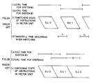
- FIGS.2A and 2B illustrate the relations between the switching between the scalar units 12 and 13 and respective CPU operating times.
- the CPU timer of the scalar unit 12 (system #0) records the CPU operating time during the time when the vector unit 14 is coupled to the scalar unit 12.
- the scalar unit 13 (system #1) becomes coupled to the vector unit 14 in place of the scalar unit 12.
- the CPU timer of the scalar unit 12 stops recording the CPU operating time, and on the other hand, the CPU timer of the scalar unit 13 starts recording. In this case, it is possible to obtain an accurate CPU operating time; however an overhead occurring at the time of switching is large, and therefore, the above process is wasteful of time intervals t1 and t2.
- the scalar units 12 and 13 are selectively connected to the vector unit 14, before the vector unit 14 has processed all the vector instructions (in the illustrated case, the vector unit starts processing the vector instructions supplied from the scalar unit 13 when the execution of the last vector instruction related to the scalar unit 12 is started).
- the overhead time can extremely be reduced.
- the present invention makes it possible to selectively provide a timing with which the scalar unit to be connected to the vector unit 14 is switched.
- the vector control unit 16 includes fetch stages 4 and 5 (related to the scalar units 12 and 13, respectively), a switching circuit 6, three stages 7, 8 and 9 provided for the pipeline processing of vector instructions, a switching control circuit 10, and a mode setting switch 11.
- the mode setting switch 11 is used for selecting one of a plurality of switching modes (three modes A, B and C are provided in the illustrated structure).
- the switching control circuit 10 is informed of the selected mode by a switching mode signal supplied from the mode setting switch 11.
- the switching control circuit 10 is supplied with state indicating signals a through e, which are output from the fetch stages 4, 5, and the first, second and third stages 7, 8, 9, respectively.
- state indicating signals a through e become indicative of the switching mode designated by the mode setting switch 11
- the switching control circuit 10 supplies a related switch signal to the switching circuit 6.
- each of the state indicating signals represents presence/absence of a vector instruction therein.
- each state indicating signal indicates the scalar unit to which the stored vector instruction is related.
- the mode setting switch selects one of the switching modes A, B and C.
- Examples of the switching modes A, B and C are as follows.
- the switching mode A is a mode in which the switching is performed when all vector instructions related to one of the scalar units 12 and 13 completely go out of all the stages 4, 5, 7, 8 and 9.
- the switching mode B is a mode in which the switching is performed when vector instructions related to one of the scalar units 12 and 13 completely go out of the third stage 9.
- the mode C is a mode in which the switching is performed when vector instructions related to one of the scalar units 12 and 13 completely go out of the second stage 8.
- the switching control circuit 10 outputs the switch signal when the selected state is detected.
- the right to use the vector unit 14 is given to the selected one of the scalar units 12 and 13.
- the CPU timer of the selected scalar unit is started, supplied from a timer control signal, which is derived from the switching circuit 6 and is supplied to the scalar units 12 and 13 through signal lines L1 and L2.
- the number of stages to be cascaded is not limited to 3.
- the mode A is selected by the mode setting switch 11.
- the mode B or C is selected by the mode setting switch 11.
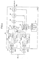
- FIG.4 there is illustrated a configuration of the structure of the vector control unit 16 constructed according to the embodiment of the present invention.
- the scalar units 12 and 13 are connected to vector fetch stages 23 and 24 (VFS0, VFS1) through buses BUS1 and BUS2, respectively.
- the vector fetch stage 23 includes a vector fetch stage register (VFSR0) 23-1, a vector fetch buffer (VFB0) 23-2, and a selector (SEL) 23-3.
- the vector fetch stage 23 includes a logic circuit, which will be described in detail later.
- the vector fetch stage (VFS1) 24 includes a vector fetch register (VFSR1) 24-1, a vector fetch buffer (VFB1) 24-2, a selector (SEL) 24-3, and a logic circuit (not shown).
- the vector fetch stages 23 and 24 correspond to the fetch stages 4 and 5 shown in FIG.3, respectively.
- the selectors 23-3 and 24-3 are connected to a switching circuit 25, which corresponds to the switching circuit 6 illustrated in FIG.3.
- the switching circuit 25 is followed by a vector pre-decode stage (VPS) 28, which indicates one of the scalar units 12 and 13 to which a vector instruction existing therein is related.
- the state indicating signal related to the vector pre-decode stage 28 is generated therein and supplied to a switching control circuit 26.
- the vector pre-decode stage 28 and the switching control circuit 26 correspond to the first stage 7 and the switching control circuit 10 shown in FIG.3, respectively.
- the switching control circuit 26 is supplied with busy signals derived from the aforementioned logic circuits provided in the vector fetch stages 23 and 24. The busy signals will be described in detail later.
- the vector pre-decode stage 28 proceeds to a vector queue stage (VQS) 29, which temporarily stores vector instructions supplied from the vector pre-decode stage 28.
- VQS vector queue stage
- the state indicating signal related to the vector queue stage 29 is generated therein and supplied to the switching control circuit 26.
- the vector queue stage 29 corresponds to the second stage 8 shown in FIG.3.
- a vector execute stage (VES) 30 follows the vector queue stage 30, and includes a supervisory register related to each of the pipelines 150, 151, 153, 154 and 155 shown in FIG.1.
- the supervisory registers store data which controls the start and end of the execution of the vector instructions to be executed in the corresponding pipelines 150, 151, 153, 154 and 155.
- the stage indicating signal related to the vector execute stage 30 is generated therein and supplied to the switching control circuit 26.
- the vector execute stage 30 corresponds to the third stage 9 shown in FIG.3.
- a mode setting circuit 27 is connected to the switching control circuit 26, and selects one of the three switching modes by closing the corresponding contact.
- the mode setting circuit 27 corresponds to the mode setting circuit 10 shown in FIG.3.
- vector instructions from the scalar units 12 and 13 are supplied to the vector fetch registers 23-1 and 24-1 through the buses BUS1 and BUS2, respectively.
- system #0 an operation related to the scalar unit 12
- the following operation is carried out.
- the fetched vector instruction is supplied from the vector fetch register 23-1 to the vector pre-decode stage 28 through the selector 23-3 and the switching circuit 25.
- the fetched vector instruction relating to the scalar unit 12 is transferred from the vector fetch register 23-1 to the vector fetch buffer 23-2, and is stored therein.
- a vector instruction which is placed at the top of the vector instructions stored in the vector fetch buffer 23-2, is read out of the vector fetch buffer 23-2, when the switching circuit 25 selects the scalar unit 12.
- the switching control circuit 26 selectively determines which one of the vector instructions sent from the scalar units 12 and 13 should be selected and supplied to the vector pre-decode stage 28.
- This switching control means the switching of the right to use the vector unit 14 in a unit of instruction packet.
- An instruction packet is defined as a sequence of consecutive vector instructions which can successively be executed with no interruption -thereof. Therefore, for example, the switching circuit 25 operates in such a manner that an instruction packet relating to the scalar unit 12 is completely executed, and thereafter the execution of an instruction packet relating to the scalar unit 13 is started.
- the right to use the vector unit 14 is exclusively switchable between the scalar units 12 and 13.
- vector instructions related to one of the scalar units 12 and 13 which has obtained the right are set the vector pre-decode stage 28 at the next operating stage.
- the vector instruction selected by the selector 25 in accordance with the switch signal supplied from the switching control circuit 26, is decoded by the vector pre-decode stage 28. Thereby, it can be found which one of the scalar units 12 and 13 the received vector instruction relates to. Then, the vector instruction in the vector pre-decode stage 28 is stored in the vector queue stage 29. Thereafter, the vector instruction read out of the vector queue stage 29 is supplied to the vector execute stage 30, which manages the access to the main memory unit la (FIG.1) and operation. At the same time as the vector execute stage 30 receives the vector instruction, it sends supervisory information to one of the pipelines 150, 151, 153, 154 and 155 to be executed. Thereafter, when the execution of the vector instruction is completed, the used pipeline is released from the execution.
- the switching control circuit 26 is supplied with the switching mode signal indicative of one of the switching modes M1, M2 and M3 selected by the mode setting switch 27.
- the switching control circuit 26 includes a first busy detecting circuit 26-1 shown in FIG.5A relating to the scalar unit 12 (system #0), and a second busy detecting circuit 26-2 shown in FIG.5B relating to the scalar unit 13 (system #1).
- An output signal of each of the first and second busy detecting circuits 26-1 and 26-2 is supplied to the switching circuit 25, a detailed configuration of which is illustrated in FIG.6.
- a busy signal VFS0-BUSY0 generated by the vector fetch register 23-1 is supplied to OR gates 31, 32 and 33.
- the busy signal VFS0-BUSY0 indicates whether or not a vector instruction relating to system #0 exists in the vector fetch stage 23.
- a busy signal VPS-BUSY0 generated by the vector pre-decode stage 28 is supplied to the OR gates 31, 32 and 33.
- the busy signal VPS-BUSY0 indicates whether or not a vector instruction relating to system #0 exists in the vector pre-decode stage 28.
- a busy signal VQS-BUSY0 generated by the vector queue stage 29 is supplied to the OR gates 31 and 32.
- the busy signal VQS-BUSY0 indicates whether or not a vector instruction relating to system #0 exists in the vector queue stage 29.
- a busy signal VES-BUSY0 generated by the vector execute stage 30 is supplied to the OR gate 31.
- the busy signal VES-BUSY0 indicates whether or not a vector instruction relating to system #0 exists in the vector execute stage 30.
- Output terminals of the OR gates 31, 32 and 33 are connected to input terminals of AND gates 34, 35 and 36, respectively.
- the switching mode signals M1, M2 and M3 derived from the mode setting circuit 27 are supplied to the AND gates 34, 35 and 36, respectively.
- Output terminals of the AND gates 34, 35 and 36 are connected to input terminals of an OR gate 37, which outputs a busy signal BUSY0.
- Each of the above-mentioned busy signals VFS0-BUSY0, VPS-BUSY0, VQS-BUSY0 and VES-BUSY0 is "1" when a vector instruction exists in the related stage, and is "0" when no vector instruction exists in the related stage.
- the OR gate 31 outputs "1” when a vector instruction exists in at least one of the four stages 23, 28, 29 and 30.
- the OR gate 32 outputs "1" when a vector instruction exists in at least one of the three stages 23, 28 and 29.
- the OR gate 33 outputs "1" when a vector instruction exists in at least one of the two stages 23 and 28.
- the AND gate 34 performs an AND operation on the output signal of the OR gate 31 and the switching mode signal M1.
- the AND gate 35 performs an AND operation on the output signal of the OR gate 32 and the switching mode signal M2.
- the AND gate 36 performs an AND operation on the output signal of the OR gate 33 and the switching mode signal M3.
- the aforementioned busy signal BUSY0 is generated by performing an OR operation on the output signals of the AND gates 34, 35 and 36 in the OR gate 37.
- the busy signal BUSY0 When the busy signal BUSY0 is "1", the busy signal BUSY0 represents that it is impossible to perform the switching based on the designated switching mode, or in other words, there are vector instructions relating to system #0 in the designated stages. On the other hand, when the busy signal BUSY0 is switched to "0", this change of the busy signal BUSY0 represents that all vector instructions relating to system #0 have gone out of the designated stages and therefore the switching from system #0 to system #1 becomes available.
- a busy signal VFS1-BUSY1 generated by the vector fetch register 23-1 is supplied to OR gates 41, 42 and 43.
- the busy signal VFS1-BUSY1 indicates whether or not a vector instruction relating to system #1 exists in the vector fetch stage 24.
- a busy signal VPS-BUSY1 generated by the vector pre-decode stage 28 is supplied to the OR gates 41, 42 and 43.
- the busy signal VPS-BUSY1 indicates whether or not a vector instruction relating to system #1 exists in the vector pre-decode stage 28.
- a busy signal VQS-BUSY1 generated by the vector queue stage 29 is supplied to the OR gates 41 and 42.
- the busy signal VQS-BUSY1 indicates whether or not a vector instruction relating to system #1 exists in the vector queue stage 29.
- a busy signal VES-BUSY1 generated by the vector execute stage 30 is supplied to the OR gate 41.
- the busy signal VES-BUSY1 indicates whether or not a vector instruction relating to system #1 exists in the vector execute stage 30.
- Output terminals of the OR gates 41, 42 and 43 are connected to input terminals of AND gates 44, 45 and 46, respectively.
- the switching mode signals M1, M2 and M3 derived from the mode setting circuit 27 are supplied to the AND gates 44, 45 and 46, respectively.
- Output terminals of the AND gates 44, 45 and 46 are connected to input terminals of an OR gate 47, which outputs a busy signal BUSY 1.
- Each of the above-mentioned busy signals VFS1-BUSY1, VPS-BUSY1, VQS-BUSY1 and VES-BUSY1 is "1" when a vector instruction exists in the related stage, and is "0" when no vector instruction exists in the related stage.
- the OR gate 41 outputs "1” when a vector instruction exists in at least one of the four stages 23, 28, 29 and 30.
- the OR gate 42 outputs "1" when a vector instruction exists in at' least one of the three stages 23, 28 and 29.
- the OR gate 43 outputs "1" when a vector instruction exists in at least one of the two stages 23 and 28.
- the AND gate 44 performs an AND operation on the output signal of the OR gate 41 and the switching mode signal M1.
- the AND gate 45 performs an AND operation on the output signal of the OR gate 42 and the switching mode signal M2.
- the AND gate 46 performs an AND operation on the output signal of the OR gate 43 and the switching mode signal M3.
- the aforementioned busy signal BUSY1 is generated by performing an OR operation on the output signals of the AND gates 44, 45 and 46 in the OR gate 47.
- the busy signal BUSY1 When the busy signal BUSY1 is "1", the busy signal BUSY1 represents that it is impossible to perform the switching based on the designated switching mode, or in other words, there are vector instructions relating to system #1 in the designated stages. On the other hand, when the busy signal BUSY1 is switched to "0", this change of the busy signal BUSY1 represents that all vector instructions relating to system #1 have gone out of the designated stages, and therefore the switching from system #1 to system #0 becomes available.
- FIG.6 illustrates an example of the structure for the switching circuit 25.
- the switching circuit 25 includes a set-reset type latch circuit (SR0) 50 in which a set operation has priority over a reset operation, a set-reset type latch circuit (SR1) 51 in which a reset operation has priority over a set operation, AND gates 52, 53, an OR gate 54, and inverters 55, 56, 57 and 58.
- SR0 set-reset type latch circuit
- SR1 set-reset type latch circuit
- the output signal of the latch circuit 50 passes through the inverter 57 and is then supplied to the scalar unit 12.
- the output signal of the inverter 57 is "1" when the scalar unit 12 is not selected. At this time, the CPU timer of the scalar unit 12 is stopped.
- the output signal of the latch circuit 51 passes through an inverter 58 and is then supplied to the scalar unit 13.
- the output signal of the inverter 58 is "1" when the scalar unit 13 is not selected. At this time, the CPU timer of the scalar unit 13 is stopped.
- Operation occurring at the time of switching from system #1 to system #0 is similar to that for the switching from system #0 to system #1.
- the vector fetch stage 23 includes a logic circuit 23-4 in addition to the aforementioned vector fetch register (VFSR0) 23-1, vector fetch buffer (VFB0) 23-2, and selector (SEL) 23-3.
- the vector fetch register 23-1 includes a flag register VFSR0-VALID.
- the vector fetch buffer 23-2 includes buffer portions VFB00 and VFB01. When a vector instruction is being registered in the buffer portion VFB00, "1" is set in an associated flag register VFB00-VALID. For the same purpose, a flag register VFB01-VALID is provided with respect to the buffer portion VFB01.
- the selector 23-3 includes AND gates 23a, 23b, and an OR gate 23c.
- the AND gates 23a and 23b are connected to the vector fetch register 23-1 and the vector fetch buffer 23-2, respectively. Further, the AND gates 23a and 23b are supplied with select signals SELECT-VFSR0 and SELECT-VFB0, respectively, which are generated by the logic circuit 23-4. Output terminals of the AND gates 23a and 23b are connected to the OR gate 23c, which is connected to the switching circuit 25.
- the logic circuit 23-4 is made up of OR gates 23d, 23e, and an inverter 23f.
- the OR gate 23d is supplied with the state signals stored in the flag registers VFB00-VALID and VFB01-VALID.
- the OR gate 23e is supplied with the state signal stored in the flag register VFSR0-VALID and an output signal of the OR gate 23d.
- the output signal of the OR gate 23d is the select signal SELECT-VFB0 to be supplied to the AND gate 23b, and is also supplied to the AND gate 23a through the inverter 23f, as the select signal SELECT-VFSR0.
- the output signal of the OR gate 23e is the aforementioned busy signal VFS0-BUSY0.
- a vector instruction supplied from the scalar unit 12 is set in the vector fetch register 23-1.
- a valid signal of "1" is set in the flag register VFSR0-VALID associated with the vector fetch register 23-1.
- the select signal SELECT VFSR0 is "1".
- the selector 23-3 selects the vector instruction supplied from the vector fetch register 23-1.
- FIG.9 illustrates an example of the structure for the vector pre-decode stage (VPS) 28.
- the vector pre-decode stage 28 includes a vector pre-decode stage register (VPSR) 28-1, and a logic circuit 28-2 made up of an inverter 28a and AND gates 28b and 28c.
- the vector pre-decode stage register 28-1 includes flag registers VPSR-SU1 and VPSR-VALID.
- VPSR-SU1 flag registers VPSR-SU1
- VPSR-VALID When a vector instruction is supplied to the vector pre-decode stage register 28-1 from the vector fetch stage 23, a value of "1" is written into the flag register VPSR-VALID, and a value of "0" is written into the register VPSR-SU1.
- the state where there are values of "1" and "0" in the flag registers VPSR-VALID and VPSR-SU1, respectively, means that a vector instruction relating to system #0 is set in the vector pre-decode flag register 28-1.
- the logic circuit 28-2 sets the busy signal VPS-BUSY0 to "1".
- the valid signal stored in the flag register VPSR-VALID is supplied to the AND gates 28b and 28c.
- the state signal stored in the flag register VPSR-SU1 is supplied to the AND gate 28b, and the AND gate 28c through the inverter 28a.
- the AND gates 28b and 28c output the busy signals VPS-BUSY0 and VPS-BUSY1, respectively.
- the state where a value of "1" is set in each of the flag registers VPSR-VALID and VPSR-SU1, means that a vector instruction relating to system #1 is set in the vector pre-decode stage register 28-1.
- the busy signal VPS-BUSY1 is set to "1".
- the busy signals VPS-BUSY0 and VPS-BUSY1 are sent to the switching control circuit 26.
- FIG.10 illustrates an example of the structure for the vector queue stage 29.
- the vector queue stage 29 includes a register (AQSR) 29-1, a register (EQSR) 29-2, a selector (SEL) 29-3, and a logic circuit 29-4.
- the register 29-1 includes flag registers AQS-VALID and AQS-SU1
- the register 29-2 includes flag registers EQS-VALID and EQS-SU1.
- the register 29-2 includes flag registers EQS-VALID and EQS-SU1.
- the vector instruction is a vector instruction which uses one of the addition pipeline 153, the multiplication pipeline 154 and the division pipeline 155
- the above vector instruction is written into the register 29-2.
- the valid signal stored in the flag register VPSR-VALID shown in FIG.9 is set in either the flag register AQS-VALID or EQS-VALID.
- the state signal stored in the flag register VPSR-SU1 is set in either the flag register AQS-SU1 or the register EQS-SU1.
- the vector instructions in the registers 29-1 and 29-2 are sequentially read out starting from an executable vector instruction contained therein, and are supplied to the vector execute stage 30.
- the valid signal stored in the flag register AQSR-VALID is supplied to AND gates 29a and 29b of the logic circuit 29-4.
- the state signal stored in the flag register AQS-SU1 is supplied to the AND gate 29b, and the AND gate 29a through an inverter 29e.
- the output signals of the AND gates 29a and 29b are supplied to OR gates 29g and 29h, respectively.
- the valid signal stored in the flag register EQS-VALID is supplied to the AND gates 29c and 29d.
- the state signal stored in the flag register EQS-SU1 is supplied to the AND gate 29d, and the AND gate through an inverter 29f.
- the output signals of the AND gates 29c and 29d are supplied to the OR gates 29g and 29h, respectively.
- the OR gates 29g and 29h output the busy signals VQS-BUSY0 and VQS-BUSY1, respectively, which are supplied to the switching control circuit 26.
- the busy signal VQS-BUSY0 is "1"
- the value of the busy signal VQS-BUSY1 is determined.
- the busy signals VQS-BUSY0 and VQS-BUSY1 generated in this manner are supplied to the switching control circuit 26.
- the vector execute stage 30 has the illustrated supervisory circuit for each of the load pipeline 150, the store pipeline 151, the addition pipeline 153, the multiplication pipeline 154 and the division pipeline 155.
- the following description relates to the structure of the supervisory circuit provided for the load pipeline 150 (a load supervisory circuit).
- the supervisory circuit is made up of a register (LRSR) 30-1, a register (LWSR) 30-2, counters 30-3, 30-4, and a logic circuit 30-5.
- LRSR register
- LWSR register
- a vector instruction supplied from the vector queue stage 29 is set in the register 30-1, which includes flag registers LRSR-VALID and LRSR-SU1.
- the counter 30-3 is set to 0, and starts counting.
- the vector instruction stored in the register 30-1 is supplied to the load pipeline 150 through the signal line 160.
- the counter 30-3 counts a value determined by the received vector instruction (read time)
- the vector instruction is read out of the register 30-1 and is then set in the register 30-2.
- the counter 30-4 is set to "0", and then starts counting.
- the counted value of the counter 30-4 reaches a value indicative of a time it takes to execute the vector instruction of concern (write time)
- the execution of the vector instruction is ended.
- the above circuit is the same as the logic circuit 29-4 shown in FIG.10.
- the busy signal LSR-BUSY0 is "1".
- the busy signal LSR-BUSY1 is "1".
- An OR gate 30i included in the logic circuit 30-5 is supplied to busy signals LSR-BUSY0, SSR-BUSY0, ASR-BUSY0, MSR-BUSY0, and DSR-BUSY0 with respect to the pipelines 150, 151, 153, 154 and 155, respectively. Then the OR gate generates a busy signal VES-BUSY0, which is supplied to the switching control circuit 26. Similarly, an OR gates 30j generates a busy signal VES-BUSY1 from busy signals LSR-BUSY1, SSR-BUSY1, ASR-BUSY1, MSR-BUSY1, and DSR-BUSY1 with respect to the pipelines 150, 151, 153, 154 and 155, respectively. The busy signals VES-BUSY0 and VES-BUSY1 thus generated are supplied to the switching control circuit 26.
- the present invention is not limited to the above-mentioned embodiment.
- an arbitrary number of stages provided in the vector control unit 16 may be used.
- the busy signal generated at each stage may be generated based only on whether one of the scalar units 12 and 13 is related to the stored vector instruction. This is because the scalar units 12 and 13 are alternately selected.
- the above-mentioned embodiment relates to a multiprocessor system having a plurality of scalar units and a single vector unit.
- the present invention includes a multiprocessor system which includes a plurality of small-scale execution units and a single large-scale execution unit.
Landscapes
- Engineering & Computer Science (AREA)
- Theoretical Computer Science (AREA)
- Software Systems (AREA)
- Physics & Mathematics (AREA)
- General Engineering & Computer Science (AREA)
- General Physics & Mathematics (AREA)
- Computer Hardware Design (AREA)
- Multimedia (AREA)
- Computing Systems (AREA)
- Advance Control (AREA)
- Complex Calculations (AREA)
- Multi Processors (AREA)
Claims (21)
- Système de commande de multiprocesseur adapté à un système de multiprocesseur incluant une pluralité de premières unités d'exécution (12, 13) dont chacune traite un premier groupe d'instructions et une unique seconde unité d'exécution (14) qui traite un second groupe d'instructions appliqué depuis ladite pluralité de premières unités d'exécution, ladite seconde unité d'exécution incluant une pluralité de pipelines (150, 151, 153 - 155) utilisés pour exécuter ledit second groupe d'instructions, ledit système de commande de multiprocesseur comprenant en outre un moyen de commutation (6 ; 25) sensible à un signal de commutation pour commuter sélectivement ledit second groupe d'instructions appliqué depuis lesdites premières unités d'exécution pour ainsi sélectionner ledit second groupe d'instructions en relation avec l'une de ladite pluralité de premières unités d'exécution ; et
un moyen d'étage de commande (4, 5, 7 - 9 ; 23, 24, 28 - 30) incluant une pluralité d'étages de registre utilisés pour commander un processus en pipeline pour stocker séquentiellement ledit second groupe d'instructions concernant ladite une sélectionnée desdites premières unités d'exécution dans lesdits étages de registre, caractérisé en ce que ledit moyen d'étage de commande est agencé pour émettre en sortie, pour chaque étage de registre, un signal d'indication d'état indiquant une information d'état concernant l'étage de registre correspondant ; et en ce que ledit système de commande de multiprocesseur comprend en outre :
un moyen d'établissement de mode de commutation (11, 27) pour générer un signal d'établissement de mode utilisé pour sélectionner l'un d'une pluralité de modes de commutation (M1, M2, M3) dont chacun définit un cadencement selon lequel la commutation par ledit moyen de commutation est effectuée ; et
un moyen de commande de commutation (10 ; 26) pour générer ledit signal de commutation sur la base desdits signaux d'indication d'état émis en sortie depuis ledit moyen d'étage de commande et dudit signal d'établissement de mode indicatif de l'un de la pluralité de modes de commutation appliqué depuis ledit moyen d'établissement de mode de commutation. - Système de commande de multiprocesseur selon la revendication 1, caractérisé en ce que ladite pluralité d'étages de registre (4, 5, 7 - 9 ; 23, 24, 28 - 30) inclus dans ledit moyen d'étage de commande sont mis en cascade et en ce que ladite pluralité de modes de commutation (M1, M2, M3) inclut un premier mode de commutation (M1) dans lequel la commutation par ledit moyen de commutation (6 ; 25) est effectuée lorsque toutes les instructions concernant ledit second groupe appliquées depuis l'une de ladite pluralité de premières unités d'exécution sortent complètement de tous les étages de registre.
- Système de commande de multiprocesseur selon l'une quelconque des revendications 1 ou 2, caractérisé en ce que ladite pluralité d'étages de registres (4, 5, 7 - 9 ; 23, 24, 28 - 30) inclus dans ledit moyen d'étage de commande sont mis en cascade et ladite pluralité de modes de commutation (M1, M2, M3) incluent un second mode de commutation (M2) dans lequel la commutation par ledit moyen de commutation (6 ; 25) est effectuée lorsque toutes les instructions concernant ledit second groupe appliquées depuis l'une de ladite pluralité de premières unités d'exécution sortent complètement de tous lesdits étages de registre mis en cascade sauf du dernier (9, 30) qui est situé au niveau de l'extrémité de ceux-ci, et ledit second groupe d'instructions stockées dans ledit moyen d'étage de commande est appliqué sur l'un desdits pipelines par l'intermédiaire dudit dernier étage de registre (9, 30) situé au niveau de l'extrémité desdits étages de registre mis en cascade.
- Système de commande de multiprocesseur selon l'une quelconque des revendications 1 à 3, caractérisé en ce que ladite pluralité d'étages de registre (4, 5, 7 - 9 ; 23, 24, 28 - 30) inclus dans ledit moyen d'étage de commande sont mis en cascade et ladite pluralité de modes de commutation (M1, M2, M3) incluent un troisième mode de commutation (M3) dans lequel la commutation par ledit moyen de commutation (6 ; 25) est effectuée lorsque toutes les instructions concernant ledit second groupe appliquées depuis l'une de ladite pluralité de premières unités d'exécution sortent complètement de tous lesdits étages de registre mis en cascade sauf des deux derniers (8, 9 ; 29 ; 30), et ledit second groupe d'instructions stockées dans ledit moyen d'étage de commande sont appliquées sur lesdits pipelines par l'intermédiaire dudit dernier étage de registre (9, 30) situé au niveau de l'extrémité desdits étages mis en cascade.
- Système de commande de multiprocesseur selon l'une quelconque des revendications 1 à 4, caractérisé en ce qu'il comprend en outre un moyen (6, 25, L1, L2) pour appliquer un signal indicatif dudit cadencement de commutation à chacune de ladite pluralité de premières unités d'exécution (12, 13).
- Système de commande de multiprocesseur selon la revendication 5, caractérisé en ce que chacune desdites premières unités d'exécution (12, 13) comprend une minuterie utilisée pour enregistrer un temps de fonctionnement sur la base dudit signal indicatif dudit cadencement de la commutation.
- Système de commande de multiprocesseur selon l'une quelconque des revendications 1 à 6, caractérisé en ce que ledit moyen d'étage de commande comprend, pour chaque étage de registre, un moyen de génération (23-4, 28-2, 29-4, 30-5) pour générer ledit signal d'indication d'état pour chacune de ladite pluralité de premières unités d'exécution (12, 13) et en ce que ledit signal d'indication d'état généré pour chacune desdites premières unités d'exécution indique si oui ou non au moins l'une dudit second groupe d'instructions est stockée dans l'étage de registre correspondant.
- Système de commande de multiprocesseur selon l'une quelconque des revendications 1 à 7, caractérisé en ce que ledit système de multiprocesseur comprend deux premières unités d'exécution (12, 13) ;
ledit moyen de commande de commutation (26) comprend un premier moyen de détection d'état occupé (26 - 1) concernant l'une (12) desdites deux premières unités d'exécution, pour déterminer si oui ou non le mode de commutation établi par ledit moyen d'établissement de mode de commutation (27) peut être réalisé en se référant audit signal d'indication d'état appliqué depuis chacun desdits étages de registre (4, 5, 7 - 9 ; 23, 24, 28 - 30) et audit signal d'établissement de mode de commutation appliqué depuis ledit moyen d'établissement de mode de commutation (27) et pour générer un premier signal d'état occupé (BUSY0) indicatif du résultat de la détermination, et un second moyen de détection d'état occupé (26 - 2) concernant l'autre (13) desdites deux premières unités d'exécution, pour déterminer si oui ou non le mode commutation établi par ledit moyen d'établissement de mode de commutation (27) peut être réalisé en se référant audit signal d'indication d'état appliqué depuis chacun desdits étages de registre et audit signal d'établissement de mode appliqué depuis ledit moyen d'établissement de mode de commutation et pour générer un second signal d'état occupé (BUSY1) indicatif du résultat de la détermination ; et
lesdits premier et second signaux d'états occupés sont appliqués en tant que dit signal de commutation audit moyen de commutation. - Système de commande de multiprocesseur selon la revendication 8, caractérisé en ce que chacun desdits premier et second moyens de détection d'état occupé (26 - 1, 26 - 2) comprend :
une pluralité de portes OU (31 - 33 ; 41 - 43) dont chacune réalise une opération OU sur lesdits signaux d'indication d'état appliqués depuis deux étages de registre ou plus parmi ladite pluralité d'étages de registre pour ainsi émettre en sortie un résultat d'opération OU ;
une pluralité de portes ET (34 - 36 ; 44 - 46) respectivement prévues pour lesdites portes OU, chacune réalisant une opération ET sur ledit résultat d'opération OU appliqué depuis l'une considérée desdites portes OU et depuis l'un de ladite pluralité de modes de commutation (M1, M2, M3) pour ainsi émettre en sortie un résultat d'opération ET ; et
une porte OU (37 ; 47) qui réalise une opération OU sur lesdits résultats d'opération ET appliqués depuis ladite pluralité de portes ET pour ainsi émettre en sortie ledit premier ou second signal d'état occupé (BUSY0, BUSY1) qui doit être appliqué audit circuit de commutation. - Système de commande de multiprocesseur selon l'une quelconque des revendications 1 à 9, caractérisé en ce que :
ledit système de multiprocesseur comprend deux premières unités d'exécution (12, 13) ; et
ledit moyen d'étage de commande comprend un premier moyen de registre de recherche (23) connecté entre l'une (12) desdites premières unités d'exécution et ledit moyen de commutation (25), pour rechercher ledit second groupe d'instructions dans ladite une considérée desdites premières unités d'exécution ; et
un second moyen de registre de recherche (24) connecté entre l'autre (13) desdites premières unités d'exécution et ledit moyen de commutation (25) pour rechercher ledit second groupe d'instructions dans l'autre desdits premiers moyens d'exécution. - Système de commande de multiprocesseur selon la revendication 10 lorsqu'elle dépend de la revendication 8, caractérisé en ce ledit moyen de commutation (25) comprend :
des première et seconde bascules (50, 51) dont chacune comprend des bornes d'établissement et de remise à l'état initial, des premier et second inverseurs (55, 56), des première et seconde portes ET (52, 53) et une porte OU (54) ;
ledit premier signal d'état occupé (BUSY0) est appliqué par l'intermédiaire dudit premier inverseur sur la borne de remise à l'état initial de ladite première bascule et sur la borne d'établissement de ladite seconde bascule ;
ledit second signal d'état occupé (BUSY1) est appliqué par l'intermédiaire dudit second inverseur sur ladite borne d'établissement de ladite première bascule et sur la borne de remise à l'état initial de ladite seconde bascule ;
des sorties desdites première et seconde bascules (50, 51) sont respectivement appliquées sur lesdites première et seconde portes ET (52, 53) et lesdites première et seconde portes ET se voient appliquer ledit second groupe d'instructions concernant respectivement lesdites premières unités d'exécution ainsi que lesdits seconds moyens de registre de recherche (23, 24) ; et
des sorties desdites première et seconde portes ET sont appliquées sur ladite porte OU (54), laquelle émet en sortie ledit second groupe d'instructions concernant ladite sélectionnée des premières unités d'exécution sur ledit moyen d'étage de commande. - Système de commande de multiprocesseur selon la revendication 11, caractérisé en ce que la borne d'établissement de ladite première bascule (50) a priorité sur sa borne de remise à l'état initial et la borne de remise à l'état initial de ladite seconde bascule (51) a priorité sur sa borne d'établissement.
- Système de commande de multiprocesseur selon la revendication 12, caractérisé en ce que ledit moyen de commutation (25) comprend en outre des troisième et quatrième inverseurs (57, 58) utilisés pour inverser les sorties respectives desdites première et seconde bascules (50, 51) et des sorties inversées sont des signaux utilisés pour commander les minuteries desdites premières unités d'exécution concernées (12, 13).
- Système de commande de multiprocesseur selon l'une quelconque des revendications 10 à 13, caractérisé en ce que chacun des premier et second moyens de registre de recherche (23 ; 24) comprend un registre (23 - 1) qui stocke temporairement le second groupe d'instructions appliquées depuis la première unité d'exécution correspondante (12), un tampon (23 - 2) qui tamponne le second groupe d'instructions appliquées depuis la première unité d'exécution correspondante, un sélecteur (23 - 3) qui sélectionne l'un desdits registre et tampon pour connecter celui sélectionné desdits registre et tampon audit moyen de commutation et un moyen logique (23 - 4) pour générer ledit signal d'indication d'état (VFS0 - BUSY0 ; VFS1 - BUSY1) sur la base des contenus de stockage desdits registre et tampon.
- Système de commande de multiprocesseur selon l'une quelconque des revendications 1 à 14, caractérisé en ce que ledit moyen d'étage de commande comprend un moyen de registre de prédécodage (28 - 1) connecté audit moyen de commutation (25) pour décoder ledit second groupe d'instructions appliquées depuis l'une sélectionnée desdites premières unités d'exécution par l'intermédiaire dudit moyen de commutation pour déterminer laquelle desdites premières unités d'exécution est associée audit second groupe d'instruction appliquées et un moyen logique (28 - 2) pour générer ledit signal d'indication d'état (VPS - BUSY0 ; VPS - BUSY1) sur la base des contenus de stockage dudit moyen de registre de prédécodage.
- Système de commande de multiprocesseur selon la revendication 15, caractérisé en ce que ledit moyen d'étage de commande comprend un premier moyen de registre de file d'attente (29 - 1) connecté audit moyen de prédécodage (28) pour mettre en file d'attente ledit second groupe d'instructions concernant certains (150, 151) desdits pipelines et appliquées depuis ledit moyen de registre de prédécodage, un second moyen de registre de file d'attente (29 - 2) connecté audit moyen de prédécodage pour mettre en file d'attente ledit second groupe d'instructions concernant le reste (153 - 155) desdits pipelines et appliqué depuis ledit moyen de registre de prédécodage, un sélecteur (29 -3) pour sélectionner l'un desdits premier et second moyens de registre de file d'attente de telle sorte que le second groupe d'instructions concernant le moyen sélectionné pris parmi lesdits premier et second moyens de registre de file d'attente, et un moyen logique (29 - 4) pour générer ledit signal d'indication d'état (VQS - BUSY0, VQS - BUSY1) sur la base des contenus de stockage desdits premier et second moyens de registre de file d'attente.
- Système de commande de multiprocesseur selon la revendication 16, caractérisé en ce que ledit moyen d'étage de commande comprend un moyen de surveillance (30-1, 30-2, 30-3, 30-4) pour stocker ledit second groupe d'instructions qui doivent être appliquées sur l'un desdits pipelines et un moyen logique (30-5) pour générer ledit signal d'indication d'état (LSR - BUSY0, LSR - BUSY1) sur la base des contenus de stockage dudit moyen de registre de surveillance.
- Système de commande de multiprocesseur selon la revendication 17, caractérisé en ce que ledit moyen de surveillance (30-1, 30-2, 30-3, 30-4) stocke ledit second groupe d'instructions pour chaque pipeline.
- Système de commande de multiprocesseur selon l'une quelconque des revendications 1 à 18, caractérisé en ce que ledit moyen de commutation (6, 25), ledit moyen d'étage de commande (4, 5, 7 - 9 ; 23, 24, 28 - 30), ledit moyen d'établissement de mode de commutation, (11, 27) et ledit moyen de commande de commutation (10, 26) sont prévus dans ladite seconde unité d'exécution.
- Système de commande de multiprocesseur selon l'une quelconque des revendications 1 à 19, caractérisé en ce que chacune desdites premières unités d'exécution (12, 13) est une unité scalaire et ladite seconde unité d'exécution est une unité vectorielle.
- Système de commande de multiprocesseur selon l'une quelconque des revendications 1 à 19, caractérisé en ce que chacune desdites premières unités d'exécution (12, 13) est une unité d'exécution petite échelle et ladite seconde unité d'exécution est une unité d'exécution grande échelle.
Applications Claiming Priority (2)
| Application Number | Priority Date | Filing Date | Title |
|---|---|---|---|
| JP140297/88 | 1988-06-07 | ||
| JP63140297A JPH06105460B2 (ja) | 1988-06-07 | 1988-06-07 | マルチプロセッサのプロセッサ切換え装置 |
Publications (3)
| Publication Number | Publication Date |
|---|---|
| EP0346003A2 EP0346003A2 (fr) | 1989-12-13 |
| EP0346003A3 EP0346003A3 (fr) | 1991-06-05 |
| EP0346003B1 true EP0346003B1 (fr) | 1994-08-24 |
Family
ID=15265510
Family Applications (1)
| Application Number | Title | Priority Date | Filing Date |
|---|---|---|---|
| EP89305523A Expired - Lifetime EP0346003B1 (fr) | 1988-06-07 | 1989-06-01 | Système de commande de multiprocesseur |
Country Status (5)
| Country | Link |
|---|---|
| US (1) | US5001627A (fr) |
| EP (1) | EP0346003B1 (fr) |
| JP (1) | JPH06105460B2 (fr) |
| CA (1) | CA1315006C (fr) |
| DE (1) | DE68917647T2 (fr) |
Families Citing this family (19)
| Publication number | Priority date | Publication date | Assignee | Title |
|---|---|---|---|---|
| JPH03233630A (ja) * | 1990-02-08 | 1991-10-17 | Nec Corp | 情報処理装置 |
| US5261063A (en) * | 1990-12-07 | 1993-11-09 | Ibm Corp. | Pipeline apparatus having pipeline mode eecuting instructions from plural programs and parallel mode executing instructions from one of the plural programs |
| RU1804645C (ru) * | 1991-03-27 | 1993-03-23 | Институт Точной Механики И Вычислительной Техники Им.С.А.Лебедева | Центральный процессор |
| US5530881A (en) * | 1991-06-06 | 1996-06-25 | Hitachi, Ltd. | Vector processing apparatus for processing different instruction set architectures corresponding to mingled-type programs and separate-type programs |
| IT1264302B1 (it) * | 1993-12-24 | 1996-09-23 | Rainer Srl | Macchina per la lavorazione di una lamiera. |
| US5663961A (en) * | 1995-02-24 | 1997-09-02 | Motorola, Inc. | Packet switch with centralized buffering for many output channels |
| US6535905B1 (en) | 1999-04-29 | 2003-03-18 | Intel Corporation | Method and apparatus for thread switching within a multithreaded processor |
| US6507862B1 (en) | 1999-05-11 | 2003-01-14 | Sun Microsystems, Inc. | Switching method in a multi-threaded processor |
| US6341347B1 (en) | 1999-05-11 | 2002-01-22 | Sun Microsystems, Inc. | Thread switch logic in a multiple-thread processor |
| US6542921B1 (en) | 1999-07-08 | 2003-04-01 | Intel Corporation | Method and apparatus for controlling the processing priority between multiple threads in a multithreaded processor |
| US6496925B1 (en) | 1999-12-09 | 2002-12-17 | Intel Corporation | Method and apparatus for processing an event occurrence within a multithreaded processor |
| US6889319B1 (en) | 1999-12-09 | 2005-05-03 | Intel Corporation | Method and apparatus for entering and exiting multiple threads within a multithreaded processor |
| US6357016B1 (en) | 1999-12-09 | 2002-03-12 | Intel Corporation | Method and apparatus for disabling a clock signal within a multithreaded processor |
| US7051329B1 (en) | 1999-12-28 | 2006-05-23 | Intel Corporation | Method and apparatus for managing resources in a multithreaded processor |
| US7856633B1 (en) | 2000-03-24 | 2010-12-21 | Intel Corporation | LRU cache replacement for a partitioned set associative cache |
| US7363474B2 (en) | 2001-12-31 | 2008-04-22 | Intel Corporation | Method and apparatus for suspending execution of a thread until a specified memory access occurs |
| US7127561B2 (en) | 2001-12-31 | 2006-10-24 | Intel Corporation | Coherency techniques for suspending execution of a thread until a specified memory access occurs |
| US8024735B2 (en) | 2002-06-14 | 2011-09-20 | Intel Corporation | Method and apparatus for ensuring fairness and forward progress when executing multiple threads of execution |
| US20250130799A1 (en) * | 2023-10-19 | 2025-04-24 | Ampere Computing Llc | Techniques for performing non-vector micro-operations on vector hardware |
Family Cites Families (7)
| Publication number | Priority date | Publication date | Assignee | Title |
|---|---|---|---|---|
| JPS5194734A (en) * | 1975-02-19 | 1976-08-19 | Tajushorisochino enzanseigyohoshiki | |
| JPS57155666A (en) * | 1981-03-20 | 1982-09-25 | Fujitsu Ltd | Instruction controlling system of vector processor |
| EP0105125B1 (fr) * | 1982-09-03 | 1989-04-19 | Hitachi, Ltd. | Système processeur de données |
| KR900001999B1 (ko) * | 1984-11-30 | 1990-03-31 | 후지쓰 가부시끼가이샤 | 멀티프로세서 시스템(multiprocessor system) |
| US4875161A (en) * | 1985-07-31 | 1989-10-17 | Unisys Corporation | Scientific processor vector file organization |
| US4903196A (en) * | 1986-05-02 | 1990-02-20 | International Business Machines Corporation | Method and apparatus for guaranteeing the logical integrity of data in the general purpose registers of a complex multi-execution unit uniprocessor |
| US4760525A (en) * | 1986-06-10 | 1988-07-26 | The United States Of America As Represented By The Secretary Of The Air Force | Complex arithmetic vector processor for performing control function, scalar operation, and set-up of vector signal processing instruction |
-
1988
- 1988-06-07 JP JP63140297A patent/JPH06105460B2/ja not_active Expired - Fee Related
-
1989
- 1989-06-01 DE DE68917647T patent/DE68917647T2/de not_active Expired - Fee Related
- 1989-06-01 EP EP89305523A patent/EP0346003B1/fr not_active Expired - Lifetime
- 1989-06-06 CA CA000601891A patent/CA1315006C/fr not_active Expired - Fee Related
- 1989-06-07 US US07/362,601 patent/US5001627A/en not_active Expired - Lifetime
Also Published As
| Publication number | Publication date |
|---|---|
| JPH06105460B2 (ja) | 1994-12-21 |
| EP0346003A3 (fr) | 1991-06-05 |
| DE68917647T2 (de) | 1994-12-22 |
| DE68917647D1 (de) | 1994-09-29 |
| JPH01309178A (ja) | 1989-12-13 |
| EP0346003A2 (fr) | 1989-12-13 |
| US5001627A (en) | 1991-03-19 |
| CA1315006C (fr) | 1993-03-23 |
Similar Documents
| Publication | Publication Date | Title |
|---|---|---|
| EP0346003B1 (fr) | Système de commande de multiprocesseur | |
| US4398244A (en) | Interruptible microprogram sequencing unit and microprogrammed apparatus utilizing same | |
| US4984151A (en) | Flexible, next-address generation microprogram sequencer | |
| US4685076A (en) | Vector processor for processing one vector instruction with a plurality of vector processing units | |
| EP0268264B1 (fr) | Système de commande pour processeur vectoriel | |
| US5148544A (en) | Apparatus and method for control of asynchronous program interrupt events in a data processing system | |
| EP0087978A2 (fr) | Unité de traitement d'informations | |
| EP0172038B1 (fr) | Processeur d'informations | |
| US4308581A (en) | Single step system for a microcomputer | |
| JPS6161436B2 (fr) | ||
| US5497496A (en) | Superscalar processor controlling fetching of instructions based upon number of empty instructions registers detected for each cycle | |
| EP0126247B1 (fr) | Système ordinateur | |
| JPH0332818B2 (fr) | ||
| US4777592A (en) | Information processing system comprising a register renewal waiting control circuit with renewal register number registering means | |
| EP0167959B1 (fr) | Traitement pour registres de vecteur de calculateur | |
| EP0223150B1 (fr) | Dispositif de traitement d'information | |
| US4837688A (en) | Multi-channel shared resource processor | |
| US5539902A (en) | Vector data processing apparatus wherein a time slot for access to a bank of vector registors is assigned based on memory access time information | |
| EP0240606B1 (fr) | Système de traitement en pipeline et microprocesseur utilisant le système | |
| EP0437207A2 (fr) | Système de traitement d'information | |
| AU626067B2 (en) | Apparatus and method for control of asynchronous program interrupt events in a data processing system | |
| KR900005284B1 (ko) | 마이크로 컴퓨터 | |
| US5050076A (en) | Prefetching queue control system | |
| US5355463A (en) | Circuit configuration for transforming the logical address space of a processor unit to the physical address space of a memory | |
| EP0416345B1 (fr) | Décodeur d'instructions pour un processeur pipeline |
Legal Events
| Date | Code | Title | Description |
|---|---|---|---|
| PUAI | Public reference made under article 153(3) epc to a published international application that has entered the european phase |
Free format text: ORIGINAL CODE: 0009012 |
|
| AK | Designated contracting states |
Kind code of ref document: A2 Designated state(s): DE FR GB |
|
| PUAL | Search report despatched |
Free format text: ORIGINAL CODE: 0009013 |
|
| AK | Designated contracting states |
Kind code of ref document: A3 Designated state(s): DE FR GB |
|
| 17P | Request for examination filed |
Effective date: 19910731 |
|
| 17Q | First examination report despatched |
Effective date: 19930311 |
|
| GRAA | (expected) grant |
Free format text: ORIGINAL CODE: 0009210 |
|
| AK | Designated contracting states |
Kind code of ref document: B1 Designated state(s): DE FR GB |
|
| REF | Corresponds to: |
Ref document number: 68917647 Country of ref document: DE Date of ref document: 19940929 |
|
| ET | Fr: translation filed | ||
| PLBE | No opposition filed within time limit |
Free format text: ORIGINAL CODE: 0009261 |
|
| STAA | Information on the status of an ep patent application or granted ep patent |
Free format text: STATUS: NO OPPOSITION FILED WITHIN TIME LIMIT |
|
| 26N | No opposition filed | ||
| REG | Reference to a national code |
Ref country code: GB Ref legal event code: IF02 |
|
| PGFP | Annual fee paid to national office [announced via postgrant information from national office to epo] |
Ref country code: DE Payment date: 20060525 Year of fee payment: 18 |
|
| PGFP | Annual fee paid to national office [announced via postgrant information from national office to epo] |
Ref country code: GB Payment date: 20060531 Year of fee payment: 18 |
|
| PGFP | Annual fee paid to national office [announced via postgrant information from national office to epo] |
Ref country code: FR Payment date: 20060608 Year of fee payment: 18 |
|
| GBPC | Gb: european patent ceased through non-payment of renewal fee |
Effective date: 20070601 |
|
| REG | Reference to a national code |
Ref country code: FR Ref legal event code: ST Effective date: 20080229 |
|
| PG25 | Lapsed in a contracting state [announced via postgrant information from national office to epo] |
Ref country code: DE Free format text: LAPSE BECAUSE OF NON-PAYMENT OF DUE FEES Effective date: 20080101 |
|
| PG25 | Lapsed in a contracting state [announced via postgrant information from national office to epo] |
Ref country code: GB Free format text: LAPSE BECAUSE OF NON-PAYMENT OF DUE FEES Effective date: 20070601 |
|
| PG25 | Lapsed in a contracting state [announced via postgrant information from national office to epo] |
Ref country code: FR Free format text: LAPSE BECAUSE OF NON-PAYMENT OF DUE FEES Effective date: 20070702 |