EP0344863B1 - A method of producing a thin film transistor - Google Patents
A method of producing a thin film transistor Download PDFInfo
- Publication number
- EP0344863B1 EP0344863B1 EP89201379A EP89201379A EP0344863B1 EP 0344863 B1 EP0344863 B1 EP 0344863B1 EP 89201379 A EP89201379 A EP 89201379A EP 89201379 A EP89201379 A EP 89201379A EP 0344863 B1 EP0344863 B1 EP 0344863B1
- Authority
- EP
- European Patent Office
- Prior art keywords
- thin film
- source
- drain
- layer
- onto
- Prior art date
- Legal status (The legal status is an assumption and is not a legal conclusion. Google has not performed a legal analysis and makes no representation as to the accuracy of the status listed.)
- Expired - Lifetime
Links
Images


Classifications
-
- H—ELECTRICITY
- H10—SEMICONDUCTOR DEVICES; ELECTRIC SOLID-STATE DEVICES NOT OTHERWISE PROVIDED FOR
- H10D—INORGANIC ELECTRIC SEMICONDUCTOR DEVICES
- H10D30/00—Field-effect transistors [FET]
- H10D30/60—Insulated-gate field-effect transistors [IGFET]
- H10D30/67—Thin-film transistors [TFT]
-
- H—ELECTRICITY
- H10—SEMICONDUCTOR DEVICES; ELECTRIC SOLID-STATE DEVICES NOT OTHERWISE PROVIDED FOR
- H10D—INORGANIC ELECTRIC SEMICONDUCTOR DEVICES
- H10D30/00—Field-effect transistors [FET]
- H10D30/01—Manufacture or treatment
- H10D30/021—Manufacture or treatment of FETs having insulated gates [IGFET]
- H10D30/031—Manufacture or treatment of FETs having insulated gates [IGFET] of thin-film transistors [TFT]
- H10D30/0312—Manufacture or treatment of FETs having insulated gates [IGFET] of thin-film transistors [TFT] characterised by the gate electrodes
- H10D30/0314—Manufacture or treatment of FETs having insulated gates [IGFET] of thin-film transistors [TFT] characterised by the gate electrodes of lateral top-gate TFTs comprising only a single gate
-
- H—ELECTRICITY
- H10—SEMICONDUCTOR DEVICES; ELECTRIC SOLID-STATE DEVICES NOT OTHERWISE PROVIDED FOR
- H10D—INORGANIC ELECTRIC SEMICONDUCTOR DEVICES
- H10D30/00—Field-effect transistors [FET]
- H10D30/01—Manufacture or treatment
- H10D30/021—Manufacture or treatment of FETs having insulated gates [IGFET]
- H10D30/031—Manufacture or treatment of FETs having insulated gates [IGFET] of thin-film transistors [TFT]
- H10D30/0321—Manufacture or treatment of FETs having insulated gates [IGFET] of thin-film transistors [TFT] comprising silicon, e.g. amorphous silicon or polysilicon
-
- H—ELECTRICITY
- H10—SEMICONDUCTOR DEVICES; ELECTRIC SOLID-STATE DEVICES NOT OTHERWISE PROVIDED FOR
- H10P—GENERIC PROCESSES OR APPARATUS FOR THE MANUFACTURE OR TREATMENT OF DEVICES COVERED BY CLASS H10
- H10P14/00—Formation of materials, e.g. in the shape of layers or pillars
- H10P14/20—Formation of materials, e.g. in the shape of layers or pillars of semiconductor materials
- H10P14/24—Formation of materials, e.g. in the shape of layers or pillars of semiconductor materials using chemical vapour deposition [CVD]
-
- H—ELECTRICITY
- H10—SEMICONDUCTOR DEVICES; ELECTRIC SOLID-STATE DEVICES NOT OTHERWISE PROVIDED FOR
- H10P—GENERIC PROCESSES OR APPARATUS FOR THE MANUFACTURE OR TREATMENT OF DEVICES COVERED BY CLASS H10
- H10P14/00—Formation of materials, e.g. in the shape of layers or pillars
- H10P14/20—Formation of materials, e.g. in the shape of layers or pillars of semiconductor materials
- H10P14/29—Formation of materials, e.g. in the shape of layers or pillars of semiconductor materials characterised by the substrates
- H10P14/2901—Materials
- H10P14/2921—Materials being crystalline insulating materials
-
- H—ELECTRICITY
- H10—SEMICONDUCTOR DEVICES; ELECTRIC SOLID-STATE DEVICES NOT OTHERWISE PROVIDED FOR
- H10P—GENERIC PROCESSES OR APPARATUS FOR THE MANUFACTURE OR TREATMENT OF DEVICES COVERED BY CLASS H10
- H10P14/00—Formation of materials, e.g. in the shape of layers or pillars
- H10P14/20—Formation of materials, e.g. in the shape of layers or pillars of semiconductor materials
- H10P14/34—Deposited materials, e.g. layers
- H10P14/3402—Deposited materials, e.g. layers characterised by the chemical composition
- H10P14/3404—Deposited materials, e.g. layers characterised by the chemical composition being Group IVA materials
- H10P14/3411—Silicon, silicon germanium or germanium
-
- Y—GENERAL TAGGING OF NEW TECHNOLOGICAL DEVELOPMENTS; GENERAL TAGGING OF CROSS-SECTIONAL TECHNOLOGIES SPANNING OVER SEVERAL SECTIONS OF THE IPC; TECHNICAL SUBJECTS COVERED BY FORMER USPC CROSS-REFERENCE ART COLLECTIONS [XRACs] AND DIGESTS
- Y10—TECHNICAL SUBJECTS COVERED BY FORMER USPC
- Y10S—TECHNICAL SUBJECTS COVERED BY FORMER USPC CROSS-REFERENCE ART COLLECTIONS [XRACs] AND DIGESTS
- Y10S148/00—Metal treatment
- Y10S148/122—Polycrystalline
Definitions
- the present invention relates to the production of thin film transistors in which the conductivity of source and/or drain regions should be high, e.g. for driving liquid crystal displays (LCD).
- LCD liquid crystal displays
- US patent 4625224 relates to a thin film transistor having 0.0001-5 atomic %Cl.
- EP-A-0161555 relates to a polycrystalline silicon thin film transistor structure having source and drain regions in amorphous form.
- US-A-4,485,121, EP-A-0232619 and GB-A-2156385 show structures using amorphous materials.
- Yet another object of the present invention is to produce a thin film transistor having such a high lateral conductivity in source and drain regions, that cross sectional areas of its source and drain contacts can be smaller than the cross sectional areas of the source and/or drain regions. This feature simplifies alignment in the production process and is of great importance for reducing the dimensions of such a thin film transistor.
- Another aspect relates to a depositing process in which a type of self-alignment is advantageously used.
- the present invention relates to a method according to claim 1 of producing a thin film transistor, comprising the following steps:
- Fluor (F) is used in the process, since F-ions show properties for etching an oxidized top layer. Furthermore the presence of F-ions may diminish the H content in a deposited layer which H content could prevent grains from growing.
- a thin film transistor 2 disposed onto a sheet or plate 1 (Fig. 1) of glass or quartz is produced as follows:
- a polycrystalline silicon bulk layer or a thin film 8 is disposed in a LPCVD reactor (Low Pressure Chemical Vapour Deposition) in a direct or indirect way, indirectly meaning to firsty dispose an amorphous silicon layer at 550°C, after which annealing is executed at 630°C, whereby a grain size up to 400 nm is obtained; it is also possible to dispose such a polycrystalline layer in plasma enhanced CVD reactor.
- LPCVD reactor Low Pressure Chemical Vapour Deposition
- the polysilicon thin film 8 is dipped in hydrogen fluoride (HF-dip), rinsed in a glove box using a N 2 purge so as to diminish water and oxygen pollution of the system. It is apparent that other methods may be used to prevent water and oxygen pollution.
- HF-dip hydrogen fluoride
- a layer is disposed under amorphous-like or microcrystalline-like deposition conditions in a PECVD reactor (Plasma Enhanced Chemical Vapour Deposition); and then such layer is selectively etched (Auto-Stop-Etching), such that source and drain regions 3, 4 respectively are defined.
- a gate insulator 9 of SiO 2 is then disposed in a APCVD reactor (Atmospheric Pressure Chemical Vapour Deposition); for the skilled artison it is also apparent that, instead any other gate insulator may be used, such as silicon nitride. Onto such insulator a metal layer, e.g. of chromium (Cr), is disposed, from which after an etching step the gate 7 is produced.
- the gate may instead be of semiconductor material.
- a covering oxide layer 11 is disposed over the gate contact and the gate insulating layer 9; and finally contacts 5, 6 for connecting source, drain and/or gate regions 3, 4, 7 respectively of metal, e.g. aluminium, are disposed after providing holes therefor.
- Tests show that disposing silicon under microcrystalline or amorphous conditions products a conductivity of said a layer that depends on the conductivity of the underlying layer.
- the curves of Fig. 2 illustrate this principle. Curves I and II show the increase of conductivity at increasing thickness of a layer disposed on a glass plate, at different grow rates, viz. 3.3 nm per minute and 1.3 nm per minute, respectively; curves III and IV show test results under microcrystalline-like disposition conditions in the plasma reactor, having a bulk layer of polysilicon as foundation, whereby again deposition rates of 3.3, 1.3 nm/minute respectively were used.
- Dots V and VI show two separate measurements of a thin layer slowly deposited, viz. at a rate of 0.12 nm/minute and 0.2 nm/minute respectively. The conductivity or resistance measurements used a fourpoint probe.
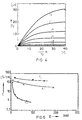
- Typical characteristics (Figs. 3, 4 respectively) of drain and gate current of a thin film transistor according to the present invention are satisfactory; curves a, b, c, d and e (Fig. 3) were measured at a drain voltage of 30, 20, 10, 6, 2 volt respectively; curves k, l, m, n, o and p (Fig. 4) at a gate voltage of 40, 35, 30, 25, 20 and 15 volt respectively.
- a power of 5W As a standardized preferred embodiment of the method according to the invention there is used a power of 5W, a pressure of 50m Torr, a SiH 4 flow of 20 sccm, a temperature of 300°C and 1% PH 3 in the SiH 4 flow.
- a power of 5W As a standardized preferred embodiment of the method according to the invention there is used a power of 5W, a pressure of 50m Torr, a SiH 4 flow of 20 sccm, a temperature of 300°C and 1% PH 3 in the SiH 4 flow.
- a SiH 4 flow As a standardized preferred embodiment of the method according to the invention there is used a power of 5W, a pressure of 50m Torr, a SiH 4 flow of 20 sccm, a temperature of 300°C and 1% PH 3 in the SiH 4 flow.
- a 10% HF solution For 10 seconds the substrate was dipped in a 10% HF solution, before applying the layer.
- annealing temperature of 630°C for three hours makes it possible to produce a thin film-transistor on Hoya BSi-glass, which remains solid at such temperature.
- Fig. 5 shows the achieved conductivity C of the source and drain regions as a function of thickness D.
- Line i joins measuring dots of the conductivity layer directly disposed on a glass plate
- line f joins measuring points of such a layer after being annealed
- line g shows the conductivity of a layer of silicon deposited on a polycrystalline substrate after a HF dip
- line h shows the conductivity after sequential annealing.
- the two triangles in Fig. 5 relate to two measurements on a a-Si:H layer annealed at 600°C, deposited on a sheet of glass and polycrystalline layer respectively. At this temperature the difference in conductivity is even more significent, since at 600°C less nuclei for crystallization are formed than at 630°C. The value of the conductivity was found to be independent of the duration of the annealing process, which duration was varied between 1-12 hours. The thickness of the layer was 20 nm.
- the reduction in conductivity of the layer at increasing thickness indicates a decreasing degree of crystalline structure of the layer at increasing distance from the polycristalline substrate. A certain minimal duration of the chemical influence of F ions appears to be desired.
- an explanation for further improvement of the conductivity according to the second embodiment is based on the assumption that the source and/or drain areas form larger polycrystalline grains spaced from the substrate, under amorphous-like deposition conditions and after annealing, than at microcrystalline-like deposition conditions.
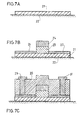
- FIG. 7A-7C Another comparative example not forming part of the present invention improves alignment of source and drain areas relatively to the gate, without using an additional mask step.
- a layer 21 of polycrystalline silicon was deposited on a quartz sheet 22 (Fig. 7A).
- a second mask (not shown) a gate insulator 23 (Fig. 7B) and a gate 24 of conducting or semiconducting material are provided.
- source and drain regions 26, 27 resp. were applied in a PECVD reactor under such conditions that no deposition was measurable onto the quartz plate 22 nor on the sides of the gate insulator 23. This was achieved by introducing SiF 4 into the PECVD reactor in a temperature range between 300-350 °C. At such temperatures Si-radicals were etched from a SiO 2 surface while deposited on a polysilicon foundation.
- a passivation layer 28 of SiO 2 and source and drain contacts 29, 31 respectively were applied, obtaining a thin film transistor having mutually aligned gate and source/drain-regions.
Landscapes
- Thin Film Transistor (AREA)
- Bipolar Transistors (AREA)
- Drying Of Semiconductors (AREA)
Abstract
Description
- The present invention relates to the production of thin film transistors in which the conductivity of source and/or drain regions should be high, e.g. for driving liquid crystal displays (LCD).
- From the prior art it is known to produce source and/or drain regions for a thin film transistor with a high conductivity, e.g. greater than or equivalent to 1 Ω -1 cm-1 by means of ion implantation. Such ion implantation is cumbersome, requires complicated equipment and is difficult to apply to relatively large surfaces. Further it is known from EP-A-0062079 to produce a semiconductive layer in microcrystalline form by means of a PECVD reactor.
- US patent 4625224 relates to a thin film transistor having 0.0001-5 atomic %Cℓ.
- EP-A-0161555 relates to a polycrystalline silicon thin film transistor structure having source and drain regions in amorphous form.
- Also US-A-4,485,121, EP-A-0232619 and GB-A-2156385 show structures using amorphous materials.
- Further the following publications are known to the applicant: EP-0132076, EP-0200552, EP-0201270, EP-0206649, EP-0206650, EP-0228295, EP-0228870, EP-0229518, EP-0229707, EP-0232148, EP-0234094, EP-0240305, EP-0240306, EP-0240314, EP-0241311, EP-0241316, EP-0241317, EP-0242207, EP-0243074; and article "Very-low Temperature Silicon Epitaxy by Plasma-DVD Using SiH4-PH3-H2 Reactants for Bipolar Devices" from the Japanese Journal of Applied Physics, Vol. 27, No. 4, April 1988, pages L493-L495.
- It is an object of the present invention to improve upon the above prior art.
- It is a further object of the present invention to produce a thin film transistor using relatively inexpensive equipment.
- It is a further object to produce a thin film transistor having high conductivity in source and drain regions at relatively low temperatures.
- Yet another object of the present invention is to produce a thin film transistor having such a high lateral conductivity in source and drain regions, that cross sectional areas of its source and drain contacts can be smaller than the cross sectional areas of the source and/or drain regions. This feature simplifies alignment in the production process and is of great importance for reducing the dimensions of such a thin film transistor.
- Another aspect relates to a depositing process in which a type of self-alignment is advantageously used.
- The present invention relates to a method according to
claim 1 of producing a thin film transistor, comprising the following steps: - depositing onto a non-silicon substrate a thin film of silicon semiconductor material, under such conditions that polycrystalline material is formed;
- depositing a doped silicon material on said film to form source and drain regions
- forming an insulating layer onto the transistor surface; and
- forming a gate electrode onto said insulating layer,
- Fluor (F) is used in the process, since F-ions show properties for etching an oxidized top layer. Furthermore the presence of F-ions may diminish the H content in a deposited layer which H content could prevent grains from growing.
- Further objects, features, details and advantages of the present invention will be clarified on the basis of the following disclosure in which preferred embodiments are illustrated with reference to the accompanying drawings, in which:
- Fig. 1 is a section view of a thin film transistor produced according to a method according to the present invention;
- Fig. 2 is a graph of the conductivity of the source and drain regions of a thin film transistor of fig. 1, related to the thickness of the layers applied according to the invention;
- Fig. 3 is a graph of the drain current, related to the gate voltage of the thin film transistor from fig. 1;
- Fig. 4 is a graph of the drain current of the thin film transistor from fig. 1, related to the drain voltage;
- Fig. 5 is a graph of the conductivity of the source and drain regions of the thin film transistor from fig. 1, produced according to the method according to the present invention;
- Fig. 6 a graph showing the conductivity of the source and drain regions of the thin film transistor from Fig. 1, produced according to a comparative example ; and
- Fig. 7A-7C show steps of producing the thin film transistor of Fig. 1 in accordance with a method of the invention.
- A
thin film transistor 2 disposed onto a sheet or plate 1 (Fig. 1) of glass or quartz is produced as follows: - A polycrystalline silicon bulk layer or a
thin film 8 is disposed in a LPCVD reactor (Low Pressure Chemical Vapour Deposition) in a direct or indirect way, indirectly meaning to firsty dispose an amorphous silicon layer at 550°C, after which annealing is executed at 630°C, whereby a grain size up to 400 nm is obtained; it is also possible to dispose such a polycrystalline layer in plasma enhanced CVD reactor. - Thereafter the polysilicon
thin film 8 is dipped in hydrogen fluoride (HF-dip), rinsed in a glove box using a N2 purge so as to diminish water and oxygen pollution of the system. It is apparent that other methods may be used to prevent water and oxygen pollution. - Next a layer is disposed under amorphous-like or microcrystalline-like deposition conditions in a PECVD reactor (Plasma Enhanced Chemical Vapour Deposition); and then such layer is selectively etched (Auto-Stop-Etching), such that source and
drain regions 3, 4 respectively are defined. - A gate insulator 9 of SiO2 is then disposed in a APCVD reactor (Atmospheric Pressure Chemical Vapour Deposition); for the skilled artison it is also apparent that, instead any other gate insulator may be used, such as silicon nitride. Onto such insulator a metal layer, e.g. of chromium (Cr), is disposed, from which after an etching step the gate 7 is produced. The gate may instead be of semiconductor material.
- Next, a covering
oxide layer 11 is disposed over the gate contact and the gate insulating layer 9; and finally contacts 5, 6 for connecting source, drain and/orgate regions 3, 4, 7 respectively of metal, e.g. aluminium, are disposed after providing holes therefor. - Producing source and drain regions was executed in a PD80 deposition system of Plasma Technology under circumstances according to the following table.
Amorphous-like Microcrystalline like Gasflow 1% PH3 in SiH4sccm 5-40 3-6 Gasflow H2 sccm 0 150 Rf-power W 5-10 30-50 Pressure (1 Torr = 133 Nm-2) mTorr 50-100 70 Temperature °C 250-450 250-450 - Tests show that disposing silicon under microcrystalline or amorphous conditions products a conductivity of said a layer that depends on the conductivity of the underlying layer. The curves of Fig. 2 illustrate this principle. Curves I and II show the increase of conductivity at increasing thickness of a layer disposed on a glass plate, at different grow rates, viz. 3.3 nm per minute and 1.3 nm per minute, respectively; curves III and IV show test results under microcrystalline-like disposition conditions in the plasma reactor, having a bulk layer of polysilicon as foundation, whereby again deposition rates of 3.3, 1.3 nm/minute respectively were used. Dots V and VI show two separate measurements of a thin layer slowly deposited, viz. at a rate of 0.12 nm/minute and 0.2 nm/minute respectively. The conductivity or resistance measurements used a fourpoint probe.
- Without limiting the invention, a plausible explanation of the differences between the curves of Fig. 2 is that epitaxial-like growth is produced and that polycrystalline information of the substrate is transmitted to the layer to be disposed thereon, whereby an accordingly lower resistance of at least a first part of that layer is produced. The crystalline structure of the upper layer is related to the crystalline structure of the lower layer.
- Typical characteristics (Figs. 3, 4 respectively) of drain and gate current of a thin film transistor according to the present invention are satisfactory; curves a, b, c, d and e (Fig. 3) were measured at a drain voltage of 30, 20, 10, 6, 2 volt respectively; curves k, l, m, n, o and p (Fig. 4) at a gate voltage of 40, 35, 30, 25, 20 and 15 volt respectively.
- An embodiment of the method according to
claim 1 of the invention for producing drain and/or source regions to be used in a structure shown in Fig. 1, uses amorphous deposition conditions, followed by annealing of the produced layer. - As a standardized preferred embodiment of the method according to the invention there is used a power of 5W, a pressure of 50m Torr, a SiH4 flow of 20 sccm, a temperature of 300°C and 1% PH3 in the SiH4 flow. For 10 seconds the substrate was dipped in a 10% HF solution, before applying the layer.
- An annealing temperature of 630°C for three hours makes it possible to produce a thin film-transistor on Hoya BSi-glass, which remains solid at such temperature. Fig. 5 shows the achieved conductivity C of the source and drain regions as a function of thickness D.
- Line i joins measuring dots of the conductivity layer directly disposed on a glass plate, line f joins measuring points of such a layer after being annealed, line g shows the conductivity of a layer of silicon deposited on a polycrystalline substrate after a HF dip and line h shows the conductivity after sequential annealing.
- The two triangles in Fig. 5 relate to two measurements on a a-Si:H layer annealed at 600°C, deposited on a sheet of glass and polycrystalline layer respectively. At this temperature the difference in conductivity is even more significent, since at 600°C less nuclei for crystallization are formed than at 630°C. The value of the conductivity was found to be independent of the duration of the annealing process, which duration was varied between 1-12 hours. The thickness of the layer was 20 nm.
- The reduction in conductivity of the layer at increasing thickness indicates a decreasing degree of crystalline structure of the layer at increasing distance from the polycristalline substrate. A certain minimal duration of the chemical influence of F ions appears to be desired.
- Without limiting the invention, an explanation for further improvement of the conductivity according to the second embodiment is based on the assumption that the source and/or drain areas form larger polycrystalline grains spaced from the substrate, under amorphous-like deposition conditions and after annealing, than at microcrystalline-like deposition conditions.
- The above results were achieved by means of a relatively simple plasma CVD reactor, which was sealed by means of O-rings; no ultra high vacuum is required; and the reactor used was relatively inexpensive.
- The results of a comparative example not forming part of the present invention (Fig. 6) were obtained by introducing a fluoridized SiH4 gas, or SiHnF4-n (n=1,2,3) into the PECVD apparatus. Curve rr relates to the position under microcrystalline conditions, as above mentioned; curve t relates to the preferred embodiment, as above described in which A-Si:H is annealed; and curve s relates to the third embodiment, in which SiH2F2 is introduced at a rate of 5 sccm, 1% PH3 in SiH4 is introduced at a rate of 1 sccm, H2 is introduced at a rate of 100 sccm, at a pressure of 3 Torr, a temperature between 250-350 °C and an applied power of 17-35 watts.
- Another comparative example not forming part of the present invention (Figs. 7A-7C) improves alignment of source and drain areas relatively to the gate, without using an additional mask step.
- By means of a first mask (not shown) a
layer 21 of polycrystalline silicon was deposited on a quartz sheet 22 (Fig. 7A). By means of a second mask (not shown) a gate insulator 23 (Fig. 7B) and agate 24 of conducting or semiconducting material are provided. - Thereafter source and drain
regions quartz plate 22 nor on the sides of thegate insulator 23. This was achieved by introducing SiF4 into the PECVD reactor in a temperature range between 300-350 °C. At such temperatures Si-radicals were etched from a SiO2 surface while deposited on a polysilicon foundation. - Next, by means of two consecutive masks a
passivation layer 28 of SiO2 and source anddrain contacts - Due to the absence of overlap between the
gate 24 and source and drainregions
Claims (3)
- A method of producing a thin film transistor, comprising the following steps:- depositing onto a non-silicon substrate (1) a thin film of silicon semiconductor material (8), under such conditions that polycrystalline material is formed;- depositing a doped silicon material on said film to form source (3) and drain (4) regions- forming an insulating layer (9) onto the transistor surface; and- forming a gate electrode (7) onto said insulating layer,characterized in that prior to introducing said
polycrystalline layer into the Plasma Enhanced Chemical Vapour Deposition (PECVD) apparatus, said layer is subjected to a HF dip and subsequently said source and drain regions are formed in a PECVD process, in which SiHnF4-n (n=0,1,2,3) is introduced in the PECVD apparatus, under conditions for depositing (i) microcrystalline material or (ii) amorphous material on a non-silicon substrate, the amorphous material being subjected to a subsequent annealing step, whereby said drain and source regions have a conductivity greater than or equal to 5 mhos·cm-1. - A method according to claim 1, in which the annealing step is performed at a temperature under 700°C.
- A method according to claim 1, in which SiHnF4-n is SiF4.
Applications Claiming Priority (2)
| Application Number | Priority Date | Filing Date | Title |
|---|---|---|---|
| NL8801379 | 1988-05-30 | ||
| NL8801379A NL8801379A (en) | 1988-05-30 | 1988-05-30 | METHOD FOR MANUFACTURING A THIN FILM TRANSISTOR AND SUCH A THIN FILM TRANSISTOR |
Publications (2)
| Publication Number | Publication Date |
|---|---|
| EP0344863A1 EP0344863A1 (en) | 1989-12-06 |
| EP0344863B1 true EP0344863B1 (en) | 1996-08-21 |
Family
ID=19852371
Family Applications (1)
| Application Number | Title | Priority Date | Filing Date |
|---|---|---|---|
| EP89201379A Expired - Lifetime EP0344863B1 (en) | 1988-05-30 | 1989-05-30 | A method of producing a thin film transistor |
Country Status (8)
| Country | Link |
|---|---|
| US (1) | US5102813A (en) |
| EP (1) | EP0344863B1 (en) |
| JP (1) | JPH02177368A (en) |
| KR (1) | KR0183964B1 (en) |
| AT (1) | ATE141715T1 (en) |
| CA (1) | CA1318417C (en) |
| DE (1) | DE68926980T2 (en) |
| NL (1) | NL8801379A (en) |
Families Citing this family (26)
| Publication number | Priority date | Publication date | Assignee | Title |
|---|---|---|---|---|
| US5366917A (en) * | 1990-03-20 | 1994-11-22 | Nec Corporation | Method for fabricating polycrystalline silicon having micro roughness on the surface |
| US5691249A (en) * | 1990-03-20 | 1997-11-25 | Nec Corporation | Method for fabricating polycrystalline silicon having micro roughness on the surface |
| US5318919A (en) * | 1990-07-31 | 1994-06-07 | Sanyo Electric Co., Ltd. | Manufacturing method of thin film transistor |
| US5403760A (en) * | 1990-10-16 | 1995-04-04 | Texas Instruments Incorporated | Method of making a HgCdTe thin film transistor |
| DE69131570T2 (en) * | 1990-11-16 | 2000-02-17 | Seiko Epson Corp., Tokio/Tokyo | Method of manufacturing a thin film semiconductor device |
| GB9114018D0 (en) * | 1991-06-28 | 1991-08-14 | Philips Electronic Associated | Thin-film transistor manufacture |
| US5424230A (en) * | 1992-02-19 | 1995-06-13 | Casio Computer Co., Ltd. | Method of manufacturing a polysilicon thin film transistor |
| US5409851A (en) * | 1992-05-04 | 1995-04-25 | Goldstar Co., Ltd. | Method of making a thin film transistor |
| CN100530569C (en) * | 1993-10-01 | 2009-08-19 | 株式会社半导体能源研究所 | Semiconductor device and a method for manufacturing the same |
| US5719065A (en) | 1993-10-01 | 1998-02-17 | Semiconductor Energy Laboratory Co., Ltd. | Method for manufacturing semiconductor device with removable spacers |
| DE4435461C2 (en) | 1993-10-06 | 2001-09-20 | Micron Technology Inc N D Ges | Thin film transistor and its manufacturing process |
| US5796116A (en) | 1994-07-27 | 1998-08-18 | Sharp Kabushiki Kaisha | Thin-film semiconductor device including a semiconductor film with high field-effect mobility |
| US5814529A (en) | 1995-01-17 | 1998-09-29 | Semiconductor Energy Laboratory Co., Ltd. | Method for producing a semiconductor integrated circuit including a thin film transistor and a capacitor |
| JP3440291B2 (en) * | 1995-05-25 | 2003-08-25 | 独立行政法人産業技術総合研究所 | Microcrystalline silicon thin film transistor |
| JP3416723B2 (en) * | 1995-05-25 | 2003-06-16 | 独立行政法人産業技術総合研究所 | Amorphous silicon thin film transistor and method of manufacturing the same |
| US6043507A (en) * | 1997-09-24 | 2000-03-28 | Micron Technology, Inc. | Thin film transistors and methods of making |
| GB9817745D0 (en) * | 1998-08-15 | 1998-10-14 | Philips Electronics Nv | Manufacture of electronic devices comprising thin-film circuit elements |
| US7402467B1 (en) * | 1999-03-26 | 2008-07-22 | Semiconductor Energy Laboratory Co., Ltd. | Method of manufacturing a semiconductor device |
| DE19935046C2 (en) * | 1999-07-26 | 2001-07-12 | Schott Glas | Plasma CVD method and device for producing a microcrystalline Si: H layer on a substrate and the use thereof |
| DE10052131C2 (en) * | 2000-10-20 | 2003-02-13 | Advanced Micro Devices Inc | Process for the production of field effect transistors with a completely self-adjusting technology |
| JP3989761B2 (en) | 2002-04-09 | 2007-10-10 | 株式会社半導体エネルギー研究所 | Semiconductor display device |
| US7038239B2 (en) | 2002-04-09 | 2006-05-02 | Semiconductor Energy Laboratory Co., Ltd. | Semiconductor element and display device using the same |
| JP3989763B2 (en) | 2002-04-15 | 2007-10-10 | 株式会社半導体エネルギー研究所 | Semiconductor display device |
| TWI270919B (en) * | 2002-04-15 | 2007-01-11 | Semiconductor Energy Lab | Display device and method of fabricating the same |
| US7256421B2 (en) | 2002-05-17 | 2007-08-14 | Semiconductor Energy Laboratory, Co., Ltd. | Display device having a structure for preventing the deterioration of a light emitting device |
| JP5594773B2 (en) * | 2010-09-30 | 2014-09-24 | 国立大学法人九州大学 | Selective film formation method, film formation apparatus, and structure |
Citations (1)
| Publication number | Priority date | Publication date | Assignee | Title |
|---|---|---|---|---|
| US4226898A (en) * | 1978-03-16 | 1980-10-07 | Energy Conversion Devices, Inc. | Amorphous semiconductors equivalent to crystalline semiconductors produced by a glow discharge process |
Family Cites Families (16)
| Publication number | Priority date | Publication date | Assignee | Title |
|---|---|---|---|---|
| JPS5767020A (en) * | 1980-10-15 | 1982-04-23 | Agency Of Ind Science & Technol | Thin silicon film and its manufacture |
| US4523214A (en) * | 1981-07-03 | 1985-06-11 | Fuji Photo Film Co., Ltd. | Solid state image pickup device utilizing microcrystalline and amorphous silicon |
| JPH0620122B2 (en) * | 1982-01-19 | 1994-03-16 | キヤノン株式会社 | Semiconductor element |
| JPS58219732A (en) * | 1982-06-16 | 1983-12-21 | Tokyo Inst Of Technol | Manufacture of fluorine contained amorphous semiconductor |
| US4737379A (en) * | 1982-09-24 | 1988-04-12 | Energy Conversion Devices, Inc. | Plasma deposited coatings, and low temperature plasma method of making same |
| JPH0693509B2 (en) * | 1983-08-26 | 1994-11-16 | シャープ株式会社 | Thin film transistor |
| JPS60200523A (en) * | 1984-03-26 | 1985-10-11 | Agency Of Ind Science & Technol | Manufacture of silicon thin film |
| US4769338A (en) * | 1984-05-14 | 1988-09-06 | Energy Conversion Devices, Inc. | Thin film field effect transistor and method of making same |
| US4670763A (en) * | 1984-05-14 | 1987-06-02 | Energy Conversion Devices, Inc. | Thin film field effect transistor |
| US4727044A (en) * | 1984-05-18 | 1988-02-23 | Semiconductor Energy Laboratory Co., Ltd. | Method of making a thin film transistor with laser recrystallized source and drain |
| US4597160A (en) * | 1985-08-09 | 1986-07-01 | Rca Corporation | Method of fabricating a polysilicon transistor with a high carrier mobility |
| JPH0746729B2 (en) * | 1985-12-26 | 1995-05-17 | キヤノン株式会社 | Method of manufacturing thin film transistor |
| GB2185758B (en) * | 1985-12-28 | 1990-09-05 | Canon Kk | Method for forming deposited film |
| JPS62271418A (en) * | 1986-05-20 | 1987-11-25 | Matsushita Electric Ind Co Ltd | Manufacture of amorphous silicon semiconductor element |
| US4762808A (en) * | 1987-06-22 | 1988-08-09 | Dow Corning Corporation | Method of forming semiconducting amorphous silicon films from the thermal decomposition of fluorohydridodisilanes |
| GB2215126B (en) * | 1988-02-19 | 1990-11-14 | Gen Electric Co Plc | Process for manufacturing a thin film transistor |
-
1988
- 1988-05-30 NL NL8801379A patent/NL8801379A/en not_active Application Discontinuation
-
1989
- 1989-05-29 CA CA000600932A patent/CA1318417C/en not_active Expired - Fee Related
- 1989-05-29 JP JP1137313A patent/JPH02177368A/en active Pending
- 1989-05-30 AT AT89201379T patent/ATE141715T1/en not_active IP Right Cessation
- 1989-05-30 EP EP89201379A patent/EP0344863B1/en not_active Expired - Lifetime
- 1989-05-30 KR KR1019890007274A patent/KR0183964B1/en not_active Expired - Fee Related
- 1989-05-30 US US07/358,952 patent/US5102813A/en not_active Expired - Fee Related
- 1989-05-30 DE DE68926980T patent/DE68926980T2/en not_active Expired - Fee Related
Patent Citations (1)
| Publication number | Priority date | Publication date | Assignee | Title |
|---|---|---|---|---|
| US4226898A (en) * | 1978-03-16 | 1980-10-07 | Energy Conversion Devices, Inc. | Amorphous semiconductors equivalent to crystalline semiconductors produced by a glow discharge process |
Non-Patent Citations (2)
| Title |
|---|
| Chemical Vapor Dep. for Microelectronics, by A. Sherman, Noyes Publ., N.J. 1987, USA * |
| Chemical Vapor Deposition for Microelectronics, by A. Sherman, Noyes Publ., N. J. 1987, USA. * |
Also Published As
| Publication number | Publication date |
|---|---|
| DE68926980T2 (en) | 1997-01-16 |
| ATE141715T1 (en) | 1996-09-15 |
| NL8801379A (en) | 1989-12-18 |
| JPH02177368A (en) | 1990-07-10 |
| KR900019245A (en) | 1990-12-24 |
| CA1318417C (en) | 1993-05-25 |
| EP0344863A1 (en) | 1989-12-06 |
| US5102813A (en) | 1992-04-07 |
| DE68926980D1 (en) | 1996-09-26 |
| KR0183964B1 (en) | 1999-03-20 |
Similar Documents
| Publication | Publication Date | Title |
|---|---|---|
| US5102813A (en) | Method of fabricating a thin film transistor | |
| EP0598409B1 (en) | A method of manufacturing a semiconductor device | |
| US5534445A (en) | Method of fabricating a polysilicon thin film transistor | |
| US5716857A (en) | Method for manufacturing a semiconductor device | |
| US5751050A (en) | Semiconductor device having a polysilicon resistor element with increased stability and method of fabricating same | |
| US20050233092A1 (en) | Method of controlling the uniformity of PECVD-deposited thin films | |
| US5318919A (en) | Manufacturing method of thin film transistor | |
| JPH0773101B2 (en) | Plasma enhanced chemical vapor deposition | |
| US5714415A (en) | Method of forming thin semiconductor film | |
| US7420202B2 (en) | Electronic device including a transistor structure having an active region adjacent to a stressor layer and a process for forming the electronic device | |
| EP0678907B1 (en) | Method for fabricating reverse-staggered thin-film transistor | |
| US6777354B2 (en) | Semiconductor device and method of manufacturing the same | |
| US6514803B1 (en) | Process for making an amorphous silicon thin film semiconductor device | |
| CA2090096C (en) | Semiconductor device having polysilicon thin-film | |
| KR100269021B1 (en) | Insulated gate field effect semiconductor device and manufacturing method thereof | |
| JP3494304B2 (en) | Method for manufacturing thin film semiconductor device | |
| JP3130661B2 (en) | Thin film transistor and method of manufacturing the same | |
| JP3025342B2 (en) | Thin film transistor and method for forming the same | |
| JP2003197636A (en) | Thin film semiconductor device and method of manufacturing the same | |
| JP3278237B2 (en) | Method for manufacturing thin film transistor | |
| JP3130659B2 (en) | Thin film transistor and method of manufacturing the same | |
| JPH0653503A (en) | Thin film transistor and fabrication thereof | |
| JPH05145074A (en) | Thin film transistor and manufacturing method thereof | |
| JP3193813B2 (en) | Thin film transistor and method of manufacturing the same | |
| JPH03108319A (en) | Manufacturing method of semiconductor device |
Legal Events
| Date | Code | Title | Description |
|---|---|---|---|
| PUAI | Public reference made under article 153(3) epc to a published international application that has entered the european phase |
Free format text: ORIGINAL CODE: 0009012 |
|
| AK | Designated contracting states |
Kind code of ref document: A1 Designated state(s): AT BE CH DE ES FR GB GR IT LI LU NL SE |
|
| 17P | Request for examination filed |
Effective date: 19900122 |
|
| 17Q | First examination report despatched |
Effective date: 19920512 |
|
| GRAG | Despatch of communication of intention to grant |
Free format text: ORIGINAL CODE: EPIDOS AGRA |
|
| GRAH | Despatch of communication of intention to grant a patent |
Free format text: ORIGINAL CODE: EPIDOS IGRA |
|
| GRAH | Despatch of communication of intention to grant a patent |
Free format text: ORIGINAL CODE: EPIDOS IGRA |
|
| GRAA | (expected) grant |
Free format text: ORIGINAL CODE: 0009210 |
|
| AK | Designated contracting states |
Kind code of ref document: B1 Designated state(s): AT BE CH DE ES FR GB GR IT LI LU NL SE |
|
| PG25 | Lapsed in a contracting state [announced via postgrant information from national office to epo] |
Ref country code: GR Free format text: LAPSE BECAUSE OF FAILURE TO SUBMIT A TRANSLATION OF THE DESCRIPTION OR TO PAY THE FEE WITHIN THE PRESCRIBED TIME-LIMIT Effective date: 19960821 Ref country code: IT Free format text: LAPSE BECAUSE OF FAILURE TO SUBMIT A TRANSLATION OF THE DESCRIPTION OR TO PAY THE FEE WITHIN THE PRESCRIBED TIME-LIMIT;WARNING: LAPSES OF ITALIAN PATENTS WITH EFFECTIVE DATE BEFORE 2007 MAY HAVE OCCURRED AT ANY TIME BEFORE 2007. THE CORRECT EFFECTIVE DATE MAY BE DIFFERENT FROM THE ONE RECORDED. Effective date: 19960821 Ref country code: LI Effective date: 19960821 Ref country code: CH Effective date: 19960821 Ref country code: ES Free format text: THE PATENT HAS BEEN ANNULLED BY A DECISION OF A NATIONAL AUTHORITY Effective date: 19960821 Ref country code: AT Effective date: 19960821 |
|
| REF | Corresponds to: |
Ref document number: 141715 Country of ref document: AT Date of ref document: 19960915 Kind code of ref document: T |
|
| REF | Corresponds to: |
Ref document number: 68926980 Country of ref document: DE Date of ref document: 19960926 |
|
| ET | Fr: translation filed | ||
| PG25 | Lapsed in a contracting state [announced via postgrant information from national office to epo] |
Ref country code: SE Effective date: 19961121 |
|
| REG | Reference to a national code |
Ref country code: CH Ref legal event code: PL |
|
| PG25 | Lapsed in a contracting state [announced via postgrant information from national office to epo] |
Ref country code: LU Free format text: LAPSE BECAUSE OF NON-PAYMENT OF DUE FEES Effective date: 19970531 |
|
| PLBE | No opposition filed within time limit |
Free format text: ORIGINAL CODE: 0009261 |
|
| STAA | Information on the status of an ep patent application or granted ep patent |
Free format text: STATUS: NO OPPOSITION FILED WITHIN TIME LIMIT |
|
| 26N | No opposition filed | ||
| PGFP | Annual fee paid to national office [announced via postgrant information from national office to epo] |
Ref country code: NL Payment date: 19980531 Year of fee payment: 10 |
|
| PGFP | Annual fee paid to national office [announced via postgrant information from national office to epo] |
Ref country code: BE Payment date: 19980617 Year of fee payment: 10 |
|
| PG25 | Lapsed in a contracting state [announced via postgrant information from national office to epo] |
Ref country code: BE Free format text: LAPSE BECAUSE OF NON-PAYMENT OF DUE FEES Effective date: 19990531 |
|
| BERE | Be: lapsed |
Owner name: INTERUNIVERSITAIR MICROELEKTRONICA CENTRUM VZW Effective date: 19990531 |
|
| PG25 | Lapsed in a contracting state [announced via postgrant information from national office to epo] |
Ref country code: NL Free format text: LAPSE BECAUSE OF NON-PAYMENT OF DUE FEES Effective date: 19991201 |
|
| NLV4 | Nl: lapsed or anulled due to non-payment of the annual fee |
Effective date: 19991201 |
|
| REG | Reference to a national code |
Ref country code: GB Ref legal event code: IF02 |
|
| PGFP | Annual fee paid to national office [announced via postgrant information from national office to epo] |
Ref country code: GB Payment date: 20040430 Year of fee payment: 16 |
|
| PGFP | Annual fee paid to national office [announced via postgrant information from national office to epo] |
Ref country code: FR Payment date: 20040527 Year of fee payment: 16 |
|
| PGFP | Annual fee paid to national office [announced via postgrant information from national office to epo] |
Ref country code: DE Payment date: 20040528 Year of fee payment: 16 |
|
| PG25 | Lapsed in a contracting state [announced via postgrant information from national office to epo] |
Ref country code: GB Free format text: LAPSE BECAUSE OF NON-PAYMENT OF DUE FEES Effective date: 20050530 |
|
| PG25 | Lapsed in a contracting state [announced via postgrant information from national office to epo] |
Ref country code: DE Free format text: LAPSE BECAUSE OF NON-PAYMENT OF DUE FEES Effective date: 20051201 |
|
| GBPC | Gb: european patent ceased through non-payment of renewal fee |
Effective date: 20050530 |
|
| PG25 | Lapsed in a contracting state [announced via postgrant information from national office to epo] |
Ref country code: FR Free format text: LAPSE BECAUSE OF NON-PAYMENT OF DUE FEES Effective date: 20060131 |
|
| REG | Reference to a national code |
Ref country code: FR Ref legal event code: ST Effective date: 20060131 |