EP0343608A2 - Vermittlungsanlagegerät für digitale Signale - Google Patents
Vermittlungsanlagegerät für digitale Signale Download PDFInfo
- Publication number
- EP0343608A2 EP0343608A2 EP89109290A EP89109290A EP0343608A2 EP 0343608 A2 EP0343608 A2 EP 0343608A2 EP 89109290 A EP89109290 A EP 89109290A EP 89109290 A EP89109290 A EP 89109290A EP 0343608 A2 EP0343608 A2 EP 0343608A2
- Authority
- EP
- European Patent Office
- Prior art keywords
- circuit
- lines
- input
- line
- output
- Prior art date
- Legal status (The legal status is an assumption and is not a legal conclusion. Google has not performed a legal analysis and makes no representation as to the accuracy of the status listed.)
- Granted
Links
- 238000003491 array Methods 0.000 abstract description 4
- 238000007493 shaping process Methods 0.000 abstract description 3
- 239000004065 semiconductor Substances 0.000 abstract description 2
- 230000000875 corresponding effect Effects 0.000 description 10
- 238000010586 diagram Methods 0.000 description 8
- 239000011159 matrix material Substances 0.000 description 4
- 230000001276 controlling effect Effects 0.000 description 2
- 238000000034 method Methods 0.000 description 2
- 238000012544 monitoring process Methods 0.000 description 2
- 230000008054 signal transmission Effects 0.000 description 2
- 239000000758 substrate Substances 0.000 description 2
- 241000270433 Varanidae Species 0.000 description 1
- 102100029469 WD repeat and HMG-box DNA-binding protein 1 Human genes 0.000 description 1
- 101710097421 WD repeat and HMG-box DNA-binding protein 1 Proteins 0.000 description 1
- 230000005856 abnormality Effects 0.000 description 1
- 238000002360 preparation method Methods 0.000 description 1
- 238000004321 preservation Methods 0.000 description 1
- 230000004044 response Effects 0.000 description 1
Images




Classifications
-
- H—ELECTRICITY
- H04—ELECTRIC COMMUNICATION TECHNIQUE
- H04Q—SELECTING
- H04Q11/00—Selecting arrangements for multiplex systems
- H04Q11/04—Selecting arrangements for multiplex systems for time-division multiplexing
Definitions
- the present invention relates to a digital signal exchange equipment for connecting a plurality of digital signal input circuit lines to an arbitory circuit line of a plurality of output circuit lines and to a circuit line selection control apparatus for selectively controlling a circuit line connection and for preventing a connection error at an exchange time.
- any input circuit line can be connected to any output circuit line by making a selective, switching connection to a predetermined switching element.
- a matrix type unit for controlling a crosspoint connection by the switching element requires a very large number of switching elements with an increase in the circuit lines and, furthermore, the switching of the switching elements is very complex to control. Since, in this case, an input digital signal has to be passed through a great many of switching elements until it is output from the exchange equipment, it is not possible to, due to a high-speed requirement for a digital signal to be transferred, disregard a delay of that signal when it passes through the switching elements.
- the switching elements use may be made of electronic switches (semiconductor switches) in which case the signal passage characteristics of this type of switches are generally not equal in terms of the delay of a signal at a time of a rise and a fall. For this reason, the input digital signal suffers a deformation with respect to time, each time it passes through the switching element, so that it has a very great deformation. This causes a difficulty in a signal identification.
- a circuit line selection control apparatus used in the conventional exchange equipment performs a selective switching among the many circuit lines in a time-division fashion and dynamically monitors the switching elements so that a connection error may be prevented.
- the select signal is multiplexed in a time-division fashion to conform to the characteristic of the digital signal transmitted and then input to the exchange equipment.
- the bit rate of the select signal after being multiplexed becomes an extremely high level. It is, therefore, not easy to implement such a system.
- the error connection preventing means works under dynamical control of the switching element, only after a switch connection has been achieved, and it is not preferable that it be employed for such a purpose.
- the conventional digital signal exchange equipment involves a high-speed requirement for transmitted digital signals as well as an increase in a signal delay among the circuit lines resulting from a large increase in the number of circuit lines. It is thus difficult to meet the high-speed requirement for digital signals as well as an increase in the number of circuit lines. Since the conventional circuit selection switching apparatus performs a selective switching among circuit lines, it is not easy to achieve it as a practical apparatus due to an extremely high bit rate of the select signal. Indeed in spite of the dynamic monitoring of the switches, the apparatus works only after a switch connection is achieved, failing to be manufactured as a fully practical apparatus.
- a first object of the present invention is to provide a digital signal exchange equipment which is simple in arrangement, easy in the control of a switching among circuit lines, uniform in a signal delay time among the circuit lines and can fully suppress deformation caused during a signal transmission whereby it is readily possible to achieve a high-speed requirement for transmitted digital signals as well as an increase in the number of the circuit lines.
- a second object of the present invention is to provide a circuit line selection control apparatus which can readily and positively provide a protection against a circuit line connection error when the digital signal exchange equipment is implemented according to the first object of the present invention.
- a selector module for a digital signal exchange equipment which is responsive to external select signals to switchingly connect an n number (n: a natural number) of input circuit lines to an m number (m: a natural number) of output circuit lines, which comprises: an m number of basic selection circuits each comprising a first selection section provided for the respective output circuit line and responsive to the external select signals to select one from an n number of first input lines and to connect it to one output line and a second selection section adapted to select one line from the output line of the first selection section and one second input line and to connect it to one output line which is as an output circuit line; and an input bus commonly connecting the n number of first input lines of said m number of basic selection circuits to said n number of input circuit lines.
- a digital signal exchange equipment responsive to external select signals to switchingly connect a k ⁇ n (k, n: a natural number) number of input circuit lines to an l ⁇ m (l, m: a natural number) number of output circuit lines, which comprises: a k ⁇ l number of selector modules each having an m number of basic selection circuits, responsive to said external select signals, for selecting one of an n number of first input lines and for selecting one line from the selected line and one second input line to connect it to one output line, and an input bus for making a common connection among the n number of first input lines of the respective basic selection circuit; and connecting means for connecting said selector modules as a k-column/l-row array, for connecting said selector modules to said input circuit lines which are divided into k units with those input circuit lines on each column as a respective unit, for connecting an m number of output lines to an m number of second input lines, for each row, of the next row selector module and for
- a digital signal exchange equipment further comprising control means provided within said basic selection circuit to allow the selection circuit to switchingly be controlled with j-bit (j: a natural number) select signals; control signal generating means, responsive to external circuit line designation information, for generating the j-bit select signals, for generating a parity signal and for outputting both signals as a control signal; a register for a control signal, provided for a corresponding basic selection circuit, for holding the control signal which is generated in said control signal generating means and for delivering a select signal which is held to a corresponding basic selection circuit; a first parity calculation circuit, provided for the corresponding register, for receiving a control signal which is held in that register and performing a parity checking and for delivering a first parity error signal when an error is detected at a time of parity checking.
- j-bit j: a natural number
- Figs. 1 to 6 are views showing a digital signal exchange equipment according to one embodiment of the present invention.
- Figs. 7 to 9 are views showing a selection switching control apparatus according to another embodiment of the present invention.
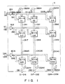
- Fig. 1 shows a whole arrangement of a 16 ⁇ 16-input/16 ⁇ 16-output type digital signal exchange equipment according to the present invention, noting that, here, a control system is omitted.
- S1 to S256 denote selector modules which constitute a 32-input/16-output (hereinafter referred as 32 ⁇ 16) type IC device having 16 inputs in a column direction and 16 outputs in a row direction.
- the IC device is formed, as a 16-columnx16-row array, on a substrate a.
- IB1 to IB16 show internal input buses which are provided to correspond to respective 16 circuit lines of 16 ⁇ 16 circuit lines of external input terminals, not shown.
- Digital signals which are input to external input terminals of respective 16 circuit lines are transmitted, respectively through bus drivers BD1 to DB16, to 16 selector modules S1 to S16, S17 to S32, ..., S241 to S256 on respective columns.
- CB1 to CB240 denote internal common buses and transmit 16 outputs of selector modules S l to S 16l on a l-th column to 16 inputs of selector modules S l+1 to S 16(l+1) on an(l+1)th column, noting that l denotes a natural number of 1 to 15.
- CB241 to CB256 are internal common buses and transmits 16 outputs of the selector modules S241 to S256 on the 16-th column to 16 inputs of selector modules S2 to S16 on the next column, noting that CB256 denotes an initial row.
- OB1 to OB16 are internal output buses and transmit 16 outputs of selector modules S241 to S256 on the column to corresponding external output terminals, not shown, of 16 ⁇ 16 circuit lines.
- An interface for control signal inputting/outputting, as well as a control bus for making a connection between the interface and the respective selector modules S1 to S256, is provided on the substrate a, though not shown in Fig. 1.
- the interface is connected to a host computer, not shown, and the respective selector modules S1 to S256 are selectively controlled by the host computer.
- the digital signal inputs I1 to I256 16 ⁇ 16 circuit lines are divided into 16 sections and are connected respectively through buffer drivers BD1 to BD16 to the internal input buses IB1 to IB16.
- the input digital signals of the internal input buses IB1 to IB16 are transmitted to the selector modules S1 to S16, S17 to S32, ..., S241 to S256.
- the respective selector modules S1, ..., S256 are arranged such that the input lines on the respective column are connected, in an normal state, to the corresponding output lines on the same column.
- the corresponding designated lines are selected for connection.
- a digital signal on the output line of a column is output to an outside via the internal output bus line of the same column, unless the first-mentioned line is selected by the other selector.
- Fig. 2 shows a detail of the 32 ⁇ 16 selector modules S where I1 to I16, C1 to C16, O1 to O16, and A0 to A4 denote internal input bus lines, internal common bus lines, internal output bus lines, and control bus lines, respectively.
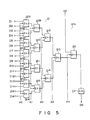
- the gate array Gm comprises a first 16 ⁇ 1 gate g1 for selecting one of the input bus lines II1 to II16, a second 2 ⁇ 1 gate g2 for selecting one of an output line of the first gate g1 and internal common bus line Cn (n: a natural number of 1 to 16) and connecting it to the internal output bus line On, and a timing circuit g3 constructed of a flip-flop (F/F) and adapted to obtain a coincidence output timing among the respective arrays G1 to G16.
- F/F flip-flop
- the first 16 ⁇ 1 gate g1 constitutes a tree-like array of 2 ⁇ 1 gates g01 to g15 with eight 2 ⁇ 1 gates g01 to g08 at a first stage, four 2 ⁇ 1 g09 to g12 at a second stage, two 2 ⁇ 1 gates g13 and g14 at a third stage and one 2 ⁇ 1 gate g15 at a fourth stage.
- the respective gates g01 to g08, g09 to g12, g13 to g14 and g15 are selectively controlled by select signals A0, A1, A2 and A4, respectively.
- the output of the first gate g1 is connected to the input of the second 2 ⁇ 1 gate g2.
- the respective gates g01 to g15 are so constructed that, for example, the upper lines are selected when a select signal is "0" and the lower lines in Fig. 5 are selected when the select signal is "1".
- a select signal A3A2A1A0
- a select signal A3A2A1A0
- the 2 ⁇ 1 gates g01 to g15 and g2 can be implemented by a logic circuit as shown in Fig. 6.
- A, B denote a digital signal input line
- C a control signal input line
- X a digital signal output line.
- the gate array Gm is constructed with the 2 ⁇ 1 gate as a fundamental element, the input signal can pass through the gates with an equal number of gate passages to obtain ready synchronization and ready selection control can be achieved with 5-bit select signals (A0 to A4).
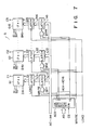
- Fig. 7 shows an arrangement of a control system for the aforementioned selector modules S.
- a control bus which is connected to the module S is constituted by the aforementioned five-bit select signal (A0 to A4), 4-bit address data AD, chip select signal cs, write instruction signal WRITE and load instruction signal LOAD.
- a control system comprises, for the respective gate array Gm, first and second latch circuits L1n and L2n and AND gates gan and address decoder ADD.
- a bus line of a 4-bit address data AD and chip select signal cs is connected to the address decoder ADD, and a bus line of an n channel output ADn of the address decoder ADD and write instruction signal WRITE is connected to the AND gate gan.
- the 5-bit bus line of the select signals A0 to A4 and output line of the AND gate gan are connected to the first latch circuit L1n; the 5-bit output line of the first latch circuit L1n and a bus line of a load instruction signal LOAD are connected to a second latch circuit L2n; and a 5-bit output terminal of the second latch circuit L2n is connected to a control bus of the respective gate array Gm.
- the aforementioned address decoder ADD is initiated upon receipt of a chip select signal cs and receives the 4-bit address data AD to identify which gate array Gm is designated, and transmits a designation signal ADn to the AND gate gan of the designated gate array Gm.
- the AND gate gan Upon receipt of the designated signal ADn, the AND gate gan supplies a write instruction signal WRITE to the first latch circuit L1n.
- the first latch circuit L1n receives the select signals A0 to A4. when it receives a write instruction signal WRITE, and holds them until it receives the next write instruction signal WRITE.
- the second latch circuit L2n Upon receipt of a load instruction signal LOAD, the second latch circuit L2n receives a latch output of the first latch circuit L1n and transmits it to the gate array Gm until the next instruction signal LOAD is received. By so doing, it is possible to make the first latch circuit L1n in a "freely writable" state and hold the next select signal for the respective gate array Gm.
- the digital signal exchange equipment thus arranged includes a combination of IC selector modules and can readily cope with an increase in their circuit lines. Furthermore, the exchange equipment allows the use of a simpler control system since it is possible to perform control per module. At the same time, since the respective modules are switchingly controlled by the output of the latch circuit and since the synchronization, as well as the shaping of a waveform, is achieved by the flip-flop circuit in the respective module, a circuit-to-circuit delay time becomes uniform and any possible deformation as generated during a signal transmission can be reduced to a satisfactory extent. As a result, adequate preparation can readily be made for the use of a high-speed digital signal as well as an increase in the circuit lines.
- Fig. 8 shows an arrangement of a checking circuit arrangement for the circuit line selection control apparatus of the present invention which is provided to meet the aforementioned need.
- the checking circuit arrangement is provided for the respective gate array Gm.
- identical reference numerals are employed to designate parts or elements corresponding to those shown in Fig. 7 and different parts or sections will be explained below.
- control bus To the aforementioned control bus are connected bus lines of a parity signal P, even/odd designation signal EVEN/ODD, read instruction signal READ and read switching signal RR, 6-line read output bus RB and write output bus WB (A0 to A4, P control bus lines) and bus lines for parity error signals PE1, PE2.
- the read output bus RB, write output bus WB and respective buses of the parity error signals PE1, PE2 are connected via their interface to an external host computer.
- the read output bus RB and write output bus WB may be provided as a single shared bus because a write and a read operation are not performed simultaneously.
- a 6-bit register is employed for the first and second latch circuits L1n and L2n.
- the first latch circuit L1n receives a write instruction signal from an AND gate gn and holds not only select signals A0 to A4 but also a parity signal P.
- the held signals A0 to A4 and P are output to a second latch L2n, first parity check circuit PC1 and switch circuit SW1.
- the second latch circuit L2n Upon receipt of a load instruction signal LOAD, the second latch circuit L2n supplies the output signals A0 to A4, P to the first latch circuit L1n to the second parity check circuit PC2 and second read switch circuit SW2, and only select signals A0 to A4 are fed to a gate array Gm.
- the first and second parity circuits PC1 to PC2 are of the same type and are constructed as shown, for example, in Fig. 9.
- g01 to g03 denote exclusive OR gates (hereinafter referred to as EX-OR gates) in which case signals A0 to A2 are supplied to the gate g01, signals A3, A4, P and EVEN/ODD are supplied to the gate g02 and the outputs of the gates g01 and g02 are supplied to the gate 03.
- EX-OR gates g01 and g02 are indicated as having three and four inputs, respectively, showing that the 2-input EX-OR gates are multi-connected to obtain the gates g01 and g02.
- the even/odd designation signal EVEN/ODD determines whether a parity signal is set as an even parity or an odd parity.
- the read instruction signal READ and read switching signal RR select the first and second read switch circuits SW1 and SW2 via the gates g1n to g3n, and the outputs of the switch circuits SW1 and SW2 are fed to the read output bus RB.
- the outputs of the gates g1n, g2n and g3n become “1", “1” and "0”, respectively, turning the first read switch circuit SW1 ON and the second read switch SW2 OFF.
- the outputs A0 to A4, P of the first latch circuit L1n are read onto the output bus RB.
- the select signals A0 to A4 and parity signal are sent to the latch circuit L1n and L2n.
- the respective outputs of the latch circuits L1n and L2n are parity-checked and, if an error occurs, error signals PE1, PE2 are sent to the host computer. It is thus possible to immedi strictlyately ascertains whether or not right select signals are held in the respective latch circuits L1n and L2n and to, if an error occurs, implement an interrupt processing for data preservation to be made by the host computer.
- the first and second latch circuits L1n and L2n Upon receipt of the read instruction signal READ and read switching signal RR, the first and second latch circuits L1n and L2n send the respective outputs A0 to A4, P to the read output bus RB as set forth above and from there onto the host computer.
- the host computer can sequentially monitor the memory contents in all of the latch circuits, thereby largely reducing a response time from the generation of an error to a corresponding action to be taken.
- circuit line selection switching control apparatus having the aforementioned checking circuit arrangement can readily and positively provide a protection against a connection error between the circuit lines.
Landscapes
- Engineering & Computer Science (AREA)
- Computer Networks & Wireless Communication (AREA)
- Use Of Switch Circuits For Exchanges And Methods Of Control Of Multiplex Exchanges (AREA)
Applications Claiming Priority (6)
| Application Number | Priority Date | Filing Date | Title |
|---|---|---|---|
| JP125125/88 | 1988-05-23 | ||
| JP12512588 | 1988-05-23 | ||
| JP12512588A JPH01293796A (ja) | 1988-05-23 | 1988-05-23 | デジタル信号交換器 |
| JP125124/88 | 1988-05-23 | ||
| JP12512488 | 1988-05-23 | ||
| JP12512488A JP2788250B2 (ja) | 1988-05-23 | 1988-05-23 | ディジタル信号交換器及びディジタル信号交換器の選択モジュール |
Publications (3)
| Publication Number | Publication Date |
|---|---|
| EP0343608A2 true EP0343608A2 (de) | 1989-11-29 |
| EP0343608A3 EP0343608A3 (de) | 1992-10-14 |
| EP0343608B1 EP0343608B1 (de) | 2000-03-08 |
Family
ID=26461645
Family Applications (1)
| Application Number | Title | Priority Date | Filing Date |
|---|---|---|---|
| EP19890109290 Expired - Lifetime EP0343608B1 (de) | 1988-05-23 | 1989-05-23 | Vermittlungsanlagegerät für digitale Signale |
Country Status (3)
| Country | Link |
|---|---|
| EP (1) | EP0343608B1 (de) |
| CA (1) | CA1332631C (de) |
| DE (1) | DE68929166T2 (de) |
Family Cites Families (2)
| Publication number | Priority date | Publication date | Assignee | Title |
|---|---|---|---|---|
| FR2430152A1 (fr) * | 1978-06-29 | 1980-01-25 | Duret Christian | Reseau nodal modulaire pour la commutation de signaux electriques, notamment de signaux de telecommunications |
| EP0165499B1 (de) * | 1984-06-12 | 1988-09-07 | Siemens Aktiengesellschaft | Raummultiplexkoppelnetz |
-
1989
- 1989-05-17 CA CA 599982 patent/CA1332631C/en not_active Expired - Fee Related
- 1989-05-23 EP EP19890109290 patent/EP0343608B1/de not_active Expired - Lifetime
- 1989-05-23 DE DE1989629166 patent/DE68929166T2/de not_active Expired - Lifetime
Also Published As
| Publication number | Publication date |
|---|---|
| EP0343608A3 (de) | 1992-10-14 |
| DE68929166D1 (de) | 2000-04-13 |
| EP0343608B1 (de) | 2000-03-08 |
| DE68929166T2 (de) | 2000-11-23 |
| CA1332631C (en) | 1994-10-18 |
Similar Documents
| Publication | Publication Date | Title |
|---|---|---|
| JP3241045B2 (ja) | マルチポート共有メモリインタフェースおよび関連の方法 | |
| EP0430569B1 (de) | Fehlertolerante Verbindungsnetze | |
| JPH01217575A (ja) | ビデオプロセッサシステム | |
| JPH0156595B2 (de) | ||
| JPH01232463A (ja) | データプロセッサシステムとそれを備えるビデオプロセッサシステム | |
| EP0843893B1 (de) | Mikrokontroller mit einer geringeren n-bit-datenbus-breite als anzahl i/o-ausgänge | |
| US6728256B1 (en) | Shared buffer control device | |
| US5555214A (en) | Apparatus for serial reading and writing of random access memory arrays | |
| US3991276A (en) | Time-space-time division switching network | |
| US5448572A (en) | Spare signal line switching method and apparatus | |
| US3763472A (en) | Distributing and collecting memory array and transfer system | |
| EP0343608A2 (de) | Vermittlungsanlagegerät für digitale Signale | |
| US5276439A (en) | Digital signal exchange equipment | |
| US4961159A (en) | Cellular automaton for generating random data | |
| US5572198A (en) | Method and apparatus for routing in reduced switch matrices to provide one hundred percent coverage | |
| US6470011B1 (en) | Time division multiplex highway switch control system and control method of T-S-T three-stage switches in electronic switching system | |
| JP2788250B2 (ja) | ディジタル信号交換器及びディジタル信号交換器の選択モジュール | |
| CN1013069B (zh) | 多通道控制器 | |
| JP2754885B2 (ja) | Cpu出力データ制御回路 | |
| US6526047B1 (en) | Single point writing of control information | |
| JPH01293796A (ja) | デジタル信号交換器 | |
| JP2613963B2 (ja) | データ入出力装置 | |
| JPS6362011B2 (de) | ||
| JPH02170745A (ja) | 広帯域デジタル交換装置 | |
| JPS59117618A (ja) | デ−タバス制御装置 |
Legal Events
| Date | Code | Title | Description |
|---|---|---|---|
| PUAI | Public reference made under article 153(3) epc to a published international application that has entered the european phase |
Free format text: ORIGINAL CODE: 0009012 |
|
| 17P | Request for examination filed |
Effective date: 19890620 |
|
| AK | Designated contracting states |
Kind code of ref document: A2 Designated state(s): DE FR GB |
|
| PUAL | Search report despatched |
Free format text: ORIGINAL CODE: 0009013 |
|
| AK | Designated contracting states |
Kind code of ref document: A3 Designated state(s): DE FR GB |
|
| 17Q | First examination report despatched |
Effective date: 19960530 |
|
| GRAG | Despatch of communication of intention to grant |
Free format text: ORIGINAL CODE: EPIDOS AGRA |
|
| GRAG | Despatch of communication of intention to grant |
Free format text: ORIGINAL CODE: EPIDOS AGRA |
|
| GRAH | Despatch of communication of intention to grant a patent |
Free format text: ORIGINAL CODE: EPIDOS IGRA |
|
| GRAH | Despatch of communication of intention to grant a patent |
Free format text: ORIGINAL CODE: EPIDOS IGRA |
|
| GRAA | (expected) grant |
Free format text: ORIGINAL CODE: 0009210 |
|
| AK | Designated contracting states |
Kind code of ref document: B1 Designated state(s): DE FR GB |
|
| REF | Corresponds to: |
Ref document number: 68929166 Country of ref document: DE Date of ref document: 20000413 |
|
| ET | Fr: translation filed | ||
| PLBE | No opposition filed within time limit |
Free format text: ORIGINAL CODE: 0009261 |
|
| STAA | Information on the status of an ep patent application or granted ep patent |
Free format text: STATUS: NO OPPOSITION FILED WITHIN TIME LIMIT |
|
| 26N | No opposition filed | ||
| REG | Reference to a national code |
Ref country code: GB Ref legal event code: IF02 |
|
| REG | Reference to a national code |
Ref country code: GB Ref legal event code: 746 Effective date: 20070317 |
|
| PGFP | Annual fee paid to national office [announced via postgrant information from national office to epo] |
Ref country code: DE Payment date: 20080529 Year of fee payment: 20 |
|
| PGFP | Annual fee paid to national office [announced via postgrant information from national office to epo] |
Ref country code: GB Payment date: 20080528 Year of fee payment: 20 |
|
| REG | Reference to a national code |
Ref country code: GB Ref legal event code: PE20 Expiry date: 20090522 |
|
| PG25 | Lapsed in a contracting state [announced via postgrant information from national office to epo] |
Ref country code: GB Free format text: LAPSE BECAUSE OF EXPIRATION OF PROTECTION Effective date: 20090522 |
|
| PGFP | Annual fee paid to national office [announced via postgrant information from national office to epo] |
Ref country code: FR Payment date: 20080514 Year of fee payment: 20 |