EP0343392A2 - Agencement pour l'affichage d'une quantité variable d'un semi-conducteur commandé - Google Patents
Agencement pour l'affichage d'une quantité variable d'un semi-conducteur commandé Download PDFInfo
- Publication number
- EP0343392A2 EP0343392A2 EP89107538A EP89107538A EP0343392A2 EP 0343392 A2 EP0343392 A2 EP 0343392A2 EP 89107538 A EP89107538 A EP 89107538A EP 89107538 A EP89107538 A EP 89107538A EP 0343392 A2 EP0343392 A2 EP 0343392A2
- Authority
- EP
- European Patent Office
- Prior art keywords
- input
- comparator
- output
- arrangement according
- designed
- Prior art date
- Legal status (The legal status is an assumption and is not a legal conclusion. Google has not performed a legal analysis and makes no representation as to the accuracy of the status listed.)
- Granted
Links
Images

Classifications
-
- G—PHYSICS
- G01—MEASURING; TESTING
- G01R—MEASURING ELECTRIC VARIABLES; MEASURING MAGNETIC VARIABLES
- G01R19/00—Arrangements for measuring currents or voltages or for indicating presence or sign thereof
- G01R19/0007—Frequency selective voltage or current level measuring
- G01R19/0015—Frequency selective voltage or current level measuring separating AC and DC
-
- G—PHYSICS
- G01—MEASURING; TESTING
- G01R—MEASURING ELECTRIC VARIABLES; MEASURING MAGNETIC VARIABLES
- G01R15/00—Details of measuring arrangements of the types provided for in groups G01R17/00 - G01R29/00, G01R33/00 - G01R33/26 or G01R35/00
- G01R15/14—Adaptations providing voltage or current isolation, e.g. for high-voltage or high-current networks
- G01R15/18—Adaptations providing voltage or current isolation, e.g. for high-voltage or high-current networks using inductive devices, e.g. transformers
- G01R15/183—Adaptations providing voltage or current isolation, e.g. for high-voltage or high-current networks using inductive devices, e.g. transformers using transformers with a magnetic core
- G01R15/185—Adaptations providing voltage or current isolation, e.g. for high-voltage or high-current networks using inductive devices, e.g. transformers using transformers with a magnetic core with compensation or feedback windings or interacting coils, e.g. 0-flux sensors
Definitions
- the invention relates to an arrangement for emulating an alternating variable, which has a direct component, in particular an alternating current, in a controlled semiconductor component with an electromagnetic transducer for measurement purposes.
- the invention has for its object to provide an arrangement of the type mentioned, with a tax th semiconductor component, the electrical alternating variable can be simulated in a simple manner for measuring, regulating and control functions with a direct component.
- a secondary winding of the converter is connected to an input of a sample and hold element, the trigger input of which is connected to a control device for the semiconductor component and trigger pulses from this control device in each case receives the control times of the semiconductor component, and that the output of the sample and hold element, whose output signal is proportional to the DC component, is routed to a first input of a comparator, the second input of which is connected to the secondary winding of the converter and at whose output the reproduced variable size is available.
- the comparator is a subtractor, the first input being designed as an inverting input and the second input as a non-inverting input.
- the simulated alternating variable also corresponds in its phase position to the original alternating variable.
- the inverting element and / or the comparator are preferably designed as amplifiers. An adjustment of the level relationships between the converter and the subsequent elements can thus be achieved, whereby the detection of even very small DC components is possible.
- a filter arrangement is arranged between the output of the comparator and a measuring output, which is designed as a blocking and low-pass filter.
- a measuring output which is designed as a blocking and low-pass filter.
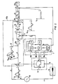
- FIG. 1 shows an arrangement 100 for emulating an alternating variable in a controlled semiconductor component, in particular a thyristor.
- a thyristor actuator 13 which forms a circuit with lines a, b, c, a load 14 and a voltage source 15.
- a current I T flows through the actuator 13 as shown.
- the semiconductor components 1 of the actuator 13 receive their control pulses from a control device 2.
- This control device 2 includes a pulse generator 24, the output pulses of which are passed on to the controlled semiconductors 1 via angle controls 23a, 23b and adaptation stages 18a, 18b.
- the current I T is detected by a converter 3.
- a voltage U W is transmitted as shown on its secondary side on the line d. It can be seen that the DC component is suppressed by the converter 3. The voltage time areas of the associated positive and negative half-waves are the same size. The original zero line 16 of the current profile I T is shifted downward by the amount 17 of the DC component.
- This voltage U W is fed via line d to an input 5 of a sample & hold element 4, the trigger input 6 of which is coupled to the control device 2. From the control device 2, the sample & hold element 4 receives trigger pulses each at the control times 20 of the semiconductor components 1.
- the comparator 9 is designed as a subtractor, the first input 8a being designed as an inverting input and the second input 8b as a non-inverting input. This means that the constant component U GL is subtracted from the alternating variable U W.
- the in-phase replica U IT of the ur change size I T is then used for further measurement purposes. It can be passed on, for example, to temperature monitors, monitoring and control devices or, as shown, to a measuring device 25 which displays the current value.
- FIG. 2 shows a further exemplary embodiment of the.
- the comparator 9 is designed as a summing element. So that the DC component with the correct polarity is summed with the converter signal, an inverting element 10 is arranged between the sample and hold element 4 and the comparator 9. Alternatively, an inverting element 10a can also be arranged at the input of the sample & hold element 4.
- the inverting element 10, 10a and / or the comparator 9 are preferably designed as amplifiers in order to achieve an optimal adaptation of the individual elements to one another.
- a filter 12 is arranged between the output 21 of the comparator 9 and a measuring output 22 and is designed as a blocking and low-pass filter. All alternating components of the voltage U IT are eliminated by the filter 12, so that a voltage U F is present at the measuring output 22 which is proportional to the entire DC component contained in the current I T. This can be routed, for example, via a line f to a control unit 19 of the control device 2 in order to achieve an undesired DC component in the load circuit by correcting the control times. This is of particular importance when the load 14 is inductive and an undesirable bias occurs.
- the voltage U F serves as a measure of the premagnetization. Alternatively, the voltage can also be supplied to monitoring devices or, as shown, to a measuring device 25a.
- An essential advantage of the arrangement 100 or 100a is that only the DC component is detected by the sample and hold element 4, which is not transmitted by the converter 3. This means that, for example, briefly dynamically occurring components that the converter 3 can be transmitted, not detected by the sample and hold element 4. In contrast to the signal U W, they have no shift in the alternating variable on the secondary side of the converter 3 over time. Dynamic components are therefore specifically taken into account and, if necessary, can be treated further in the filter arrangement 12.
Landscapes
- Engineering & Computer Science (AREA)
- Power Engineering (AREA)
- Physics & Mathematics (AREA)
- General Physics & Mathematics (AREA)
- Measurement Of Current Or Voltage (AREA)
- Rectifiers (AREA)
- Power Conversion In General (AREA)
Applications Claiming Priority (2)
| Application Number | Priority Date | Filing Date | Title |
|---|---|---|---|
| DE3815849 | 1988-05-09 | ||
| DE3815849 | 1988-05-09 |
Publications (3)
| Publication Number | Publication Date |
|---|---|
| EP0343392A2 true EP0343392A2 (fr) | 1989-11-29 |
| EP0343392A3 EP0343392A3 (en) | 1989-12-06 |
| EP0343392B1 EP0343392B1 (fr) | 1992-09-23 |
Family
ID=6354011
Family Applications (1)
| Application Number | Title | Priority Date | Filing Date |
|---|---|---|---|
| EP89107538A Expired - Lifetime EP0343392B1 (fr) | 1988-05-09 | 1989-04-26 | Agencement pour l'affichage d'une quantité variable d'un semi-conducteur commandé |
Country Status (5)
| Country | Link |
|---|---|
| US (1) | US4904925A (fr) |
| EP (1) | EP0343392B1 (fr) |
| JP (1) | JPH01320474A (fr) |
| CA (1) | CA1313224C (fr) |
| DE (1) | DE58902321D1 (fr) |
Cited By (1)
| Publication number | Priority date | Publication date | Assignee | Title |
|---|---|---|---|---|
| EP0494629A3 (en) * | 1991-01-08 | 1992-10-21 | Canon Kabushiki Kaisha | Electric power source |
Families Citing this family (1)
| Publication number | Priority date | Publication date | Assignee | Title |
|---|---|---|---|---|
| FR2870351B1 (fr) * | 2004-05-14 | 2006-07-14 | Alstom Transport Sa | Dispositif de mesure d'un champ electromagnetique, systeme de commande utilisant ce dispositif et circuit electronique concu pour ce dispositif |
Family Cites Families (7)
| Publication number | Priority date | Publication date | Assignee | Title |
|---|---|---|---|---|
| US28851A (en) * | 1860-06-26 | Improvement in sewing-machines | ||
| USRE28851E (en) | 1973-05-31 | 1976-06-08 | General Electric Company | Current transformer with active load termination |
| AU521914B2 (en) * | 1978-02-28 | 1982-05-06 | Tokyo Shibaura Denki Kabushiki Kaisha | Controlling electric valves in ac power supply |
| US4278940A (en) * | 1979-04-25 | 1981-07-14 | General Electric Company | Means for automatically compensating DC magnetization in a transformer |
| US4255705A (en) * | 1979-09-24 | 1981-03-10 | General Electric Company | Peak detection and electronic compensation of D. C. saturation magnetization in current transformers used in watt hour meter installations |
| US4255704A (en) * | 1979-10-01 | 1981-03-10 | General Electric Company | Zero crossing detection and electronic compensation of D. C. saturation magnetization in current transformers used in watthour meter installations |
| DD250051A1 (de) * | 1986-06-19 | 1987-09-30 | Medizin Labortechnik Veb K | Verfahren und schaltung zur automatischen nullpunktkorrektur taktgesteuerter messsysteme |
-
1989
- 1989-04-26 EP EP89107538A patent/EP0343392B1/fr not_active Expired - Lifetime
- 1989-04-26 DE DE8989107538T patent/DE58902321D1/de not_active Expired - Lifetime
- 1989-05-02 US US07/346,478 patent/US4904925A/en not_active Expired - Fee Related
- 1989-05-02 JP JP1113547A patent/JPH01320474A/ja active Pending
- 1989-05-05 CA CA000598777A patent/CA1313224C/fr not_active Expired - Fee Related
Cited By (2)
| Publication number | Priority date | Publication date | Assignee | Title |
|---|---|---|---|---|
| EP0494629A3 (en) * | 1991-01-08 | 1992-10-21 | Canon Kabushiki Kaisha | Electric power source |
| US5532913A (en) * | 1991-01-08 | 1996-07-02 | Canon Kabushiki Kaisha | Electric power source |
Also Published As
| Publication number | Publication date |
|---|---|
| DE58902321D1 (de) | 1992-10-29 |
| CA1313224C (fr) | 1993-01-26 |
| EP0343392A3 (en) | 1989-12-06 |
| EP0343392B1 (fr) | 1992-09-23 |
| JPH01320474A (ja) | 1989-12-26 |
| US4904925A (en) | 1990-02-27 |
Similar Documents
| Publication | Publication Date | Title |
|---|---|---|
| DE4230939C2 (de) | Schaltungsanordnung zum Ändern oder Prüfen elektrischer Eigenschaften eines Stromwandlers mit Magnetfeldkompensation | |
| EP0386604A2 (fr) | Compteur électrique statique | |
| EP1664804B1 (fr) | Procede et dispositif de mesure de tension | |
| DE29506883U1 (de) | Stromsensor nach dem Kompensationsprinzip | |
| DE3779749T2 (de) | Schaltung zum messen des die primaerwicklung des ausgangstransformators eines wechselrichters durch fliessenden gleichstromanteiles. | |
| DE3531869A1 (de) | Elektromagnetischer stroemungsmesser | |
| EP0150814A2 (fr) | Relais à impédance digital | |
| DE69305911T2 (de) | Einrichtung zur Überwachung eines homopolaren Fehlers im Stromnetz | |
| DE69333695T2 (de) | Schaltung zur Leistungsberechnung | |
| DE68918305T2 (de) | Schalter. | |
| EP0343392B1 (fr) | Agencement pour l'affichage d'une quantité variable d'un semi-conducteur commandé | |
| DE29507675U1 (de) | Kompensationsstromwandlung | |
| EP0686850A1 (fr) | Circuit de mesure de courants continus avec isolation de tension entre le circuit de courant et le circuit de mesure | |
| DE2603212A1 (de) | Kraftflussmessgeraet | |
| DE2716605C2 (de) | Schaltungsanordnung zur ErdschluBerfassung bei einem Stromrichter | |
| EP0250028A2 (fr) | Dispositif de montage pour la compensation de dérivés dépendants ou non de la température d'un capteur capacitif | |
| DE3329726C1 (de) | Kapazitäts- und Verlustfaktor-Meßbrücke | |
| DE2261953B2 (de) | Stromwandler zur Messung von Stromstärken, insbesondere in Hochspannungsleitungen | |
| DE4403077C2 (de) | Schaltungsanordnung für einen Wechselstromwandler und Verfahren zum Betrieb | |
| DE2508033A1 (de) | Kapazitaets- und verlustfaktormesseinrichtung mit selbsttaetiger abgleichung | |
| DE3143669A1 (de) | Schaltung zum messen des effektivwertes einer wechselspannung | |
| DE2527933C2 (de) | Verfahren und Schaltungsanordnung zum störwechselspannungsunabhängigen Ermitteln von Fremd-Gteichspannungen in Fernmelde-, insbesondere Fernsprechanlagen | |
| DE4318502C1 (de) | Verfahren und Schaltung zur Überwachung der Ströme von Leistungskondensatoren zur Blindleistungskompensation | |
| DE1908382A1 (de) | Gleichrichtende elektrische Schaltung | |
| DE3149990A1 (de) | Elektrische waage |
Legal Events
| Date | Code | Title | Description |
|---|---|---|---|
| PUAI | Public reference made under article 153(3) epc to a published international application that has entered the european phase |
Free format text: ORIGINAL CODE: 0009012 |
|
| PUAL | Search report despatched |
Free format text: ORIGINAL CODE: 0009013 |
|
| AK | Designated contracting states |
Kind code of ref document: A2 Designated state(s): CH DE FR GB LI SE |
|
| AK | Designated contracting states |
Kind code of ref document: A3 Designated state(s): CH DE FR GB LI SE |
|
| 17P | Request for examination filed |
Effective date: 19900509 |
|
| 17Q | First examination report despatched |
Effective date: 19920226 |
|
| GRAA | (expected) grant |
Free format text: ORIGINAL CODE: 0009210 |
|
| AK | Designated contracting states |
Kind code of ref document: B1 Designated state(s): CH DE FR GB LI SE |
|
| REF | Corresponds to: |
Ref document number: 58902321 Country of ref document: DE Date of ref document: 19921029 |
|
| GBT | Gb: translation of ep patent filed (gb section 77(6)(a)/1977) | ||
| ET | Fr: translation filed | ||
| PG25 | Lapsed in a contracting state [announced via postgrant information from national office to epo] |
Ref country code: LI Effective date: 19930430 Ref country code: CH Effective date: 19930430 |
|
| PLBE | No opposition filed within time limit |
Free format text: ORIGINAL CODE: 0009261 |
|
| STAA | Information on the status of an ep patent application or granted ep patent |
Free format text: STATUS: NO OPPOSITION FILED WITHIN TIME LIMIT |
|
| 26N | No opposition filed | ||
| PG25 | Lapsed in a contracting state [announced via postgrant information from national office to epo] |
Ref country code: FR Effective date: 19931229 |
|
| REG | Reference to a national code |
Ref country code: CH Ref legal event code: PL |
|
| REG | Reference to a national code |
Ref country code: FR Ref legal event code: ST |
|
| EAL | Se: european patent in force in sweden |
Ref document number: 89107538.4 |
|
| PGFP | Annual fee paid to national office [announced via postgrant information from national office to epo] |
Ref country code: SE Payment date: 19960410 Year of fee payment: 8 |
|
| PG25 | Lapsed in a contracting state [announced via postgrant information from national office to epo] |
Ref country code: SE Effective date: 19970427 |
|
| PGFP | Annual fee paid to national office [announced via postgrant information from national office to epo] |
Ref country code: DE Payment date: 19970617 Year of fee payment: 9 |
|
| EUG | Se: european patent has lapsed |
Ref document number: 89107538.4 |
|
| PGFP | Annual fee paid to national office [announced via postgrant information from national office to epo] |
Ref country code: GB Payment date: 19980310 Year of fee payment: 10 |
|
| PG25 | Lapsed in a contracting state [announced via postgrant information from national office to epo] |
Ref country code: DE Free format text: LAPSE BECAUSE OF NON-PAYMENT OF DUE FEES Effective date: 19990202 |
|
| PG25 | Lapsed in a contracting state [announced via postgrant information from national office to epo] |
Ref country code: GB Free format text: LAPSE BECAUSE OF NON-PAYMENT OF DUE FEES Effective date: 19990426 |
|
| GBPC | Gb: european patent ceased through non-payment of renewal fee |
Effective date: 19990426 |