EP0342821A2 - Kompensationsschaltung für elektronische Uhren - Google Patents
Kompensationsschaltung für elektronische Uhren Download PDFInfo
- Publication number
- EP0342821A2 EP0342821A2 EP89304501A EP89304501A EP0342821A2 EP 0342821 A2 EP0342821 A2 EP 0342821A2 EP 89304501 A EP89304501 A EP 89304501A EP 89304501 A EP89304501 A EP 89304501A EP 0342821 A2 EP0342821 A2 EP 0342821A2
- Authority
- EP
- European Patent Office
- Prior art keywords
- circuit
- driving
- detecting
- actuator
- electronic timepiece
- Prior art date
- Legal status (The legal status is an assumption and is not a legal conclusion. Google has not performed a legal analysis and makes no representation as to the accuracy of the status listed.)
- Ceased
Links
Images

Classifications
-
- G—PHYSICS
- G04—HOROLOGY
- G04C—ELECTROMECHANICAL CLOCKS OR WATCHES
- G04C3/00—Electromechanical clocks or watches independent of other time-pieces and in which the movement is maintained by electric means
- G04C3/14—Electromechanical clocks or watches independent of other time-pieces and in which the movement is maintained by electric means incorporating a stepping motor
- G04C3/143—Means to reduce power consumption by reducing pulse width or amplitude and related problems, e.g. detection of unwanted or missing step
Definitions
- This invention relates to compensating circuits for electronic timepieces, e.g. electronic watches, for example, for compensating discrepancy between time indications of an analog electronic timepiece which makes a sweep movement of a seconds hand.
- One typical conventional electronic watch is, as disclosed in Japanese Patent Publication No. 47512/1981, such that intermittent rotational energy is accumulated by magnetic attraction of a driving magnet 71 engaging, as illustrated in Figure 2, with a fourth pinion 15b as well as a driving magnet 73 immersed in a viscous fluid 74. Viscous resistance of a receiver 76 and the driven magnets 73 act to smooth the rotation of the latter. In this case, the driven magnet 73 interlocks with a follower magnet 72 due to the magnetic attraction, with the result that a seconds hand spindle 15a is smoothly driven.
- a cap 75 functions to seal the viscous fluid.
- a driving circuit is of the low power consumption type, for example, disclosed in Japanese Patent Publications Nos. 75520/1979, 77162/1979 and 87977/1980.
- This conventional electronic watch has the following inherent problems.
- the amount of angular deviation between the magnets 72, 73 varies due to the fact that the viscosity of the viscous fluid 74 changes with change of temperature, or when the load of a calendar wheel train is applied.
- the variations in angular deviation in turn, cause discrepancy between time indications. Therefore, the resulting errors decrease accuracy of the time indication of the electronic watch.
- the present invention seeks to provide a compensating circuit for an electronic watch which compensating circuit is capable of compensating discrepancy between time indications by increasing or decreasing the number of repetitions of driving of an actuator by detecting variations in inverse induced voltage that are concomitant with fluctuations of load on the actuator.
- a compensating circuit for an electronic timepiece characterised by comprising: a clock circuit for intermittently driving an actuator, said clock circuit including at least a detecting circuit for detecting inverse induced voltages of said actuator; and a pulse number controlling circuit for increasing or decreasing the number of operations of driving said actuator in conformity with a judgement made by said detecting circuit.
- the compensating circuit may include means for changing the energy of signals for driving said actuator in such a direction as to have greater magnitudes as the load increases on the basis of the judgement of said detecting circuit.
- Said pulse number controlling circuit may include a variable frequency dividing means for making a frequency dividing ratio variable in accordance with a judgement signal of said detecting circuit.
- Said pulse number controlling circuit may include means for selectively changing over and connecting capacitors constituting an oscillation circuit of the electronic watch in accordance with the judgement signal of said detecting circuit.
- an electronic timepiece including a compensating circuit according to the present invention.
- the electronic timepiece may include storage means for storing intermittent rotational energy generated by the actuator, said storage means comprising a hair spring.
- the electronic timepiece may include controlling means for driving a time indicating hand smoothly, said controlling means being composed of a rotor immersed in a viscous fluid.
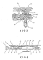
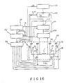
- FIG. 4 is a sectional view depicting a wheel train unit of the electronic watch of Figure 3.
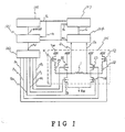
- a step motor serving as an actuator has a stator 4, a magnetic core 2, a rotor 5 and a coil 1.
- An accumulating means comprises a hair spring 10 for accumulating rotational energy in the form of elastic deformation.
- Control means comprises a viscous rotor 14 subject to viscous load imposed by a viscous fluid 17 ( Figure 4).
- Reference numeral 21 designates a base plate and reference numeral 22 denotes a wheel train receiver.
- the coil 1 generates a magnetic field for driving the rotor 5 through the magnetic core 2 and the stator 4.
- the coil 1, fixed by a screw 3, acts to drive a hair wheel 9 connected by means of a hair spring pinion 11 and also the hair spring 10 to a sixth pinion 6, a fifth gear 7 and fifth pinion 8, thereby driving a fourth wheel 15 with which a seconds hand 16 engages via a fourth idler 12.
- a viscous rotor idler 18 Interposed between the hair wheel 9 and the viscous rotor 14 for regulating the fourth wheel 15 is a viscous rotor idler 18 to increase the versatility in terms of layout. In this configuration, hours and minutes hands can be adjusted in co-operation with the pinion 11, the fourth idler 12, the viscous rotor idler 18, a date rear wheel 23 for driving the hours hands and a small iron wheel 24 meshing with a clutch wheel 37.
- the centre of the clutch wheel 37 has a substantially square opening and is slidable in a longitudinal direction along a square shaft of a winding stem 32.
- the clutch wheel 37 engages the square shaft of the winding stem 32 and thereby rotates in the same direction as the winding stem 32.
- a yoke 30 is subjected to a clockwise turning force by a spring (not shown).
- the yoke 30 engages a groove of the clutch wheel 37 to position the clutch wheel 37 so as to mesh with a setting wheel 24.
- the wheel 24 is coupled to the fourth wheel 15 through a minutes wheel 23.
- the minutes wheel 23 serves to drive the hours hand.
- a third wheel 25 decelerates the movement of the fourth wheel 15 with which the seconds hand is engaged and also drives the minutes hand.
- An IC 33 incorporates the compensating circuit according to the present invention.
- a quartz oscillator 35 supplies the coil 1 with driving waveforms for actuating the rotor 5 of the step motor.
- Reference numeral 36 represents a battery.
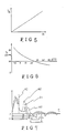
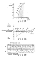
- Figure 5 is a graph showing one example of the relation between the storing torque Tk and winding angle ⁇ of the hair spring 10, whereing a spring constant K is approximately 0.4 mg.mm/deg, and the rotation is 3 rpm.
- Figure 6 is a graph illustrating one example of the relationship between load torque Tr and temperature ⁇ of the viscous rotor 14, wherein the values are obtained when setting rotational frequency at approximately 2 rpm.
- the load is about 40 mg.mm at a temperature of 25°C, about 85 mg.mm at -10°C and approximately 25 mg.mm at 50°C.
- the winding angle is proportional to the load.
- the angle is some 67° at 25°C but is approximately 140° at -10°C.
- the difference of 73° therebetween implies a delay of some 4 seconds with respect to the seconds hand as compared with the temperature of 25°C. Whereas at a temperature of 50°C, an advance of 1.4 seconds can be seen.
- Figure 7 is a waveform diagram showing an example of voltage waveforms when converting into a voltage an electric current flowing through the coil 1 when driving the step motor.
- the reference numeral 40 represents the voltage waveform at 0°C; reference numeral 41 represents the voltage waveform at 20°C; and the reference numeral 42 represents the voltage waveform at 40°C.
- the ordinate indicates an induced voltage v
- the abscissa indicates time t . Accordingly, as temperature increases, i.e. the load is reduced, the level of the inverse induced voltage v after termination of application of a driving pulse at point 43 is relatively large, whereas time t decreases. It is, therefore, possible to recognise load condition on the step motor by detecting the inverse induced voltage waveforms.
- Waveform 42 shows the case where the load is small, and the amplification of the induced voltage is large, thereby making the timing of the peak (turning off) point of the induced voltage earlier.
- Waveform 41 shows the middle degree of load.
- Waveform 40 shows a large load, and because of a small amplitude of oscillation of the rotor, the induced voltage is reduced, thereby making the time of the peak point of the induced voltage later. Accordingly, by the amplitude and timing of the induced voltage it is possible to know the relative load on the rotor.
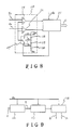
- a timer circuit consists of an oscillator circuit 100, a frequency dividing circuit 101, a motor driving pulse/detecting pulse forming circuit 102 and a motor driver/detecting voltage generation circuit 105.
- the oscillating circuit 100 generates standard signals ⁇ 32768 each having a frequency of 32768 Hz with the quartz oscillator 35 serving as a source of oscillation.
- the frequency dividing circuit 101 sequentially divides the frequencies of the standard signals 0 ⁇ 32768 to produce an output 0 ⁇ d, as a result of which the motor driving pulse/detecting pulse forming circuit 102 generates driving pulses P1, P2, inverted waveforms N1, N2 of the driving pulses P1, P2 and detecting pulses D1, D2 in order to drive the motor driver/detecting voltage generation circuit 105.
- Reference numerals 51, 52, 53, 55 represent P channel MOSFETs, and reference numerals 54, 56 designate N channel MOSFETs.
- the coil 1 is supplied with electric current alternately by simultaneously turning ON a group of MOSFETs 53, 56 or a group of MOSFETs 54, 55, thus driving the step motor.
- the inverse induced current generated in the coil 1 is forced to flow via a detecting resistor 58 or 57 to ground by turning the P channel MOSFETs 51, 52 ON whilst effecting a chopping process with the detecting pulses D1, D2.
- a detecting circuit 104 detects the load condition on the step motor from the voltage levels or the waveforms of the inverse induced voltages S1, S2 and emits detecting signals C to a pulse number control circuit 103.
- the pulse number control circuit 103 transmits control signals Po and Pd for increasing or decreasing the number of pulses in accordance with the detecting signals C, thereby controlling the oscillation circuit 100 and the frequency dividing circuit 101. The number of operations of driving the step motor per unit hour is thus increased or decreased.
- Watch signals 0 ⁇ c, 0 ⁇ d control the operations of the detecting circuit 104 and the pulse number control circuit 103.
- FIG. 8 is a block diagram showing the detecting circuit 104.
- a detecting unit 110 and a control unit 111 co-operate to convert the analog inverse induced voltages S1, S2 into digital values preparatory to the formation of the detecting signals C.
- the control unit 111 serves to impress on comparators 115, 116 reference voltages v1, v2, v3 obtained by dividing a power source voltage V DD by means of dividing resistors 118, 119, 120 whilst controlling and changing over a change over switch 117.
- the comparators 115, 116 compare the inverse induced voltages S1, S2 with the reference voltages v1, v2, v3, and further judge the voltage values of the inverse induced voltages S1, S2.
- the detecting signals C are produced by the control unit 111 in accordance with this comparison.
- the comparison employs three voltage levels v1, v2, v3, however, the comparison may employ more or less voltage levels.
- the circuitry is also not confined to that illustrated in Figure 8.
- the detection may target not only the voltage levels but also the timings at which the inverse induced voltages are generated or these timings in combination with the voltage levels. Namely, the detecting method may be diversified on the condition that the variation of inverse induced voltages with load is to be detected.
- FIG. 9 is a block diagram of the pulse number controlling circuit 103.
- the pulse number controlling circuit is composed of a de-coder 112 for transmitting a necessary correction quantity ⁇ by de-coding the magnitude of load and an indication of delay of the seconds hand from the detecting signals C, a memory 113 for storing the correction quantity ⁇ and a pulse forming unit 114 for producing the controlling signals Po, Pd for controlling the number of pulses serving to drive the step motor in accordance with the correction quantity.
- the de-coder 112 also functions to prevent malfunction caused due to instantaneous fluctuations in load such as impulses or external shock.
- the correction quantity ⁇ is temporarily stored in the memory 113, whereby the number of pulses for driving the step motor is gradually increased or decreased.
- the memory 113 also has the function of returning the stored correction quantity when the load reverts to its original state.
- the pulse forming unit 114 generates the control signals Po, Pd for increasing or decreasing the number of repetitions of driving the step motor depending on the pulse length or the pulse number in accordance with the correction quantity.
- clock pulses 0 ⁇ c control the operations of the respective components and serve as the reference for generating the timings of the control signals Pd, Po and also providing the pulse number for forming the pulse width.
- the correction quantity ⁇ stored in the memory 113 is increased or decreased on the basis of the load and the time.
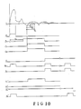
- Figure 10 is a timing chart showing an example of the operation of the detecting circuit 104 and the pulse number control circuit 103.
- the symbol S1 represents a waveform when converting into a voltage the electric current running through the coil 1 when the temperature falls. Waveform S1 overlaps with other waveforms associated with the inverse induced currents and voltages associated with the driving pulses P1 intended to turn the MOSFETs 55, 54 ON.
- Dl is a timing waveform for turning ON the P channel MOSFET 51 and detecting the inverse induced voltage.
- the waveform D1 may undergo a chopping process.
- the symbol to represents a masking period, arranged to be shorter than t1 of Figure 7 for preventing mis-detection.
- Detecting signals C1, C2 are transmitted from the control unit 111 of the detecting circuit 104, and 2-bit expression is adopted, because three stage detection is provided in the example of the detecting circuit of Figure 8.
- both the detecting signals C1, C2 assume high level.
- the detecting signal C1 assumes high level when in excess of the voltage v2, whereas the detecting signal C2 is at low level.
- both the detecting signals C1, C2 are set at low level.
- the symbol ⁇ 1 designates a condition quantity in the memory 113 of the pulse number control circuit 103, indicating the condition under which the correction quantity ⁇ is inputted.
- the signal 0 ⁇ c1 denotes a watch signal for effecting control over the timing at which the control signal Pd or Po is transmitted.
- the control signal Pd is transmitted so that the step motor moves forward by 6 steps more than a cycle of 4-steps/second depending on the correction quantity, if the correction quantity is 1.5 sec and the step motor is driven at a cycle of 4-step/sec.
- the control signal Pd is outputted from the pulse formation part 114 so as to have 6 further steps compared to the continuous action at 4 steps/sec.
- the seconds hand can return to the correct position. Afterwards the seconds hand can be driven by the driving signal of 4 steps/sec while maintaining the correct position thereof.
- the symbols C1′ and C2′ denote detecting signals when the temperature reverts to its original value, and control signals Pd′ for reducing the number of operations of driving the step motor are transmitted until the condition quantity ⁇ 1′ within the memory 113 reverts to a state before the temperature decreased. Control signals Pd′ are provided to cause a delay of 6 steps from the previous state.
- Figure 11 is a timing chart showing the case where the pulses for driving the step motor are increased or decreased on the basis of the control signal Pd or Pd′.
- the timing chart depicts a situation where the frequencies sequentially undergo 1/2 division such as 0 ⁇ n, 0 ⁇ n + 1, 0 ⁇ n + 2 ... at a dividing stage consisting of a set/re-set 1/2 frequency divider in the frequency dividing circuit 101.
- 0 ⁇ n + 1, 0 ⁇ n + 2 are set at high level, whereby the cycle of driving pulses is shorter by ts than a normal cycle tn . Then, such steps are repeated, resulting in an increment in the number of operations of driving the step motor.
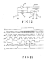
- FIG 12 is a circuit diagram of the oscillation circuit 100.
- Figure 13 is a timing chart illustrating the case where driving pulses P1, P2 for the step motor are varied.
- a quartz oscillator 61 is oscillated by means of an inverter 60, and a gate capacitor 62, a drain capacitor 63, 64 co-operating to enable slight adjustment of the oscillation frequency.
- the capacitors 63, 64 are changed over by a switch 65 in accordance with the control signals Po.
- the control signal Po At the frequency dividing stage, as shown in 0 ⁇ n, 0 ⁇ n + 1 ... in Figure 13 some variation with the control signal Po can be seen. Gradual shortening from the normal cycle tn to ts1 , ts2 and ts3 can be seen with respect to driving pulses P1, P2 for the step motor. Hence, the number of repetitions of driving the step motor increases.
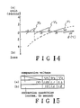
- Figure 14 is a graph showing the effect when discrepancy between indications of the seconds hand is corrected with the compensating circuit of Figure 1.
- Figure 15 is a table of correction showing an example of correction quantities.
- the broken lines in Figure 14 correspond to fluctuations in load which are caused due to the temperature of the viscous rotor, whilst the curved lines correspond to discrepancies between indications of the seconds hand, wherein when setting the time at 25°C, a delay of approximately 4 seconds is present at -10°C, whereas an advance of about 1.4 seconds can be seen at 50°C.
- reference voltages v1, v2, v3 of the detecting unit 110 are individually set to 1.58 V, 1.1 V, 0.6 V respectively, and if the inverse induced voltage changes such as v1 -> v2 -> v3, the driving pulses for the step motor are issued to provide advances equivalent to 1.2 sec, 1.6 sec, 1.8 sec respectively. If the inverse induced voltage varies such as v3 -> v2 -> v1, the correction indicated by the solid line will be effected when the driving pulses are issued to exhibit the corresponding delays.
- Voltages v1, v2, v3 may arbitrarily be set and determined by the resistors 118, 119, 120 ( Figure 8) in the light of the inverse induced voltage levels depicted in Figure 7. In this embodiment, the inverse induced voltages S1, S2 exceed the reference voltage level at 0°C, 20°C and 40°C, and hence correction is also made at these temperatures.
- FIG 16 is a block diagram illustrating another embodiment of a compensating circuit according to the present invention for an electronic watch, the arrangement being such that the compensating circuit is added to a low power consumption driving system of an analog electronic watch known from Japanese Patent Publications Nos. 75520/1979, 77162/1979 and 87977/1977.
- a frequency dividing circuit 106 and a 1/8 up-and-down counter 107 perform the same functions as those in the low power consumption driving system of the conventional analog electronic watch.
- the 1/8 up-and-down counter 107 transmits ⁇ , ⁇ and ⁇ signals in response to the signals from the dividing circuit 106.
- the frequencies of the ⁇ , ⁇ and ⁇ signals are divided from frequency dividing signals 0 ⁇ p corresponding to the driving pulses from the step motor.
- a motor driving pulse/detecting pulse forming circuit 102 applies an optimum pulse width to the coil 1 of the step motor depending on the load.
- a detecting circuit 104 judges whether the step motor rotates or not, and determines the conditions of the ⁇ , ⁇ and ⁇ signals of the 1/8 up-and-down counter 107 in conformity with judgement signals Nr for detecting rotation.
- a pulse number controlling circuit 103 sends control signals Po, Pd in accordance with the driving pulse widths associated with the step motor and also rotation detecting judgement signals from the detecting circuit 104. This varies the driving pulse width depending on the load, and, in turn, the correction quantity is changed in accordance with the variations in the driving pulse width.
- the reference voltage of the detecting circuit 104 may be set at one level which is sufficient to detect rotation and non-rotation of the step motor. Incidentally, there is no problem if circuits for detecting an AC magnetic field and a high frequency magnetic field are added to the detecting circuit, or other methods are applied for changing the pulse width.
- Figure 17 is a graph showing the relation between driving pulse widths P, W and torque T acting on the viscous rotor 14 by means of the step motor. It will be observed that the pulse width is proportional to the torque on the side of W1 having a narrower pulse width, whereas on the side of W8 having a wider pulse width, the torque tends to be saturated.
- Figure 19 is a table of correction, showing one example of the relation between the driving pulse width in driving pulse trains W1 to W8, the values of ⁇ , ⁇ and ⁇ signals of the 1/8 up-and-down counter 107 and the correction quantities.
- the driving pulse width is 1.95 msec, whilst the values of the ⁇ , ⁇ and ⁇ signals are respectively 0, namely, low level.
- the driving pulse width is 2.69 msec, whilst the values of the ⁇ and ⁇ signals are respectively 1, viz., high level, and the ⁇ signal is low level.
- the corresponding quantity indicates an advance when the change is made in the order of W1 -> W2 -> W3.... Whereas in the case of W8 -> W7 -> W6 ..., the correction quantity indicates a delay.
- Figure 18 is a graph showing an example of discrepancy between indications, advance and delay of the seconds hand at a temperature of 0°C.
- the broken lines indicate conditions before the correction is performed, whilst the solid lines indicate the results of correction in another embodiment of a compensating circuit according to the present invention for an electronic watch.
- the step motor is operated with a pulse train W3, i.e. at 2.44 msec, within a range of 10°C to 25°C.
- the pulse width increases with the pulse train W4, i.e. at 2.69 msec.
- the driving pulses are emitted to make an advance equivalent to a correction quantity of 1.1 sec.
- the pulse width becomes 2.44 msec, and the driving pulses are transmitted to make a delay of 1.1 sec.
- the indication returns to its original state, thereby tracing the loci of discrepancies between the indications which are drawn in solid lines.
- the indicational discrepancy is substantially proportional to the load on the viscous rotor owing to the characteristics of the hair spring.
- the characteristics of the step motor do not correspond to the driving pulse widths.
- the correction quantity varies from 1.2 to 0.8 sec.
- the discrepancy between the indications when setting the time at 25°C can be reduced to 1 second at maximum.
- the pulse widths of the pulse trains W7, W8 are required when the load relative to calendar feeding or the like is applied, and the indication delay concomitant with the load can similarly be corrected.
- the present invention aims at correcting the discrepancy between the indications by increasing or decreasing the number of pulses for driving the step motor after detecting the magnitude of the load on the step motor from the inverse induced voltage in the coil of the step motor. Accordingly, there is no limitation to the constitution, the method of detecting the inverse induced current or voltage, the timing and the correcting method or quantity.
- the accumulating means is not limited to the hair spring, but may include other means for accumulating energy, e.g., by storing magnetic force associated with the angular deviation of a pair of magnetic substances disposed relative to each other.
- the controlling means does not involve the exclusive use of a viscous fluid. Even when a load, such as an electro-magnetic brake, undergoes no influence of temperature, and if the foregoing wheel train member imparts fluctuations in load to the actuator (in the illustrated embodiment, the step motor), the discrepancy between the indications associated with variation of load can likewise be corrected.
- the load on the step motor engaging via the wheel train with the hair spring is detected by use of the inverse induced voltage. It is thus possible to correct the discrepancies between the time indications which are concomitant with the variations in viscosity of the viscous fluid of the controlling means and of oil supplied for lubricating the wheel train unit and also with the discontinuous load such as applied during calendar feeding or the like. As a result, the accuracy of the time indication can be considerably increased, thereby attaining an electronic watch with highly accurate sweep hand movement. Thus, the present invention can exhibit tremendous commercial effect.
Landscapes
- Physics & Mathematics (AREA)
- General Physics & Mathematics (AREA)
- Electromechanical Clocks (AREA)
Applications Claiming Priority (2)
| Application Number | Priority Date | Filing Date | Title |
|---|---|---|---|
| JP111020/88 | 1988-05-07 | ||
| JP63111020A JPH01282491A (ja) | 1988-05-07 | 1988-05-07 | 補償回路 |
Related Child Applications (3)
| Application Number | Title | Priority Date | Filing Date |
|---|---|---|---|
| EP94108635.7 Division-Into | 1989-05-04 | ||
| EP94108776.9 Division-Into | 1989-05-04 | ||
| EP94108635 Division | 1989-05-04 |
Publications (2)
| Publication Number | Publication Date |
|---|---|
| EP0342821A2 true EP0342821A2 (de) | 1989-11-23 |
| EP0342821A3 EP0342821A3 (de) | 1991-08-28 |
Family
ID=14550359
Family Applications (1)
| Application Number | Title | Priority Date | Filing Date |
|---|---|---|---|
| EP19890304501 Ceased EP0342821A3 (de) | 1988-05-07 | 1989-05-04 | Kompensationsschaltung für elektronische Uhren |
Country Status (3)
| Country | Link |
|---|---|
| US (1) | US4912689A (de) |
| EP (1) | EP0342821A3 (de) |
| JP (1) | JPH01282491A (de) |
Families Citing this family (3)
| Publication number | Priority date | Publication date | Assignee | Title |
|---|---|---|---|---|
| JP2522912Y2 (ja) * | 1988-12-14 | 1997-01-22 | カシオ計算機株式会社 | ステップモータ駆動回路 |
| JPH02159999A (ja) * | 1988-12-14 | 1990-06-20 | Casio Comput Co Ltd | ステップモータ駆動回路 |
| EP1096640A3 (de) * | 1999-10-25 | 2002-11-27 | Seiko Epson Corporation | Wechselspannungsdetektionsschaltung und -verfahren, Ladeschaltung und -verfahren, Zerhackerschaltung und -verfahren, Zerhackerladeschaltung und -verfahren, elektronische Vorrichtung, und Uhr |
Family Cites Families (12)
| Publication number | Priority date | Publication date | Assignee | Title |
|---|---|---|---|---|
| US2933882A (en) * | 1955-12-30 | 1960-04-26 | Sonobe Shiro | Motor clock provided with a spring automatically wound |
| US3616638A (en) * | 1970-03-19 | 1971-11-02 | Bulova Watch Co Inc | Crystal-controlled mechanical resonator |
| US3978654A (en) * | 1973-06-07 | 1976-09-07 | Kabushiki Kaisha Suwa Seikosha | Motion transformer |
| ES430659A1 (es) * | 1973-10-24 | 1976-11-01 | Jauch | Un procedimiento y un dispositivo para la sincronizacion deun sistema oscilante accionado por un acumulador mecanico deenergia, en especial de un reloj. |
| JPS525566A (en) * | 1975-07-02 | 1977-01-17 | Citizen Watch Co Ltd | Electric clock |
| JPS53132384A (en) * | 1977-04-23 | 1978-11-18 | Seiko Instr & Electronics Ltd | Electronic watch |
| GB2064834B (en) * | 1977-09-26 | 1982-12-08 | Citizen Watch Co Ltd | Drive system for stepping motor in a timepiece |
| JPS5475520A (en) * | 1977-11-30 | 1979-06-16 | Seiko Instr & Electronics Ltd | Operation detecting circuit of step motor |
| JPS5477162A (en) * | 1977-12-02 | 1979-06-20 | Seiko Instr & Electronics Ltd | Electronic watch |
| JPS5587977A (en) * | 1978-12-26 | 1980-07-03 | Seiko Instr & Electronics Ltd | Device for detecting electronic watch |
| JPS5647512A (en) * | 1979-09-26 | 1981-04-30 | Nisshin Steel Co Ltd | Preventing abnormal product produced and deposited in bright annealing furnace |
| CH664868GA3 (de) * | 1986-07-10 | 1988-04-15 |
-
1988
- 1988-05-07 JP JP63111020A patent/JPH01282491A/ja active Pending
-
1989
- 1989-05-04 US US07/347,086 patent/US4912689A/en not_active Expired - Lifetime
- 1989-05-04 EP EP19890304501 patent/EP0342821A3/de not_active Ceased
Also Published As
| Publication number | Publication date |
|---|---|
| EP0342821A3 (de) | 1991-08-28 |
| US4912689A (en) | 1990-03-27 |
| JPH01282491A (ja) | 1989-11-14 |
Similar Documents
| Publication | Publication Date | Title |
|---|---|---|
| US4361410A (en) | Drive system for pulse motor | |
| EP1518319B1 (de) | Vorrichtung und verfahren zum bestimmen der resonanzfrequenz eines oszillationsgerätes, insbesondere einer motorisch angetriebenen zahnbürste | |
| EP0326313B1 (de) | Armbanduhr | |
| EP0695978B1 (de) | Elektronische Kontrolluhr | |
| US5581519A (en) | Analog indicator type electronic timepiece and charging method thereof | |
| US7701807B2 (en) | Analog electronic timepiece that prevents deviation of displayed time when an impact is applied to the timepiece | |
| EP1014227B1 (de) | Zeitmessvorrichtung und verfahren zu ihrer kontrolle | |
| GB2061570A (en) | Electronic timepiece | |
| JP6889220B2 (ja) | 機械式発振器の平均周波数を制御するための電子デバイスと関連付けられた機械式発振器を備える計時器アセンブリ | |
| DE2513845C2 (de) | Elektronische Uhr | |
| EP0342821A2 (de) | Kompensationsschaltung für elektronische Uhren | |
| US4192131A (en) | Step motor control mechanism for electronic timepiece | |
| US4283783A (en) | Drive control system for stepping motor | |
| CN110554595B (zh) | 电子控制式机械钟表、电子控制式机械钟表的控制方法以及电子钟表 | |
| US4479723A (en) | Analog electronic timepiece drive circuitry for energizing stepping motor drive coil in full and intermediate excitation states, and method therefor | |
| US4467256A (en) | Method and device for controlling a stepping motor of a timepiece | |
| CN101090268A (zh) | 一种利用gps定时脉冲调整晶振频率准确度的方法和系统 | |
| GB2082806A (en) | A method of reducing the power consumption of the stepping motor of an electronic timepiece | |
| JP6076344B2 (ja) | 電子時計 | |
| CN1122891C (zh) | 包括用滚筒主弹簧驱动的发电机的一种钟表 | |
| US6630852B2 (en) | Power-generation detection circuit for use in an electronic device and power-generation detection method and power consumption control method for use in connection therewith | |
| HK1002613B (en) | Method for feeding a monophase stepping motor | |
| US4590412A (en) | Method of energizing a stepping motor | |
| CN1038358A (zh) | 电子表 | |
| US6737834B2 (en) | Engine control apparatus with an alternator regulator circuit interface means, and a corresponding interface |
Legal Events
| Date | Code | Title | Description |
|---|---|---|---|
| PUAI | Public reference made under article 153(3) epc to a published international application that has entered the european phase |
Free format text: ORIGINAL CODE: 0009012 |
|
| AK | Designated contracting states |
Kind code of ref document: A2 Designated state(s): CH FR GB LI |
|
| PUAL | Search report despatched |
Free format text: ORIGINAL CODE: 0009013 |
|
| AK | Designated contracting states |
Kind code of ref document: A3 Designated state(s): CH FR GB LI |
|
| 17P | Request for examination filed |
Effective date: 19920131 |
|
| 17Q | First examination report despatched |
Effective date: 19921214 |
|
| STAA | Information on the status of an ep patent application or granted ep patent |
Free format text: STATUS: THE APPLICATION HAS BEEN REFUSED |
|
| 18R | Application refused |
Effective date: 19951002 |