EP0342656A2 - Herstellung einer aus einem Verbindungshalbleiter bestehenden lichtemittierenden Vorrichtung - Google Patents
Herstellung einer aus einem Verbindungshalbleiter bestehenden lichtemittierenden Vorrichtung Download PDFInfo
- Publication number
- EP0342656A2 EP0342656A2 EP89108888A EP89108888A EP0342656A2 EP 0342656 A2 EP0342656 A2 EP 0342656A2 EP 89108888 A EP89108888 A EP 89108888A EP 89108888 A EP89108888 A EP 89108888A EP 0342656 A2 EP0342656 A2 EP 0342656A2
- Authority
- EP
- European Patent Office
- Prior art keywords
- light emitting
- compound semiconductor
- emitting device
- substrate
- manufacturing
- Prior art date
- Legal status (The legal status is an assumption and is not a legal conclusion. Google has not performed a legal analysis and makes no representation as to the accuracy of the status listed.)
- Granted
Links
Images

Classifications
-
- H—ELECTRICITY
- H10—SEMICONDUCTOR DEVICES; ELECTRIC SOLID-STATE DEVICES NOT OTHERWISE PROVIDED FOR
- H10H—INORGANIC LIGHT-EMITTING SEMICONDUCTOR DEVICES HAVING POTENTIAL BARRIERS
- H10H20/00—Individual inorganic light-emitting semiconductor devices having potential barriers, e.g. light-emitting diodes [LED]
- H10H20/01—Manufacture or treatment
- H10H20/011—Manufacture or treatment of bodies, e.g. forming semiconductor layers
- H10H20/013—Manufacture or treatment of bodies, e.g. forming semiconductor layers having light-emitting regions comprising only Group III-V materials
-
- C—CHEMISTRY; METALLURGY
- C30—CRYSTAL GROWTH
- C30B—SINGLE-CRYSTAL GROWTH; UNIDIRECTIONAL SOLIDIFICATION OF EUTECTIC MATERIAL OR UNIDIRECTIONAL DEMIXING OF EUTECTOID MATERIAL; REFINING BY ZONE-MELTING OF MATERIAL; PRODUCTION OF A HOMOGENEOUS POLYCRYSTALLINE MATERIAL WITH DEFINED STRUCTURE; SINGLE CRYSTALS OR HOMOGENEOUS POLYCRYSTALLINE MATERIAL WITH DEFINED STRUCTURE; AFTER-TREATMENT OF SINGLE CRYSTALS OR A HOMOGENEOUS POLYCRYSTALLINE MATERIAL WITH DEFINED STRUCTURE; APPARATUS THEREFOR
- C30B25/00—Single-crystal growth by chemical reaction of reactive gases, e.g. chemical vapour-deposition growth
- C30B25/02—Epitaxial-layer growth
-
- H—ELECTRICITY
- H01—ELECTRIC ELEMENTS
- H01S—DEVICES USING THE PROCESS OF LIGHT AMPLIFICATION BY STIMULATED EMISSION OF RADIATION [LASER] TO AMPLIFY OR GENERATE LIGHT; DEVICES USING STIMULATED EMISSION OF ELECTROMAGNETIC RADIATION IN WAVE RANGES OTHER THAN OPTICAL
- H01S5/00—Semiconductor lasers
- H01S5/30—Structure or shape of the active region; Materials used for the active region
- H01S5/32—Structure or shape of the active region; Materials used for the active region comprising PN junctions, e.g. hetero- or double- heterostructures
- H01S5/323—Structure or shape of the active region; Materials used for the active region comprising PN junctions, e.g. hetero- or double- heterostructures in AIIIBV compounds, e.g. AlGaAs-laser, InP-based laser
- H01S5/32308—Structure or shape of the active region; Materials used for the active region comprising PN junctions, e.g. hetero- or double- heterostructures in AIIIBV compounds, e.g. AlGaAs-laser, InP-based laser emitting light at a wavelength less than 900 nm
- H01S5/32325—Structure or shape of the active region; Materials used for the active region comprising PN junctions, e.g. hetero- or double- heterostructures in AIIIBV compounds, e.g. AlGaAs-laser, InP-based laser emitting light at a wavelength less than 900 nm red laser based on InGaP
Definitions
- This invention relates to a light emitting device including a compound semiconductor, and more particularly to a light emitting device of a III-V compound semiconductor having uniform and high light emitting intensity, such as a semiconductor laser in particular, and a method of manufacturing such a light emitting device.
- III-V compound semiconductors are utilized as the material of optoelectronic devices for converting an electrical input into an optical output by applying a forward-bias to the pn junction of the semiconductor, e.g., a semiconductor laser adapted to take out a stimulated emission light produced by recombination of the carrier, or a light emitting diode adapted to take out a spontaneous emission light produced by recombination of the carrier.
- a forward-bias to the pn junction of the semiconductor, e.g., a semiconductor laser adapted to take out a stimulated emission light produced by recombination of the carrier, or a light emitting diode adapted to take out a spontaneous emission light produced by recombination of the carrier.
- semiconductor lasers are small, light, and are easy to handle, attention is focused thereupon as a light source used for information equipment such as video disks, measurement equipment, optical communication equipment, and the like in place of the He-Ne lasers which have been conventionally used.
- a great interest in particularly short wavelength semiconductor lasers is taken from the viewpoint of improvements in the performance of the system.
- III-V compound semiconductors for the material capable of oscillating at a short wavelength of about 600 nm band and less, there are III-V compound semiconductors, and especially AlGaInP mixed crystal is particular.
- the manufacturing process of the III-V compound semiconductor is as follows. First, organic metal compound including the group III devices and hydride compound of group V devices constituting the III-V compound semiconductor, are transported onto a substrate under a high temperature condition. They are caused to react and undergo crystal growth on the substrate by the metal organic chemical vapor deposition (MOCVD) method in addition to MBE (molecular beam epitaxy) method. Thus, the III-V compound semiconductor is obtained as a crystal film. However, satisfactory crystals could not necessarily be obtained and control of the composition was difficult.
- MOCVD metal organic chemical vapor deposition
- the oscillation wavelength can be equal to a short wavelength of about 600 nm, but the oscillation intensity to be maintained at a high level is lowered.
- the quantity of material gas used necessary per each compound semiconductor is increased, resulting in increased manufacturing cost.
- a large quantity of used material gas, i.e., exhaust gas may be produced, large investment and/or troublesome operation are required for treatment of the exhaust gas which is poisonous.
- This invention has been made under the above-described background, and its object is to provide a AlGaInP light emitting device having an oscillation wavelength in the short wavelength of 600 nm band and having a sufficient oscillation intensity, and to provide a method of manufacturing such a light emitting device, thereby making it possible to reduce the quantity of material gas used, and to lessen the burden on exhaust gas treatment.
- a compound semiconductor light emitting device of this invention includes an active layer of a monocrystalline thin film comprised of a compound semiconductor expressed as the equation (Al z Ga 1-z ) x In 1-x P (x is a number where lattice-matching on the GaAs substrate can be realized, e.g., a number within a range from 0.48 to 0.55, and z is a number within a range from 0.08 to 0.25, preferably a number within a range from 0.18 to 0.25), and has an oscillating wavelength at least in the 606 nm band.
- a method of manufacturing a compound semiconductor light emitting device is directed to a method of forming AlGaInP compound semiconductor crystal film on a substrate, to therefore manufacture a compound semiconductor light emitting device, the method including the steps of: transporting a material gaseous phase mixture constituting of an organic metal compound including a group III device and hydride of phosphorus constituting the compound semiconductor into a lateral type reactive tube adapted to allow material gas to flow in a horizontal direction at a feed rate of less than 30 cm/sec, preferably 18 to 23 cm/sec and a gas pressure of less than 60 Torr, preferably within a range from 45 to 55 Torr, mounting thereon a substrate for growing a compound semiconductor crystal on a substrate table within the lateral type reactive tube so that the substrate surface forms an angle of 3 to 45°, preferably, 3 to 10° relative to the horizontal direction to rotate the substrate table about the axis in a direction perpendicular to the substrate surface, and growing on the substrate a monocrystalline thin film of a compound semiconductor expressed as the equation
- group V material gas is at a transported low concentration into the reactive tube under conditions of slow feed flow rate and low gas pressure, the quantity of material used may be reduced. Thus, the manufacturing cost is reduced and the troublesomeness of the exhaust gas treatment is lessened.
- the semiconductor light emitting device has an oscillating wavelength in the 600 nm band, particularly at least in the short wavelength of 606 nm.
- the method of manufacturing a compound semiconductor according to this invention is directed to a method of forming an AlGaInP compound semiconductor crystal film on a substrate under the conditions of specified material feed and the crystal growth, to therefore manufacture a compound semiconductor light emitting device.
- organic metal compounds including group III devices and hydrides of phosphorous constituting the AlGaInP compound semiconductor of the final object.
- organic metal compound containing aluminum there is alkyl aluminum such as triethyl aluminum, trimethyl aluminum, or ethylmethyl aluminum.
- organic metal compound containing gallium there is alkyl gallium such as triethyl gallium, trimethyl gallium, or ethylmethyl gallium.
- organic metal compound containing indium there is alkyl indium such as triethyl indium, trimethyl indium, or ethylmethyl indium.
- phosphine there is phosphine.
- the feed of material in this invention is conducted in a manner whereby material in the form of a gaseous phase mixture is transported into the lateral type reactive tube at a feed flow rate of less than 30 cm/sec, preferably 18 to 23 cm/sec, and at a pressure within the tube of less than 60 Torr, preferably 45 to 55 Torr.
- the substrate on which a target crystal film is formed may be GaAs substrate of (100) plane set at a predetermined temperature, GaAs substrate of (100) plane having various epitaxial grown layers formed on the substrate surface, or the like, and its form or configuration and dimension may be arbitrarily determined.
- a manufacturing apparatus used in the manufacturing method of this invention is provided with a lateral type reactive tube through which material mixed gas flows in a state considered as a laminar flow in a horizontal direction as since the lateral type reactive tube is used in this invention, there is no possibility that the reactive gas heated in the vicinity of the place where the substrate is provided may be circulated by convection upwardly and downwardly as in the vertical type reactive tube, therefore making it possible to uniformly grow a crystal of the compound semiconductor on the substrate surface.
- the material mixed gas admitted into the lateral type reactive tube is transported under the conditions of the flow rate and pressure described above.
- the substrate surface on which the crystal film is grown is inclined so as to have an angle of 3 to 45°, preferably 3 to 10° relative to the direction of flow of the material mixed gas, i.e., substantially horizontal direction.
- This may be implemented by mounting the substrate table (graphite susceptor) for mounting the substrate thereon in a manner as stated above.
- an employment of the device so that the substrate surface is inclined can overcome the inconveniences encountered with the case where the substrate is horizontally mounted, namely that the crystal growth rate is considerably slow, and that a large quantity of poisonous gas is produced.
- the substrate surface on which the crystal is to be grown is rotated about the axis in a direction perpendicular to the substrate surface. Such a rotation may be conducted by rotating the substrate table on which the substrate is mounted. By rotating the substrate surface in this way, the growth generation conditions upstream of the gas flow on the substrate surface and that downstream thereof can be equalized. Thus, a compound semiconductor having a uniform composition characteristic can be provided.
- manufacturing parameters such as the temperature may be suitably selected and altered according to purposes.
- FIG. 1 is a side cross sectional view showing the principal part of an example of the lateral type reactive tube which can be used in the manufacturing method of this invention.
- the material mixed gas flows in a state considered as a laminar flow in a horizontal direction within the reactive tube.
- a substrate table 2 is rotatably provided.
- a substrate 3 on which a compound semiconductor crystal film is to be grown is mounted on the upper surface 2a of the substrate table 2.
- the substrate table 2 is of a structure such that it can have an angle ⁇ of 3 to 45° relative to the flowing direction of the material mxied gas, i.e., the horizontal direction, and is supported by a supporting shaft 5 inserted into a recess 2c.
- a conduit 1a for the material gas is formed on the upstream side of the lateral type reactive tube 1, and an exhaust hole 1b for an exhaust gas is formed on the downstream side.
- an exhaust pipe 6 is fitted into the exhaust hole 1b.
- a rotary shaft 4 is rotatably affixed.
- a toothed wheel 7 is provided on the end portion on the side of the substrate table of the rotary shaft 4. This toothed wheel 7 meshes with a toothed portion 2b provided along the outer circumferential surface of the substrate table 2. Thus, it becomes operative in cooperation with the substrate table 2.
- the rotary shaft 4 is connected to a rotational drive surface (not shown) such as a motor.
- material mixed gas adjusted so as to have a predetermined mixing ratio is introduced from the conduit 1a into the lateral reactive tube 1 at a predetermined flow rate.
- the mixed gas thus introduced flows in a horizontal direction forming a steady laminar flow.
- the rotary shaft 4 connected to a motor (not shown) provided outside the exhaust pipe transmits the rotational drive force to the toothed wheel 7.
- the substrate table 2 inclined at an angle ⁇ and the substrate 3 mounted on the upper surface 2a of the substrate table rotates about the shaft (the supporting shaft 5) in a direction perpendicular to the substrate surface.
- the rotational speed of the substrate is arbitrary in this invention, it is preferable that the rotational speed is ordinarily set to less than 3 rpm in order to allow the compound semiconductor thus obtained to have an excellent performance.
- the semiconductor light emitting device of this invention includes an active layer of a monocrystalline thin film comprised of a compound semiconductor expressed as the equation (Al z Ga 1-z ) x In 1-x P (x is a number where lattice-matching on the GaAs substrate can be realized, e.g., a number within a range from 0.48 to 0.55, and z is a number within a range from 0.08 to 0.25, preferably a number within a range from 0.18 to 0.25), and has an oscillating wavelength at least in the 606 nm band.
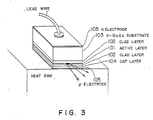
- FIG. 3 An example of the structure of a compound semiconductor laser according to this invention is shown in FIG. 3.
- the active layer 101 and the clad layer 102 which have been made to form a double hetero junction are epitaxially grown on the GaAs substrate 103.
- the clad layer 102 serves to confine carriers and photons in the active layer 101.
- the cap layer 104 is provided for reducing the contact resistance with the electrode portion 105.
- the pn junction is provided at the boundary between the active layer 101 and the clad layer 102.
- the light emitting device of this invention is not limited to the embodiment shown and may be implemented in various manners.
- an AlGaInP compound semiconductor crystal film is formed on the substrate using the manufacturing apparatus provided with a lateral reactive tube of the structure shown in FIG. 1, to therefore manufacture a compound semiconductor light emitting device.
- a quartz glass tube having an inner diameter of 100 mm and a length of 650 mm was used as the reactive tube body, and carbon material (high purity carbon and SiC coated carbon) was used as the material of the substrate table (graphite susceptor).
- a GaAs substrate having an area of 1 cm2 as the substrate was mounted on the substrate table.
- the substrate surface was (100) planar.
- the substrate table was inclined so that the substrate surface formed an angle of 5° relative to the horizontal direction of the material gas flow.
- the substrate table and the substrate mounted thereon were rotated about the supporting shaft.
- the rotational speed was 2/3 to 1 rpm.
- the pressure within the reactive tube was set to 50 torr and the growth temperature (substrate temperature) of the compound semiconductor was set to 715 ⁇ 10°C.
- organic metal compound including the group III device trimethyl aluminum, trimethyl gallium and trimethyl indium were used.
- phosphine was used for hydride of phosphorous.
- the compound semiconductor crystal film thus obtained was 1.0 ⁇ m (micron) in the film thickness, and the surface of the grown layer was spherical.
- the light emitting intensity of the compound semiconductor crystal film thus obtained was evaluated.
- the clad layer was further formed on the substrate on which the compound semiconductor film of the active layer was formed by the ordinary technique, to therefore prepare a semiconductor laser.
- the semiconductor laser thus prepared had an oscillating wavelength at least in the 606 nm band.
- the light emitting intensity of the compound semiconductor crystal film thus obtained was evaluated, to therefore prepare a semiconductor laser.
- the semiconductor laser thus prepared has an oscillating wavelength at least in the 606 nm band.
- the light emitting intensity of the compound semiconductor crystal film thus obtained was evaluated, to therefore prepare a semiconductor laser.
- the semiconductor laser thus prepared has an oscillating wavelength at least in the 606 nm band.
- the light emitting intensity of the compound semiconductor crystal film thus obtained was evaluated, to therefore prepare a semiconductor laser.
- the semiconductor laser thus prepared has an oscillating wavelength at least in the 606 nm band.
Landscapes
- Chemical & Material Sciences (AREA)
- Physics & Mathematics (AREA)
- Chemical Kinetics & Catalysis (AREA)
- Electromagnetism (AREA)
- Optics & Photonics (AREA)
- General Physics & Mathematics (AREA)
- Condensed Matter Physics & Semiconductors (AREA)
- General Chemical & Material Sciences (AREA)
- Engineering & Computer Science (AREA)
- Crystallography & Structural Chemistry (AREA)
- Materials Engineering (AREA)
- Metallurgy (AREA)
- Organic Chemistry (AREA)
- Semiconductor Lasers (AREA)
Applications Claiming Priority (4)
| Application Number | Priority Date | Filing Date | Title |
|---|---|---|---|
| JP11814688 | 1988-05-17 | ||
| JP118146/88 | 1988-05-17 | ||
| JP166698/88 | 1988-07-06 | ||
| JP16669888 | 1988-07-06 |
Publications (3)
| Publication Number | Publication Date |
|---|---|
| EP0342656A2 true EP0342656A2 (de) | 1989-11-23 |
| EP0342656A3 EP0342656A3 (en) | 1990-03-28 |
| EP0342656B1 EP0342656B1 (de) | 1994-01-19 |
Family
ID=26456131
Family Applications (1)
| Application Number | Title | Priority Date | Filing Date |
|---|---|---|---|
| EP89108888A Expired - Lifetime EP0342656B1 (de) | 1988-05-17 | 1989-05-17 | Herstellung einer aus einem Verbindungshalbleiter bestehenden lichtemittierenden Vorrichtung |
Country Status (4)
| Country | Link |
|---|---|
| EP (1) | EP0342656B1 (de) |
| KR (1) | KR900019140A (de) |
| CA (1) | CA1313247C (de) |
| DE (1) | DE68912398D1 (de) |
Cited By (4)
| Publication number | Priority date | Publication date | Assignee | Title |
|---|---|---|---|---|
| EP0434233A1 (de) * | 1989-12-18 | 1991-06-26 | Hewlett-Packard Company | Lichtemittierende Diode mit einer elektrisch leitenden Fensterschicht |
| EP0487822A1 (de) * | 1990-11-27 | 1992-06-03 | Pioneer Electronic Corporation | Lichtaussendes Halbleiterelement |
| US20180057938A1 (en) * | 2016-08-29 | 2018-03-01 | Nuflare Technology, Inc. | Vapor-phase growth method |
| CN113612108A (zh) * | 2021-08-03 | 2021-11-05 | 上海交通大学 | 一种基于斜切非线性晶体脊型波导的频率转换器及其制备方法 |
-
1989
- 1989-05-16 CA CA000599861A patent/CA1313247C/en not_active Expired - Fee Related
- 1989-05-17 EP EP89108888A patent/EP0342656B1/de not_active Expired - Lifetime
- 1989-05-17 DE DE89108888T patent/DE68912398D1/de not_active Expired - Lifetime
- 1989-05-17 KR KR1019890006580A patent/KR900019140A/ko not_active Withdrawn
Cited By (5)
| Publication number | Priority date | Publication date | Assignee | Title |
|---|---|---|---|---|
| EP0434233A1 (de) * | 1989-12-18 | 1991-06-26 | Hewlett-Packard Company | Lichtemittierende Diode mit einer elektrisch leitenden Fensterschicht |
| EP0487822A1 (de) * | 1990-11-27 | 1992-06-03 | Pioneer Electronic Corporation | Lichtaussendes Halbleiterelement |
| US5274251A (en) * | 1990-11-27 | 1993-12-28 | Pioneer Electronic Corporation | Semiconductor light emitting element |
| US20180057938A1 (en) * | 2016-08-29 | 2018-03-01 | Nuflare Technology, Inc. | Vapor-phase growth method |
| CN113612108A (zh) * | 2021-08-03 | 2021-11-05 | 上海交通大学 | 一种基于斜切非线性晶体脊型波导的频率转换器及其制备方法 |
Also Published As
| Publication number | Publication date |
|---|---|
| DE68912398D1 (de) | 1994-03-03 |
| EP0342656A3 (en) | 1990-03-28 |
| EP0342656B1 (de) | 1994-01-19 |
| CA1313247C (en) | 1993-01-26 |
| KR900019140A (ko) | 1990-12-24 |
Similar Documents
| Publication | Publication Date | Title |
|---|---|---|
| KR100484482B1 (ko) | 질화갈륨결정에의 산소도핑방법과 산소도핑된 질화갈륨단결정기판 | |
| EP0523917A2 (de) | Atomschicht-Epitaxie-Aufwachsen von Verbindungshalbleiter | |
| US5442201A (en) | Semiconductor light emitting device with nitrogen doping | |
| EP0524817B1 (de) | Verfahren zur Kristallzüchtung eines III-V Verbindungshalbleiters | |
| JP3143040B2 (ja) | エピタキシャルウエハおよびその製造方法 | |
| EP0342656B1 (de) | Herstellung einer aus einem Verbindungshalbleiter bestehenden lichtemittierenden Vorrichtung | |
| US5015327A (en) | Method for producing semiconductive single crystal | |
| JP3399642B2 (ja) | 半導体発光素子層の形成方法 | |
| US4983249A (en) | Method for producing semiconductive single crystal | |
| US5622559A (en) | Method of preparing compound semiconductor | |
| KR960004591B1 (ko) | 도우프된 결정 성장 방법 | |
| JP2754549B2 (ja) | Ga▲下0▼.▲下5▼In▲下0▼.▲下5▼P結晶の成長方法 | |
| JP2946280B2 (ja) | 半導体結晶成長方法 | |
| JP2519232B2 (ja) | 化合物半導体結晶層の製造方法 | |
| JPH02125485A (ja) | 化合物半導体発光素子 | |
| JP2590728B2 (ja) | 化合物半導体の選択成長方法 | |
| US6245144B1 (en) | Doping control in selective area growth (SAG) of InP epitaxy in the fabrication of solid state semiconductor lasers | |
| JP3052399B2 (ja) | 化合物半導体膜の製造方法 | |
| JPH0620042B2 (ja) | ▲iii▼−▲v▼族化合物半導体結晶のド−ピング方法 | |
| JPS6265996A (ja) | 化合物半導体結晶層の製造方法 | |
| EP0504960A1 (de) | Filme aus phosphorlegiertem, kubischem Bornitrid | |
| JPS6134987A (ja) | 半導体レ−ザの製造方法 | |
| JPH0682864B2 (ja) | 半導体発光素子とその製造方法 | |
| JPH0652718B2 (ja) | ド−ピング方法 | |
| JPH01320297A (ja) | 化合物半導体薄膜の成長方法 |
Legal Events
| Date | Code | Title | Description |
|---|---|---|---|
| PUAI | Public reference made under article 153(3) epc to a published international application that has entered the european phase |
Free format text: ORIGINAL CODE: 0009012 |
|
| AK | Designated contracting states |
Kind code of ref document: A2 Designated state(s): DE FR GB NL |
|
| PUAL | Search report despatched |
Free format text: ORIGINAL CODE: 0009013 |
|
| AK | Designated contracting states |
Kind code of ref document: A3 Designated state(s): DE FR GB NL |
|
| 17P | Request for examination filed |
Effective date: 19900511 |
|
| 17Q | First examination report despatched |
Effective date: 19920727 |
|
| GRAA | (expected) grant |
Free format text: ORIGINAL CODE: 0009210 |
|
| AK | Designated contracting states |
Kind code of ref document: B1 Designated state(s): DE FR GB NL |
|
| PG25 | Lapsed in a contracting state [announced via postgrant information from national office to epo] |
Ref country code: FR Effective date: 19940119 Ref country code: DE Effective date: 19940119 |
|
| REF | Corresponds to: |
Ref document number: 68912398 Country of ref document: DE Date of ref document: 19940303 |
|
| PG25 | Lapsed in a contracting state [announced via postgrant information from national office to epo] |
Ref country code: GB Effective date: 19940517 |
|
| EN | Fr: translation not filed | ||
| PLBE | No opposition filed within time limit |
Free format text: ORIGINAL CODE: 0009261 |
|
| STAA | Information on the status of an ep patent application or granted ep patent |
Free format text: STATUS: NO OPPOSITION FILED WITHIN TIME LIMIT |
|
| PG25 | Lapsed in a contracting state [announced via postgrant information from national office to epo] |
Ref country code: NL Effective date: 19941201 |
|
| 26N | No opposition filed | ||
| GBPC | Gb: european patent ceased through non-payment of renewal fee |
Effective date: 19940517 |
|
| NLV4 | Nl: lapsed or anulled due to non-payment of the annual fee |