EP0341897B1 - Content addressable memory array architecture - Google Patents
Content addressable memory array architecture Download PDFInfo
- Publication number
- EP0341897B1 EP0341897B1 EP89304467A EP89304467A EP0341897B1 EP 0341897 B1 EP0341897 B1 EP 0341897B1 EP 89304467 A EP89304467 A EP 89304467A EP 89304467 A EP89304467 A EP 89304467A EP 0341897 B1 EP0341897 B1 EP 0341897B1
- Authority
- EP
- European Patent Office
- Prior art keywords
- match
- array
- bit
- bits
- data
- Prior art date
- Legal status (The legal status is an assumption and is not a legal conclusion. Google has not performed a legal analysis and makes no representation as to the accuracy of the status listed.)
- Expired - Lifetime
Links
Images


Classifications
-
- G—PHYSICS
- G11—INFORMATION STORAGE
- G11C—STATIC STORES
- G11C15/00—Digital stores in which information comprising one or more characteristic parts is written into the store and in which information is read-out by searching for one or more of these characteristic parts, i.e. associative or content-addressed stores
- G11C15/04—Digital stores in which information comprising one or more characteristic parts is written into the store and in which information is read-out by searching for one or more of these characteristic parts, i.e. associative or content-addressed stores using semiconductor elements
-
- G—PHYSICS
- G06—COMPUTING OR CALCULATING; COUNTING
- G06F—ELECTRIC DIGITAL DATA PROCESSING
- G06F16/00—Information retrieval; Database structures therefor; File system structures therefor
- G06F16/90—Details of database functions independent of the retrieved data types
- G06F16/903—Querying
- G06F16/90335—Query processing
- G06F16/90339—Query processing by using parallel associative memories or content-addressable memories
Definitions
- This application relates to systems employing content addressable memory (CAM) arrays in which a memory is searched on the basis of the contents of the memory data rather than by the data location in the memory.
- CAM content addressable memory
- CAM content addressable memory
- the array includes a plurality of word lines (ROW SELECT) and match lines (ROW MATCH) extending in a first direction and bit line pairs (DATA,DATA) extending in a second direction perpendicular to the first direction.
- ROW SELECT word lines
- ROW MATCH match lines
- DATA,DATA bit line pairs
- Content-addressable memory a storage device that stores data in a number of cells. The cells can be accessed or loaded on the basis of their contents.
- Content-addressable processor a content-addressable memory in which more sophisticated data transformations can be performed on the contents of a number of cells selected according to the contents, or a computer or computer system that uses such memory as an essential component for storage or processing, respectively.
- Accessing data on the basis of their content always involves some comparison of an external search argument with part or all of the information stored in all cells. Whether this is done by software, mechanical scanning or parallel electronic circuits, is immaterial in principle; however, a "genuine" content-addressable memory performs all comparisons in parallel. Another fact to emphasize is that comparison by equality match between the search argument and the stored item is not the only mode used. If the stored data have numerical values, the purpose of content-addressable search may be to locate all cells the contents of which satisfy certain magnitude relations with respect to the search arguments; for instance, between greater than or less than the given limit, or between two specified limits. Content-addressable searching is sometimes performed without reference to an external search argument, for instance, when locating the maximum or minimum in a set of stored numbers.
- Hardware content-addressable memories have been used as special parts in computing systems, in certain organizational solutions whereby the CAMs can effectively perform fast buffering, checking, and bookkeeping operations needed in the moving and rearrangement of data. In this way the CAM devices can effectively contribute to the speed of usual operations by making the operands more directly available to the processing circuits.
- a masked search in a CAM array only a subset of the bits of a search-argument word is compared with respective bits of all memory words.
- Masking in the CAM usually means masking out, or disablement of certain bits. Those stored words which agree in the specified (unmasked) bit positions with the search argument are then read out.
- a CAM array package having a configuration with N bit wide words and M words deep for example, 48 bit words, with 256 words in the array
- N bit wide words and M words deep for example, 48 bit words, with 256 words in the array
- the following pin count would be needed for a typical nonmultiplexed 256 by 48 CAM array using prior art techniques.
- a content addressable memory system according to the present invention is defined in claim 1.
- the arrangement employs three 48 bit internal registers to hold the CAM data, the unmasked match word and the mask bits. These three 48 bit registers can be loaded in three cycles from the 16 bit I/O bus.
- a command write cycle and a status read cycle are utilized in this arrangement to further multiplex the address, instructions and flag information to and from the 16 bit bus. This latter is done at the expense of an extra control signal(D/ C ⁇ -Data/Command).
- the write command takes on the format of a command word, with operational (OP) codes encoded in some of the word bits and addresses information encoded in others of the bits.
- OP operational
- information as to flag status is encoded in part of the status word bits and address information is encoded in other of the status word bits.
- the required pin count is reduced to the following: I/O 16 pins Control Signals 4 pins Flags (Match; full) 2 pins Power supplies (fewer Vcc and Vss pairs are required for the output) 6 pins Total 28 pins
- a CAM array in which any or all of the bits in a word can be maskable and any or all of the words in the array can be both maskable and resettable.
- a further feature of this arrangement is the particular CAM processor architecture employed. This architecture involves the following structure:
- the CAM cell array 11 of the present invention is organized in N-bit wide words and M words deep.
- a typical, but not limiting, example comprises an array of 48 bit words, with 256 such words in the array. Two extra bits (skip bit and empty bit) are attached to each word for word masking and reset purposes.
- a bit line descriptor circuit 1 (shown in more detail in Fig. 2) which includes a programmable bit line writing circuit, a comparand register, a mask register, and a sense amplifier. Descriptor circuitry 1 exchanges data with a 16 bit bus 10.
- a row decoder 2 is connected to array 11 through a bus containing a plurality of word lines WL for selecting different words in the array.
- a bit-line precharge circuit 3 is connected to array 11 through a plurality of bit lines BL and BL, a pair of such bit lines being provided for each column of bits in the array.
- Communicating with the output of array 11 through match lines ML are a word masking and reset circuit 4, a match detector 5 and a priority encoder 6.
- a control logic network 7 provides inputs to circuits 4, 5 and 6 in response to instructions received from bus 10. Circuits 4, 5 and 6 communicate directly with bus 10, the communication between bus 10 and circuit 4 being bidirectional. The details of these circuits are shown in more detail in Fig. 2.
- bit-line descriptor circuitry 1 from Fig. 1 are shown in the dotted enclosure 1 and include a CAM register 17, a mask register 18, a compound register 19, a sense amplifier 14 and a programmable bit line writing circuit included in a descriptor element 36.
- the circuit of Fig. 2 also shows an address decoder 30 corresponding in function to row decoder 2 of Fig. 1 to decode the eight address bits supplied from bus 10 to identify the one of the 256 words in array 11 to be selected. Also shown connected to the output of array 11 and to decoder 30 are a skip bit array 22 having a skip write circuit 20, and an empty bit array 24 having an empty write circuit 23. Outputs from elements 22 and 24 are supplied to skip/empty bits element 41.
- a full detector 31 controlled by a full control element 37 and supplying an output to a status register 40 and to a full register 32.
- Status register 40 communicates in a 16 bit manner with bus 10 during a status read operation.
- a match detector 28 controlled by a match control element 38 supplies a single match signal to a match register 29. Signals from full register 32 and match register 29 are supplied to full flag element 26 and match flag element 27, respectively. Match detector 28 also supplies both the single match signal and a multiple match signal to status register 40.
- Fig. 2 also shows a priority multiplexor 25 which multiplexes the information from elements 28 and 31 to a priority encoder under the control of a multiplexor control element 33.
- a segment counter 34 is under the control of a counter control element 35 which is connected to bus 10 and to the output of OP code generator 39. Counter 34 supplies one input to status register 40 and another output to an output field selector and data read element 42.
- the system of the present invention has four modes of operation, which are command write (CW), data write (DW), status read (SR), and data read (DR), as shown by the corresponding blocks on the output of a mode generator 13 in Fig. 2.
- data write mode data is written into the comparand register.
- Mode generator 13 receives a chip enable signal on a pin E ⁇ , an output enable signal on a pin G ⁇ , a write enable signal on a pin W ⁇ , and a command/data signal on a pin D/ C ⁇ .
- Comparand register 19 is the main buffer between bus 10 and CAM array 11. After a data write operation is performed, one of the operation (OP) codes is carried out under the control of the command write cycle to move data into CAM array 11 or mask register 17.
- the command write instruction is encoded on the 16 bit bus 10.
- 16 bits on bus 10 4 bits are used to decode the 16 OP codes employed in the present invention.
- the OP codes employed in the present invention are listed below.
- Op Code 0 Initialization All Skip-bits are set to LOW (don't skip) and all Empty-bits are set to HIGH (empty).
- the /MTCH and /FULL outputs are enabled.
- the mode is set to 48-bit mode.
- the Mask register and Segment counter are reset to zero. By default, subsequent data writes and reads are to and from the comparand register.
- Op Code 1 Output control Match and full flags are enabled or disabled by this command.
- Op Code 2 Mode select User can use this command to select between 16 or 48 bit mode. In 16-bit mode, the Segment counter is never incremented.
- Op Code 3 Move Comparand Register to Mask Register Contents of the Comparand register data is moved into the Mask register.
- Op Code 4 Move Mask Register to Comparand Register Contents of the Mask register data is moved into the comparand register.
- Op Code 5 Enable Output from Skip and Empty Bit Array to I/O port All subsequent data mode reads result in data flowing from Empty-bits and Skip-bits to the output buffer. Address is specified by the command register address field.
- Op Code 6 Move Comparand Register to CAM Contents of the Comparand register data is moved into the CAM.
- the Empty-bit and Skip-bit are not changed.
- the CAM address is specified by the command word address field.
- the Segment counter is not changed.
- Op Code 7 Move CAM to Comparand Register Contents of the CAM data specified by the command word address field is moved into the Comparand register.
- the Segment counter is not changed.
- the Skip and Empty Bit Array information is not changed.
- Op Code 9 Skip-bit control User can write to Skip-bit array using this command. They can write the whole array in one cycle or any individual bit by providing the desired address location.
- Op Code 10 Empty-bit control User can write to Empty-bit array using this command. They can write the whole array in one cycle or any individual bit by providing the desired address location.
- Op Code 11 Enable Output from Comparand Register to I/O Port All subsequent data reads result in data flowing from the Comparand register segment to the output buffer.
- Op Code 12 Enable Output from Mask Register to I/O port All subsequent data reads result in data flowing from the Mask register segment to the output buffer.
- Op Code 13 Enable Output from CAM to I/O port All subsequent data reads result in data flowing from the CAM segment to the output buffer.
- CAM address is specified by the command word address field.
- Op Code 14 Move Ccmparand Register to CAM (Reset Empty bit and Skip bit both LOW) Contents of the comparand register data is moved into address specified by the command word address field (CAM address). The corresponding Empty bit and Skip bit are both reset to LOW.
- Op Code 15 Load Segment Counter User can change the segment counter to get to any one of the 3 segments.
- a status read is normally an operation following a match operation where the user wants to know the match location, whether it's a multiple or single match, and if the chip is still full.
- the contents of status register 40 can be read out onto bus 10. Two bits can be read from segment counter 22, eight bits from the address position indication from priority encoder 21 and three flag bits from full detector 31 and from the match and multiple match detector 28.
- the status word employed in the present invention can be described as follows: As shown below, the lower eight bit of the status word are the encoded address to indicate to the user the location.
- the upper three bits identify the status flags, including a multiple match flag, a full flag and a match flag. These internal flags should be like the external ones, but if outputs are not enabled, the flags will be high.
- Data Read is a read operation where the user can obtain information from CAM register 17, from compare register 19, from mask register 18 or from the skip and empty bit information from memory 41. Hence, a Data Read operation will read information from one of the four registers depending on the previous command write cycle.
- Two status bits are employed with each word in the present invention; one is a skip bit and the other is termed an empty bit.
- the skip bit is employed to enable the user to mask out a word and the empty bit is used in connection with empty bit locations in the array.
- the invention employs a priority encoder 21 to provide an indication of the highest priority address location. For a match operation where a whole array compare is performed, this feature will provide an indication of the match location if there is a match. If there is not a match, the priority encoder 21 will point to the next empty address available for use. Under the multiple match condition in which there are more than 1 match locations the user can mask out, word by word until he can identify all locations having matched, this being the function of the skip bit represented by skip bit circuitry 20 and the skip bit array 22. Another bit employed herein is the empty bit, represented by empty write circuitry 23 and empty bit array 24. The empty bit has two states, one of which is empty and the other is full. The particular word location is used so that the user can set the empty bit to show that this particular bit location is occupied. Thus, when the user wants to write into the CAM cell he will know that some of the locations therein already have data in them.
- Segment counter 34 keeps track of the internal segments so that the 16 bit bus 10 can be used for a 48 bit operation. At the start of a 16 bit mode operation the segment count in counter 34 is always set to the first count. However, there is also a user programmable feature by which the user can advance to the second segment count or the third segment count by using OP codes 15, described above.
- Match detector 28 detects a match or no match condition, whereas priority encoder 21 provides the address location of the match word.
- Priority encoder multiplexer 25 will multiplex the empty and the match location information, so that one of the two will be coming into encoder 21.
- transistors M1, M2, M5, M6 are the basic storage elements, the cross coupled pairs.
- Nodes ST and ST ⁇ are the storage nodes and transistors M3, M4 are the access transistors which connect the storage nodes to the bit line pair Bl and BL ⁇ .
- Cell access is controlled by the word line selection through WL.
- Transistors M7, M8 are the match transistors. They are connected in an exclusive NOR configuration where storage nodes ST, ST ⁇ and bit line pair BL, BL ⁇ are the inputs and match node M ⁇ is the output. When the cell data is equal to that on the bit line, a logic low appears on M ⁇ .
- bit masking condition can be accomplished by setting the mask register 18 to "1" (to force both BL, and BL ⁇ low). When the mask register is set to "0", data in register 19 can appear on the bit line pair.
- Word masking can be accomplished by setting either the skip or/and the empty bit high. In either case, the final match line output (ML') will be forced low through the NAND gate (47) and NOR gate (48) indicating a nonmatch condition even if there is a match.
Landscapes
- Engineering & Computer Science (AREA)
- Theoretical Computer Science (AREA)
- Databases & Information Systems (AREA)
- General Physics & Mathematics (AREA)
- Physics & Mathematics (AREA)
- General Engineering & Computer Science (AREA)
- Data Mining & Analysis (AREA)
- Computational Linguistics (AREA)
- Dram (AREA)
- Static Random-Access Memory (AREA)
- Information Retrieval, Db Structures And Fs Structures Therefor (AREA)
- Data Exchanges In Wide-Area Networks (AREA)
- Use Of Switch Circuits For Exchanges And Methods Of Control Of Multiplex Exchanges (AREA)
- Semiconductor Memories (AREA)
Abstract
Description
- We draw attention to our copending US Patent Applications 193312 and 193308 and copending European Patent Applications 89304466.9 and 89304469.3 (our references HRW/AMD664/JMB and HRW/AMD662/JMB respectively).
- This application relates to systems employing content addressable memory (CAM) arrays in which a memory is searched on the basis of the contents of the memory data rather than by the data location in the memory.
- "Proceedings First International Conference on Computer Technology, Systems and Applications. Comp Euro 87. 15 May 1987, Hamburg, Germany, pages 27-30" discloses a known content addressable memory (CAM) comprising an array of memory cells arranged in rows and columns. The array includes a plurality of word lines (ROW SELECT) and match lines (ROW MATCH) extending in a first direction and bit line pairs (DATA,DATA) extending in a second direction perpendicular to the first direction.
- "Proceedings First International Conference on Computer Technology, Systems and Applications. Comp Euro 87. 15 May 1987, Hamburg, Germany, pages 19-26" discloses another CAM which includes search word register, mask word register, 1-bit-memory cell with comparison logic and match register and priority logic and address generation unit.
- The conventional or von Neumann-type computers, and especially those using principles of addressing computational variables by the indices of their locations, have frequently been regarded as unsatisfactory in large problems. Many attempts have been made to replace the conventional random-access memories by structures from which the operands could be called out by their symbolic names or data contents, and possibly many operands at a time. The high-level algorithmic and problem-oriented languages might take significant advantage of such a feature. There exist at least two reasons for which development in this direction has not been particularly rapid. One of them is the much higher price of content-addressable memories compared to the random-access memories. Another reason is that the problem of encoding the variables symbolically already has effective software solutions which do not require special memories. This, however, does not bring about the other feature which would be very desirable in large problems, namely, retrieving of a great number of variables from the memory simultaneously.
- While associations were originally considered for the description of interrelations or cross references between pieces of information only, it has later turned out that searching of data by its partial content can effectively be utilized in the manipulation of arithmetic algorithms. Such content addressing can be made in a highly parallel fashion, i.e., simultaneously over a great number of data elements, usually at a rather low level, referring to transformations that occur in the binary representations. The problem of parallel computation has also another direction where content-addressability is used to control higher-level algorithmic functions in parallel.
- The following definitions may be employed in connection with the subject matter of the present invention.
- Content-addressable memory: a storage device that stores data in a number of cells. The cells can be accessed or loaded on the basis of their contents.
- Content-addressable processor: a content-addressable memory in which more sophisticated data transformations can be performed on the contents of a number of cells selected according to the contents, or a computer or computer system that uses such memory as an essential component for storage or processing, respectively.
- Accessing data on the basis of their content always involves some comparison of an external search argument with part or all of the information stored in all cells. Whether this is done by software, mechanical scanning or parallel electronic circuits, is immaterial in principle; however, a "genuine" content-addressable memory performs all comparisons in parallel. Another fact to emphasize is that comparison by equality match between the search argument and the stored item is not the only mode used. If the stored data have numerical values, the purpose of content-addressable search may be to locate all cells the contents of which satisfy certain magnitude relations with respect to the search arguments; for instance, between greater than or less than the given limit, or between two specified limits. Content-addressable searching is sometimes performed without reference to an external search argument, for instance, when locating the maximum or minimum in a set of stored numbers.
- Hardware content-addressable memories have been used as special parts in computing systems, in certain organizational solutions whereby the CAMs can effectively perform fast buffering, checking, and bookkeeping operations needed in the moving and rearrangement of data. In this way the CAM devices can effectively contribute to the speed of usual operations by making the operands more directly available to the processing circuits.
- In a masked search in a CAM array, only a subset of the bits of a search-argument word is compared with respective bits of all memory words. Masking in the CAM usually means masking out, or disablement of certain bits. Those stored words which agree in the specified (unmasked) bit positions with the search argument are then read out.
- Utilizing prior art techniques, providing a CAM array package having a configuration with N bit wide words and M words deep (for example, 48 bit words, with 256 words in the array) and operating in a nonmultiplexed mode would require a large number of pins on the package to provide the data, control, flag and power supply signals necessary. For example, the following pin count would be needed for a typical nonmultiplexed 256 by 48 CAM array using prior art techniques.
Address in 8 pins Encoded Address Out 8 pins CAM Data I/ O 48 pins Match Data In (Unmasked) 48 pins Match Data In (Mask Bits) 48 pins Control Signals 


3 pins Status Flags (Match, Full, Multiple Match) 3 pins Power supplies, assuming one Vcc and Vss pair for every 8 outputs, one pair for circuit, and one pair for input 16 pins Total 182 pins - A content addressable memory system according to the present invention is defined in
claim 1. - We will describe an arrangement in which, by time multiplexing the 48 data bits onto a 16 bit bus using three memory cycles, a substantial reduction can be realized in the number of required package pins. To accomplish this, the arrangement employs three 48 bit internal registers to hold the CAM data, the unmasked match word and the mask bits. These three 48 bit registers can be loaded in three cycles from the 16 bit I/O bus. In addition to a data write cycle and a data read cycle, a command write cycle and a status read cycle are utilized in this arrangement to further multiplex the address, instructions and flag information to and from the 16 bit bus. This latter is done at the expense of an extra control signal(D/

- Using the teachings of the present arrangement in multiplexing information, the required pin count is reduced to the following:
I/ O 16 pins Control Signals 4 pins Flags (Match; full) 2 pins Power supplies (fewer Vcc and Vss pairs are required for the output) 6 pins Total 28 pins - In accordance with another important aspect of the described arrangement, a CAM array is provided in which any or all of the bits in a word can be maskable and any or all of the words in the array can be both maskable and resettable.
- A further feature of this arrangement is the particular CAM processor architecture employed. This architecture involves the following structure:
- 1. CAM Cell Array.
An array of CAM cells is arranged in the desired organization. Word lines and match lines run in the same direction, and bit lines run perpendicular to the word lines. - 2. Row Decoder.
A one out of M decoder selects only the desired word. - 3. Bit Line Precharge Circuit.
This precharges the bit lines to the optimum levels for high speed nondestructive cell reading. - 4. Bit Line Descriptor Circuit.
One descriptor is provided for each associated bit, (i.e., one for each bit line pair). It consists of a mask register, a comparand register, a sense amp and a programmable bit line writing circuit.
Data can be written into the CAM cell through the bit lines with the word line selected. The comparand register programs the programmable bit line writing circuit with the data to be written onto the bit lines and into the cell. Data can be read from the CAM cell through the bit lines with the word line selected. The cell signal on the bit lines is amplified by the sense amplifier.
A nondestructive parallel search (match) can be performed to the whole array with all word lines deselected. Data in the comparand registers and the mask registers is used to program the programmable bit line writing circuits. During the match operation, CAM cell data will be compared simultaneously with the data presented on the associated bit line pairs.
Data in the mask register can be used for programmable bit masking. A logic "1" in the mask register will overwrite the data in the comparand register, whereas a logic "0" in the mask register will allow the corresponding data in the comparand register to appear on the bit line for writing in a cell. Any or all of the bits can be masked in this manner. - 5. Word Masking and Reset Circuit.
One is provided for each associated word and it consists of a skip bit and an empty bit. Any or all of the words can be masked out by the skip or empty bit. The entire array can be reset by resetting all the empty bits (set all empty). Data can be transferred into or out of these skip and empty bits through the data bus. - 6. Match Detector.
This detects a "no match", "single match" or a "multiple match" condition and can detect a chip "full" or chip "empty" condition. "Full", "match" and "multiple match" flags are available on the 16 bit bus. - 7. Priority Encoder.
In the case of a single or multiple match condition, the address of the highest priority match location will be encoded. In the case of a "no match" condition, the address of the highest priority empty location will be encoded. - 8. Control Logic.
Instructions received from the 16 bit bus will generate internal timings to accomplish different operations. - 9. 16 Bit Bus Multiplexed to providing the following:
- Address bus for the row decoder.
- Data I/O for the CAM cell.
- Data I/O for match word (comparand register and mask register).
- Data I/O for skip and empty bits.
- Instructions for control logic.
- Output flags for "full", "match" and "multiple match".
- Encoded address of either "match" or "empty" locations from the priority encoder.
-
- Fig. 1 is a functional block diagram showing the elements of present invention;
- Fig. 2 is a block diagram showing additional details of the configuration of a CAM array processor in accordance with the present invention; and
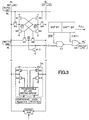
- Fig. 3 is a diagram showing a portion of the logic employed in the invention for word masking and word or array resetting.
- Referring to Fig. 1 the CAM cell array 11 of the present invention is organized in N-bit wide words and M words deep. A typical, but not limiting, example comprises an array of 48 bit words, with 256 such words in the array. Two extra bits (skip bit and empty bit) are attached to each word for word masking and reset purposes. Connected to each bit in the array through lines BL and

Descriptor circuitry 1 exchanges data with a 16bit bus 10. Arow decoder 2 is connected to array 11 through a bus containing a plurality of word lines WL for selecting different words in the array. A bit-line precharge circuit 3 is connected to array 11 through a plurality of bit lines BL and BL, a pair of such bit lines being provided for each column of bits in the array. Communicating with the output of array 11 through match lines ML are a word masking and resetcircuit 4, amatch detector 5 and apriority encoder 6. Acontrol logic network 7 provides inputs tocircuits bus 10.Circuits bus 10, the communication betweenbus 10 andcircuit 4 being bidirectional. The details of these circuits are shown in more detail in Fig. 2. - The most important feature of the overall architecture of the CAM system in accordance with the present invention are shown in Fig. 2. The elements of bit-
line descriptor circuitry 1 from Fig. 1 are shown in the dottedenclosure 1 and include aCAM register 17, a mask register 18, acompound register 19, asense amplifier 14 and a programmable bit line writing circuit included in adescriptor element 36. - The circuit of Fig. 2 also shows an address decoder 30 corresponding in function to row
decoder 2 of Fig. 1 to decode the eight address bits supplied frombus 10 to identify the one of the 256 words in array 11 to be selected. Also shown connected to the output of array 11 and to decoder 30 are askip bit array 22 having askip write circuit 20, and anempty bit array 24 having anempty write circuit 23. Outputs fromelements empty bits element 41. - Also shown in Fig. 2 are a
full detector 31 controlled by afull control element 37 and supplying an output to astatus register 40 and to afull register 32.Status register 40 communicates in a 16 bit manner withbus 10 during a status read operation. - A
match detector 28 controlled by amatch control element 38 supplies a single match signal to amatch register 29. Signals fromfull register 32 and match register 29 are supplied tofull flag element 26 andmatch flag element 27, respectively.Match detector 28 also supplies both the single match signal and a multiple match signal tostatus register 40. - Fig. 2 also shows a
priority multiplexor 25 which multiplexes the information fromelements multiplexor control element 33. Asegment counter 34 is under the control of acounter control element 35 which is connected tobus 10 and to the output ofOP code generator 39.Counter 34 supplies one input to status register 40 and another output to an output field selector and data readelement 42. - The system of the present invention has four modes of operation, which are command write (CW), data write (DW), status read (SR), and data read (DR), as shown by the corresponding blocks on the output of a
mode generator 13 in Fig. 2. In the data write mode, data is written into the comparand register.Mode generator 13 receives a chip enable signal on a pin


Comparand register 19 is the main buffer betweenbus 10 and CAM array 11. After a data write operation is performed, one of the operation (OP) codes is carried out under the control of the command write cycle to move data into CAM array 11 ormask register 17. - Under the command write cycle the command write instruction is encoded on the 16
bit bus 10. Of the 16 bits onbus bus 10 for the address location to indicate to which location in array 11 the data is to be transferred fromcomparand register 19. The OP codes employed in the present invention are listed below.
Op Code 0 Initialization
All Skip-bits are set to LOW (don't skip) and all Empty-bits are set to HIGH (empty). The /MTCH and /FULL outputs are enabled. The mode is set to 48-bit mode. The Mask register and Segment counter are reset to zero. By default, subsequent data writes and reads are to and from the comparand register.
Op Code 1 Output control
Match and full flags are enabled or disabled by this command.
Op Code 2 Mode select
User can use this command to select between 16 or 48 bit mode. In 16-bit mode, the Segment counter is never incremented.
Op Code 3 Move Comparand Register to Mask Register
Contents of the Comparand register data is moved into the Mask register.
Op Code 4 Move Mask Register to Comparand Register
Contents of the Mask register data is moved into the comparand register.
Op Code 5 Enable Output from Skip and Empty Bit Array to I/O port
All subsequent data mode reads result in data flowing from Empty-bits and Skip-bits to the output buffer. Address is specified by the command register address field.
Op Code 6 Move Comparand Register to CAM
Contents of the Comparand register data is moved into the CAM. The Empty-bit and Skip-bit are not changed. The CAM address is specified by the command word address field. The Segment counter is not changed.
Op Code 7 Move CAM to Comparand Register
Contents of the CAM data specified by the command word
address field is moved into the Comparand register. The Segment counter is not changed. The Skip and Empty Bit Array information is not changed.
Op Code 8 Reserved
Op Code 9 Skip-bit control
User can write to Skip-bit array using this command. They can write the whole array in one cycle or any individual bit by providing the desired address location.
Op Code 10 Empty-bit control
User can write to Empty-bit array using this command. They can write the whole array in one cycle or any individual bit by providing the desired address location.
Op Code 11 Enable Output from Comparand Register to I/O Port
All subsequent data reads result in data flowing from the Comparand register segment to the output buffer.
Op Code 12 Enable Output from Mask Register to I/O port
All subsequent data reads result in data flowing from the Mask register segment to the output buffer.
Op Code 13 Enable Output from CAM to I/O port
All subsequent data reads result in data flowing from the CAM segment to the output buffer. CAM address is specified by the command word address field.
Op Code 14 Move Ccmparand Register to CAM (Reset Empty bit and Skip bit both LOW)
Contents of the comparand register data is moved into address specified by the command word address field (CAM address). The corresponding Empty bit and Skip bit are both reset to LOW.
Op Code 15 Load Segment Counter
User can change the segment counter to get to any one of the 3 segments. - These 16 OP-code instructions are encoded by 4 high order bits of a command word on the 16 bit bus. A typical command word looks like:

- A status read is normally an operation following a match operation where the user wants to know the match location, whether it's a multiple or single match, and if the chip is still full. The contents of
status register 40 can be read out ontobus 10. Two bits can be read fromsegment counter 22, eight bits from the address position indication frompriority encoder 21 and three flag bits fromfull detector 31 and from the match andmultiple match detector 28. - The status word employed in the present invention can be described as follows: As shown below, the lower eight bit of the status word are the encoded address to indicate to the user the location.

- The upper three bits identify the status flags, including a multiple match flag, a full flag and a match flag. These internal flags should be like the external ones, but if outputs are not enabled, the flags will be high.
- Data Read is a read operation where the user can obtain information from
CAM register 17, from compareregister 19, from mask register 18 or from the skip and empty bit information frommemory 41. Hence, a Data Read operation will read information from one of the four registers depending on the previous command write cycle. - Two status bits are employed with each word in the present invention; one is a skip bit and the other is termed an empty bit. The skip bit is employed to enable the user to mask out a word and the empty bit is used in connection with empty bit locations in the array.
- The invention employs a
priority encoder 21 to provide an indication of the highest priority address location. For a match operation where a whole array compare is performed, this feature will provide an indication of the match location if there is a match. If there is not a match, thepriority encoder 21 will point to the next empty address available for use. Under the multiple match condition in which there are more than 1 match locations the user can mask out, word by word until he can identify all locations having matched, this being the function of the skip bit represented byskip bit circuitry 20 and theskip bit array 22. Another bit employed herein is the empty bit, represented byempty write circuitry 23 andempty bit array 24. The empty bit has two states, one of which is empty and the other is full. The particular word location is used so that the user can set the empty bit to show that this particular bit location is occupied. Thus, when the user wants to write into the CAM cell he will know that some of the locations therein already have data in them. -
Segment counter 34 keeps track of the internal segments so that the 16bit bus 10 can be used for a 48 bit operation. At the start of a 16 bit mode operation the segment count incounter 34 is always set to the first count. However, there is also a user programmable feature by which the user can advance to the second segment count or the third segment count by using OP codes 15, described above. - There are two external flags, one of which is the "full" flag, represented by
element 26, and the other is the "match" flag, represented byelement 27. If there is a match in the array, as detected bymatch detector 28 and communicated throughmatch register 29 toflag 27, the match flag will go low. Similarly, if all the locations in array 11 are full, as detected byfull detector 31 and communicated throughfull register 32, toflag 26, the full flag will go low. When thefull flag 26 is high, this means there are still empty locations in array 11 for the user, and when thematch flag 27 remains high, this means there is no match. - Signals from both the match line and the full line go into the
priority encoder 21 through priority multiplexer 25 (Fig. 1). If there is no match, the empty location will be decoded as well. Both the empty information and the match information are supplied topriority encoder 21.Full detector 31 will detect whether the array is full or empty. -
Match detector 28 detects a match or no match condition, whereaspriority encoder 21 provides the address location of the match word.Priority encoder multiplexer 25 will multiplex the empty and the match location information, so that one of the two will be coming intoencoder 21. - Referring to Fig. 3, a nine transistor cell is shown of which transistors M1, M2, M5, M6 are the basic storage elements, the cross coupled pairs. Nodes ST and


- When all N bits in the same word have matching data on their respective bit line pairs, a match condition occurs. Since all the cell match nodes are at logic low, none of the pull down transistors M13 on the match line can be turned on. Therefore, the match line will remain at a logic high. In contrast, any nonmatch condition will result in the match line being pulled low.
- When both Bl and


register 19 can appear on the bit line pair. - Word masking can be accomplished by setting either the skip or/and the empty bit high. In either case, the final match line output (ML') will be forced low through the NAND gate (47) and NOR gate (48) indicating a nonmatch condition even if there is a match.
- When all empty bits are set high, all M words are set empty and are available for new data.
Claims (13)
- A content addressable memory system comprising:a plurality of memory cells arranged in rows and columns in an array (11) of N bit words by M word cells;a plurality of word lines (WL) extending through said array for addressing different words in said memory cells each of said words comprising a plurality of adjacent ones of said cells extending in a first direction in said array;a plurality of match lines (ML) extending through said array in parallel with said word lines in said first direction;a plurality of bit lines (BL,BL) extending through said array in a second direction perpendicular to said first direction, each of said bit lines communicating with said cells in one column of said cells extending through said array in said second direction;said bit lines being configured in pairs, with a pair of said bit lines (BL,BL) communicating with each of said cells in each of said columns;means for storing bits in selected ones of said memory cells in said array;an input/output (I/O) bus (10);means for supplying on said I/O bus a match word to be compared with said M words in said array;comparing means (1) for simultaneously comparing the bits of said match word with the bits of said M words in said array;match detecting means (28) for detecting a match condition between said bits in said match word and said bits in said M words in said array;means for masking selectable ones of said match conditions to produce unmasked match word conditions;full detecting means (31) for detecting whether or not the array is full;priority encoder means (21) responsive to said match detection means (28) and said full detecting means (31) characterised in that the priority encoder means is adapted for providing an indication of the match location(s) for said unmasked match word condition(s) in said array and for providing an indication of the next empty address in said array when there is no match condition.
- A memory system as claimed in claim 1, including:a priority multiplexer (25) having an input and an output;means for supplying the outputs of said match detecting means (28) and said full detecting means (31) to said input of said priority multiplexer (25);means for multiplexing said inputs to said priority multiplexer; andmeans for supplying said multiplexed inputs at said output of said priority multiplexer to said priority encoder means (21).
- A memory system as claimed in claim 2, including priority multiplexer control means (33) for controlling said priority multiplexer (25).
- A memory system as claimed in claim 2, including:a status register (40) connected to said I/O bus (10); anda segment counter (34) connected to said status register (40) for controlling the supplying of said match words to said I/O bus.
- A memory system as claimed in claim 1, in which said I/O bus has a bit capacity less than N.
- A memory system as claimed in claim 5, in which said bit capacity of said I/O bus is a submultiple of N.
- A memory system as claimed in claim 1, in which the comparing means includes:bit line descriptor circuitry (1) associated with each of said pairs of bit lines;said bit line descriptor circuitry including:a comparand register (19),a mask register (18),a sense amplifier (14),a programmable bit line writing circuit (36);means (I/O CTRL) for supplying data to be written into said cells from said data bus (10) to said comparand register (19);means for supplying said data to be written from said comparand register (19) to said programmable bit line writing circuit (36); andmeans for supplying said data to be written from said programmable bit line writing circuit (36) to all of said pairs of said bit lines (BL,

- A memory system as claimed in claim 7, including:
means for connecting said sense amplifier (14) to said pair of bit lines (BL,
- A memory system as claimed in claim 7, including:means for performing a masking operation on data to be stored in said cells, said mask performing means including, means for supplying to said mask register (18) selected signal bits corresponding to data bits to be masked in said cells;means for supplying data bits to be stored in said cells;means for comparing said supplied data bits with the contents of said mask register (18) to eliminate from said supplied data bits those bits which correspond to said selected signal bits corresponding to said data bits to be masked; andmeans for communicating said supplied bits remaining after said comparing to said cells.
- A memory system as claimed in claim 9, in which said supplied bits to be stored are transmitted from an I/O bus (10) to said comparand register (19).
- A memory system as claimed in claim 10, in which said selected signal bits corresponding to data to be masked in said cells are transmitted from said comparand register to said mask register (18).
- A system in accordance with claim 11 in which said selected signal bits corresponding to data to be masked in said cells is first transmitted from said I/O bus to said comparand register (19) and then to said mask register (18), and said supplied bits to be stored are transmitted from said I/O bus to said comparand register.
- A systemas claimed in claim 9, in which said comparand register and said mask register (18) have a bit capacity which is a multiple of the bit capacity of said I/O bus.
Applications Claiming Priority (2)
| Application Number | Priority Date | Filing Date | Title |
|---|---|---|---|
| US193315 | 1988-05-11 | ||
| US07/193,315 US4928260A (en) | 1988-05-11 | 1988-05-11 | Content addressable memory array with priority encoder |
Publications (3)
| Publication Number | Publication Date |
|---|---|
| EP0341897A2 EP0341897A2 (en) | 1989-11-15 |
| EP0341897A3 EP0341897A3 (en) | 1992-10-28 |
| EP0341897B1 true EP0341897B1 (en) | 1997-07-30 |
Family
ID=22713125
Family Applications (1)
| Application Number | Title | Priority Date | Filing Date |
|---|---|---|---|
| EP89304467A Expired - Lifetime EP0341897B1 (en) | 1988-05-11 | 1989-05-04 | Content addressable memory array architecture |
Country Status (5)
| Country | Link |
|---|---|
| US (1) | US4928260A (en) |
| EP (1) | EP0341897B1 (en) |
| JP (1) | JP3006715B2 (en) |
| AT (1) | ATE156281T1 (en) |
| DE (1) | DE68928213T2 (en) |
Families Citing this family (82)
| Publication number | Priority date | Publication date | Assignee | Title |
|---|---|---|---|---|
| US5072422A (en) * | 1989-05-15 | 1991-12-10 | E-Systems, Inc. | Content-addressed memory system with word cells having select and match bits |
| JPH03219326A (en) * | 1990-01-24 | 1991-09-26 | Mitsubishi Electric Corp | data comparison circuit |
| DE69132367T2 (en) * | 1990-05-31 | 2001-02-22 | Stmicroelectronics, Inc. | Content addressable memory |
| US5123105A (en) * | 1990-06-25 | 1992-06-16 | Advanced Micro Devices, Inc. | Priority encoder for a content addressable memory |
| US5491806A (en) * | 1990-06-26 | 1996-02-13 | Lsi Logic Corporation | Optimized translation lookaside buffer slice having stored mask bits |
| SE9002558D0 (en) * | 1990-08-02 | 1990-08-02 | Carlstedt Elektronik Ab | PROCESSOR |
| US5319763A (en) * | 1991-04-02 | 1994-06-07 | Motorola, Inc. | Data processor with concurrent static and dynamic masking of operand information and method therefor |
| JP3015493B2 (en) * | 1991-04-26 | 2000-03-06 | 株式会社東芝 | Semiconductor associative memory |
| US5249152A (en) * | 1991-06-20 | 1993-09-28 | Unisys Corporation | Bookkeeping memory |
| JP2728819B2 (en) * | 1991-12-18 | 1998-03-18 | 川崎製鉄株式会社 | Semiconductor integrated circuit |
| US5999434A (en) | 1992-01-10 | 1999-12-07 | Kawasaki Steel Corporation | Hierarchical encoder including timing and data detection devices for a content addressable memory |
| US5619446A (en) * | 1992-01-10 | 1997-04-08 | Kawasaki Steel Corporation | Hierarchical encoder including timing and data detection devices for a content addressable memory |
| FR2687004B1 (en) * | 1992-01-31 | 1994-03-18 | France Telecom | ASSOCIATIVE MEMORY ARCHITECTURE. |
| US5257220A (en) * | 1992-03-13 | 1993-10-26 | Research Foundation Of The State Univ. Of N.Y. | Digital data memory unit and memory unit array |
| US5351208A (en) * | 1992-04-27 | 1994-09-27 | Integrated Information Technology, Inc. | Content addressable memory |
| US5383146A (en) * | 1992-06-08 | 1995-01-17 | Music Semiconductors, Inc. | Memory with CAM and RAM partitions |
| US5454094A (en) * | 1993-06-24 | 1995-09-26 | Hal Computer Systems, Inc. | Method and apparatus for detecting multiple matches in a content addressable memory |
| SG44604A1 (en) * | 1993-09-20 | 1997-12-19 | Codex Corp | Circuit and method of interconnecting content addressable memory |
| US5586288A (en) * | 1993-09-22 | 1996-12-17 | Hilevel Technology, Inc. | Memory interface chip with rapid search capability |
| FR2713797B1 (en) * | 1993-12-13 | 1996-02-09 | Matra Mhs | Access protocol controller by a central unit to peripheral units. |
| US5491757A (en) * | 1993-12-22 | 1996-02-13 | Humphrey Instruments, Inc. | Field tester gaze tracking using content addressable memories to improve image data analysis speed |
| US6122706A (en) * | 1993-12-22 | 2000-09-19 | Cypress Semiconductor Corporation | Dual-port content addressable memory |
| US5649149A (en) * | 1994-08-01 | 1997-07-15 | Cypress Semiconductor Corporation | Integrated content addressable memory array with processing logical and a host computer interface |
| US5860085A (en) * | 1994-08-01 | 1999-01-12 | Cypress Semiconductor Corporation | Instruction set for a content addressable memory array with read/write circuits and an interface register logic block |
| US5646878A (en) * | 1995-06-02 | 1997-07-08 | Motorola, Inc. | Content addressable memory system |
| US5964857A (en) * | 1997-05-30 | 1999-10-12 | Quality Semiconductor, Inc. | Priority encoder for a content addressable memory system |
| US6148364A (en) * | 1997-12-30 | 2000-11-14 | Netlogic Microsystems, Inc. | Method and apparatus for cascading content addressable memory devices |
| US6199140B1 (en) * | 1997-10-30 | 2001-03-06 | Netlogic Microsystems, Inc. | Multiport content addressable memory device and timing signals |
| EP0936625A3 (en) | 1998-02-17 | 2003-09-03 | Texas Instruments Incorporated | Content addressable memory (CAM) |
| US6240485B1 (en) | 1998-05-11 | 2001-05-29 | Netlogic Microsystems, Inc. | Method and apparatus for implementing a learn instruction in a depth cascaded content addressable memory system |
| US6219748B1 (en) | 1998-05-11 | 2001-04-17 | Netlogic Microsystems, Inc. | Method and apparatus for implementing a learn instruction in a content addressable memory device |
| US6381673B1 (en) * | 1998-07-06 | 2002-04-30 | Netlogic Microsystems, Inc. | Method and apparatus for performing a read next highest priority match instruction in a content addressable memory device |
| US6266262B1 (en) | 1998-11-05 | 2001-07-24 | Lara Technology, Inc. | Enhanced binary content addressable memory for longest prefix address matching |
| US6081440A (en) * | 1998-11-05 | 2000-06-27 | Lara Technology, Inc. | Ternary content addressable memory (CAM) having fast insertion and deletion of data values |
| US6237061B1 (en) | 1999-01-05 | 2001-05-22 | Netlogic Microsystems, Inc. | Method for longest prefix matching in a content addressable memory |
| US6574702B2 (en) | 1999-02-23 | 2003-06-03 | Netlogic Microsystems, Inc. | Method and apparatus for determining an exact match in a content addressable memory device |
| US6460112B1 (en) | 1999-02-23 | 2002-10-01 | Netlogic Microsystems, Llc | Method and apparatus for determining a longest prefix match in a content addressable memory device |
| US6539455B1 (en) | 1999-02-23 | 2003-03-25 | Netlogic Microsystems, Inc. | Method and apparatus for determining an exact match in a ternary content addressable memory device |
| US6499081B1 (en) | 1999-02-23 | 2002-12-24 | Netlogic Microsystems, Inc. | Method and apparatus for determining a longest prefix match in a segmented content addressable memory device |
| US6892272B1 (en) | 1999-02-23 | 2005-05-10 | Netlogic Microsystems, Inc. | Method and apparatus for determining a longest prefix match in a content addressable memory device |
| US6420990B1 (en) | 1999-03-19 | 2002-07-16 | Lara Technology, Inc. | Priority selection circuit |
| US6137707A (en) * | 1999-03-26 | 2000-10-24 | Netlogic Microsystems | Method and apparatus for simultaneously performing a plurality of compare operations in content addressable memory device |
| US6317349B1 (en) | 1999-04-16 | 2001-11-13 | Sandisk Corporation | Non-volatile content addressable memory |
| US6157558A (en) * | 1999-05-21 | 2000-12-05 | Sandisk Corporation | Content addressable memory cell and array architectures having low transistor counts |
| US6166938A (en) * | 1999-05-21 | 2000-12-26 | Sandisk Corporation | Data encoding for content addressable memories |
| US6505270B1 (en) | 1999-07-02 | 2003-01-07 | Lara Technology, Inc. | Content addressable memory having longest prefix matching function |
| US6944709B2 (en) * | 1999-09-23 | 2005-09-13 | Netlogic Microsystems, Inc. | Content addressable memory with block-programmable mask write mode, word width and priority |
| US7487200B1 (en) | 1999-09-23 | 2009-02-03 | Netlogic Microsystems, Inc. | Method and apparatus for performing priority encoding in a segmented classification system |
| US7272027B2 (en) * | 1999-09-23 | 2007-09-18 | Netlogic Microsystems, Inc. | Priority circuit for content addressable memory |
| US6934795B2 (en) * | 1999-09-23 | 2005-08-23 | Netlogic Microsystems, Inc. | Content addressable memory with programmable word width and programmable priority |
| US7143231B1 (en) | 1999-09-23 | 2006-11-28 | Netlogic Microsystems, Inc. | Method and apparatus for performing packet classification for policy-based packet routing |
| US6542391B2 (en) * | 2000-06-08 | 2003-04-01 | Netlogic Microsystems, Inc. | Content addressable memory with configurable class-based storage partition |
| US7110407B1 (en) | 1999-09-23 | 2006-09-19 | Netlogic Microsystems, Inc. | Method and apparatus for performing priority encoding in a segmented classification system using enable signals |
| US6795892B1 (en) | 2000-06-14 | 2004-09-21 | Netlogic Microsystems, Inc. | Method and apparatus for determining a match address in an intra-row configurable cam device |
| US6567340B1 (en) | 1999-09-23 | 2003-05-20 | Netlogic Microsystems, Inc. | Memory storage cell based array of counters |
| US6751701B1 (en) | 2000-06-14 | 2004-06-15 | Netlogic Microsystems, Inc. | Method and apparatus for detecting a multiple match in an intra-row configurable CAM system |
| US6757779B1 (en) | 1999-09-23 | 2004-06-29 | Netlogic Microsystems, Inc. | Content addressable memory with selectable mask write mode |
| US6799243B1 (en) | 2000-06-14 | 2004-09-28 | Netlogic Microsystems, Inc. | Method and apparatus for detecting a match in an intra-row configurable cam system |
| US6647457B1 (en) | 1999-11-16 | 2003-11-11 | Cypress Semiconductor Corporation | Content addressable memory having prioritization of unoccupied entries |
| US6591331B1 (en) * | 1999-12-06 | 2003-07-08 | Netlogic Microsystems, Inc. | Method and apparatus for determining the address of the highest priority matching entry in a segmented content addressable memory device |
| US6839795B1 (en) * | 2000-05-31 | 2005-01-04 | Silicon Labs Cp, Inc. | Priority cross-bar decoder |
| US7171542B1 (en) * | 2000-06-19 | 2007-01-30 | Silicon Labs Cp, Inc. | Reconfigurable interface for coupling functional input/output blocks to limited number of i/o pins |
| DE60211761T2 (en) * | 2001-01-19 | 2007-05-24 | President Of Hiroshima University, Higashihiroshima | Content-Addressable Semiconductor Memory |
| US6910097B1 (en) | 2001-04-09 | 2005-06-21 | Netlogic Microsystems, Inc. | Classless interdomain routing using binary content addressable memory |
| JP3881869B2 (en) * | 2001-11-05 | 2007-02-14 | 株式会社ルネサステクノロジ | Semiconductor memory device |
| AU2002214240A1 (en) * | 2001-11-05 | 2003-06-10 | Hywire Ltd. | Ram-based range content addressable memory |
| US6671218B2 (en) * | 2001-12-11 | 2003-12-30 | International Business Machines Corporation | System and method for hiding refresh cycles in a dynamic type content addressable memory |
| US7301961B1 (en) | 2001-12-27 | 2007-11-27 | Cypress Semiconductor Corportion | Method and apparatus for configuring signal lines according to idle codes |
| US7171595B1 (en) * | 2002-05-28 | 2007-01-30 | Netlogic Microsystems, Inc. | Content addressable memory match line detection |
| US7401181B1 (en) | 2002-05-29 | 2008-07-15 | Core Networks Llc | System and method for comparand reuse |
| US7272684B1 (en) | 2002-06-26 | 2007-09-18 | Netlogic Microsystems, Inc. | Range compare circuit for search engine |
| US7206212B1 (en) | 2002-08-13 | 2007-04-17 | Netlogic Microsystems, Inc. | Content addressable memory (CAM) device with entries having ternary match and range compare functions |
| US6577520B1 (en) | 2002-10-21 | 2003-06-10 | Integrated Device Technology, Inc. | Content addressable memory with programmable priority weighting and low cost match detection |
| US6804132B2 (en) * | 2002-11-25 | 2004-10-12 | International Business Machines Corporation | Circuit for multiple match hit CAM readout |
| US6864810B2 (en) * | 2003-07-24 | 2005-03-08 | Micron Technology, Inc. | Converting digital signals |
| US6831587B1 (en) | 2003-07-31 | 2004-12-14 | Micron Technology, Inc. | Priority encoding |
| US7152141B2 (en) * | 2003-07-31 | 2006-12-19 | Micron Technology, Inc. | Obtaining search results for content addressable memory |
| US7436688B1 (en) | 2005-05-06 | 2008-10-14 | Netlogic Microsystems, Inc. | Priority encoder circuit and method |
| US7570503B1 (en) | 2005-05-20 | 2009-08-04 | Netlogic Microsystems, Inc. | Ternary content addressable memory (TCAM) cells with low signal line numbers |
| US8717793B2 (en) | 2009-05-26 | 2014-05-06 | Arizona Board Of Regents, For And On Behalf Of Arizona State University | Longest prefix match internet protocol content addressable memories and related methods |
| US8438330B2 (en) | 2010-05-17 | 2013-05-07 | Netlogic Microsystems, Inc. | Updating cam arrays using prefix length distribution prediction |
| US20230100785A1 (en) * | 2021-09-28 | 2023-03-30 | Nvidia Corporation | Priority encoder-based techniques for computing the minimum or the maximum of multiple values |
Family Cites Families (9)
| Publication number | Priority date | Publication date | Assignee | Title |
|---|---|---|---|---|
| US3195109A (en) * | 1962-04-02 | 1965-07-13 | Ibm | Associative memory match indicator control |
| US3633182A (en) * | 1969-08-26 | 1972-01-04 | Bell Telephone Labor Inc | Content addressable memory cell |
| US4065756A (en) * | 1976-03-15 | 1977-12-27 | Burroughs Corporation | Associative memory with neighboring recirculated paths offset by one bit |
| DE2712575C2 (en) * | 1977-03-22 | 1985-12-19 | Walter Dipl.-Ing. 8011 Putzbrunn Motsch | Associative storage system in highly integrated semiconductor technology |
| US4296475A (en) * | 1978-12-19 | 1981-10-20 | U.S. Philips Corporation | Word-organized, content-addressable memory |
| US4404653A (en) * | 1981-10-01 | 1983-09-13 | Yeda Research & Development Co. Ltd. | Associative memory cell and memory unit including same |
| US4670858A (en) * | 1983-06-07 | 1987-06-02 | Tektronix, Inc. | High storage capacity associative memory |
| US4794559A (en) * | 1984-07-05 | 1988-12-27 | American Telephone And Telegraph Company, At&T Bell Laboratories | Content addressable semiconductor memory arrays |
| US4723224A (en) * | 1986-01-02 | 1988-02-02 | Motorola, Inc. | Content addressable memory having field masking |
-
1988
- 1988-05-11 US US07/193,315 patent/US4928260A/en not_active Expired - Lifetime
-
1989
- 1989-05-04 DE DE68928213T patent/DE68928213T2/en not_active Expired - Fee Related
- 1989-05-04 AT AT89304467T patent/ATE156281T1/en active
- 1989-05-04 EP EP89304467A patent/EP0341897B1/en not_active Expired - Lifetime
- 1989-05-10 JP JP1117162A patent/JP3006715B2/en not_active Expired - Fee Related
Also Published As
| Publication number | Publication date |
|---|---|
| ATE156281T1 (en) | 1997-08-15 |
| EP0341897A3 (en) | 1992-10-28 |
| DE68928213D1 (en) | 1997-09-04 |
| EP0341897A2 (en) | 1989-11-15 |
| DE68928213T2 (en) | 1998-02-26 |
| US4928260A (en) | 1990-05-22 |
| JP3006715B2 (en) | 2000-02-07 |
| JPH0271497A (en) | 1990-03-12 |
Similar Documents
| Publication | Publication Date | Title |
|---|---|---|
| EP0341897B1 (en) | Content addressable memory array architecture | |
| US4890260A (en) | Content addressable memory array with maskable and resettable bits | |
| EP0341896B1 (en) | Content addressable memory array | |
| US4975873A (en) | Content addressable memory with flag storage to indicate memory state | |
| US5752260A (en) | High-speed, multiple-port, interleaved cache with arbitration of multiple access addresses | |
| US5319763A (en) | Data processor with concurrent static and dynamic masking of operand information and method therefor | |
| US5890201A (en) | Content addressable memory having memory cells storing don't care states for address translation | |
| US4654781A (en) | Byte addressable memory for variable length instructions and data | |
| US6137707A (en) | Method and apparatus for simultaneously performing a plurality of compare operations in content addressable memory device | |
| US7404066B2 (en) | Active memory command engine and method | |
| US5341500A (en) | Data processor with combined static and dynamic masking of operand for breakpoint operation | |
| US8341328B2 (en) | Method and system for local memory addressing in single instruction, multiple data computer system | |
| US4685080A (en) | Microword generation mechanism utilizing separate programmable logic arrays for first and second microwords | |
| US5220526A (en) | Method and apparatus for indicating a duplication of entries in a content addressable storage device | |
| US5390139A (en) | Devices, systems and methods for implementing a Kanerva memory | |
| GB2244157A (en) | Apparatus for row caching in random access memory | |
| WO1991007754A1 (en) | Read-while-write-memory | |
| GB2108737A (en) | Byte addressable memory for variable length instructions and data | |
| US4982379A (en) | Semiconductor memory device having associative function | |
| US4931989A (en) | Microword generation mechanism utilizing a separate programmable logic array for first microwords | |
| US4404629A (en) | Data processing system with latch for sharing instruction fields | |
| JP2564942B2 (en) | Selective associative memory device and control method thereof | |
| US5485588A (en) | Memory array based data reorganizer | |
| JPH01290194A (en) | Selective associative storage and control system | |
| HK1003851A1 (en) | A memory apparatus and method for use in a data processing system |
Legal Events
| Date | Code | Title | Description |
|---|---|---|---|
| PUAI | Public reference made under article 153(3) epc to a published international application that has entered the european phase |
Free format text: ORIGINAL CODE: 0009012 |
|
| AK | Designated contracting states |
Kind code of ref document: A2 Designated state(s): AT BE CH DE ES FR GB GR IT LI LU NL SE |
|
| PUAL | Search report despatched |
Free format text: ORIGINAL CODE: 0009013 |
|
| AK | Designated contracting states |
Kind code of ref document: A3 Designated state(s): AT BE CH DE ES FR GB GR IT LI LU NL SE |
|
| 17P | Request for examination filed |
Effective date: 19930201 |
|
| 17Q | First examination report despatched |
Effective date: 19941025 |
|
| GRAG | Despatch of communication of intention to grant |
Free format text: ORIGINAL CODE: EPIDOS AGRA |
|
| GRAH | Despatch of communication of intention to grant a patent |
Free format text: ORIGINAL CODE: EPIDOS IGRA |
|
| GRAH | Despatch of communication of intention to grant a patent |
Free format text: ORIGINAL CODE: EPIDOS IGRA |
|
| GRAA | (expected) grant |
Free format text: ORIGINAL CODE: 0009210 |
|
| AK | Designated contracting states |
Kind code of ref document: B1 Designated state(s): AT BE CH DE ES FR GB GR IT LI LU NL SE |
|
| PG25 | Lapsed in a contracting state [announced via postgrant information from national office to epo] |
Ref country code: IT Free format text: LAPSE BECAUSE OF FAILURE TO SUBMIT A TRANSLATION OF THE DESCRIPTION OR TO PAY THE FEE WITHIN THE PRE;WARNING: LAPSES OF ITALIAN PATENTS WITH EFFECTIVE DATE BEFORE 2007 MAY HAVE OCCURRED AT ANY TIME BEFORE 2007. THE CORRECT EFFECTIVE DATE MAY BE DIFFERENT FROM THE ONE RECORDED.SCRIBED TIME-LIMIT Effective date: 19970730 Ref country code: LI Free format text: LAPSE BECAUSE OF FAILURE TO SUBMIT A TRANSLATION OF THE DESCRIPTION OR TO PAY THE FEE WITHIN THE PRESCRIBED TIME-LIMIT Effective date: 19970730 Ref country code: GR Free format text: LAPSE BECAUSE OF FAILURE TO SUBMIT A TRANSLATION OF THE DESCRIPTION OR TO PAY THE FEE WITHIN THE PRESCRIBED TIME-LIMIT Effective date: 19970730 Ref country code: BE Effective date: 19970730 Ref country code: AT Effective date: 19970730 Ref country code: CH Free format text: LAPSE BECAUSE OF FAILURE TO SUBMIT A TRANSLATION OF THE DESCRIPTION OR TO PAY THE FEE WITHIN THE PRESCRIBED TIME-LIMIT Effective date: 19970730 Ref country code: ES Free format text: THE PATENT HAS BEEN ANNULLED BY A DECISION OF A NATIONAL AUTHORITY Effective date: 19970730 |
|
| REF | Corresponds to: |
Ref document number: 156281 Country of ref document: AT Date of ref document: 19970815 Kind code of ref document: T |
|
| REG | Reference to a national code |
Ref country code: CH Ref legal event code: EP |
|
| REF | Corresponds to: |
Ref document number: 68928213 Country of ref document: DE Date of ref document: 19970904 |
|
| PG25 | Lapsed in a contracting state [announced via postgrant information from national office to epo] |
Ref country code: SE Effective date: 19971030 |
|
| ET | Fr: translation filed | ||
| REG | Reference to a national code |
Ref country code: CH Ref legal event code: PL |
|
| PG25 | Lapsed in a contracting state [announced via postgrant information from national office to epo] |
Ref country code: LU Free format text: LAPSE BECAUSE OF NON-PAYMENT OF DUE FEES Effective date: 19980504 |
|
| PLBE | No opposition filed within time limit |
Free format text: ORIGINAL CODE: 0009261 |
|
| STAA | Information on the status of an ep patent application or granted ep patent |
Free format text: STATUS: NO OPPOSITION FILED WITHIN TIME LIMIT |
|
| 26N | No opposition filed | ||
| REG | Reference to a national code |
Ref country code: GB Ref legal event code: IF02 |
|
| PGFP | Annual fee paid to national office [announced via postgrant information from national office to epo] |
Ref country code: NL Payment date: 20020325 Year of fee payment: 14 |
|
| PGFP | Annual fee paid to national office [announced via postgrant information from national office to epo] |
Ref country code: GB Payment date: 20020404 Year of fee payment: 14 |
|
| PGFP | Annual fee paid to national office [announced via postgrant information from national office to epo] |
Ref country code: FR Payment date: 20020503 Year of fee payment: 14 |
|
| PGFP | Annual fee paid to national office [announced via postgrant information from national office to epo] |
Ref country code: DE Payment date: 20020531 Year of fee payment: 14 |
|
| PG25 | Lapsed in a contracting state [announced via postgrant information from national office to epo] |
Ref country code: GB Free format text: LAPSE BECAUSE OF NON-PAYMENT OF DUE FEES Effective date: 20030504 |
|
| PG25 | Lapsed in a contracting state [announced via postgrant information from national office to epo] |
Ref country code: NL Free format text: LAPSE BECAUSE OF NON-PAYMENT OF DUE FEES Effective date: 20031201 |
|
| PG25 | Lapsed in a contracting state [announced via postgrant information from national office to epo] |
Ref country code: DE Free format text: LAPSE BECAUSE OF NON-PAYMENT OF DUE FEES Effective date: 20031202 |
|
| GBPC | Gb: european patent ceased through non-payment of renewal fee |
Effective date: 20030504 |
|
| PG25 | Lapsed in a contracting state [announced via postgrant information from national office to epo] |
Ref country code: FR Free format text: LAPSE BECAUSE OF NON-PAYMENT OF DUE FEES Effective date: 20040130 |
|
| NLV4 | Nl: lapsed or anulled due to non-payment of the annual fee |
Effective date: 20031201 |
|
| REG | Reference to a national code |
Ref country code: FR Ref legal event code: ST |