EP0336679A2 - BIC-Speicherzellenstruktur und Herstellungsverfahren dafür - Google Patents
BIC-Speicherzellenstruktur und Herstellungsverfahren dafür Download PDFInfo
- Publication number
- EP0336679A2 EP0336679A2 EP89303271A EP89303271A EP0336679A2 EP 0336679 A2 EP0336679 A2 EP 0336679A2 EP 89303271 A EP89303271 A EP 89303271A EP 89303271 A EP89303271 A EP 89303271A EP 0336679 A2 EP0336679 A2 EP 0336679A2
- Authority
- EP
- European Patent Office
- Prior art keywords
- insulating layer
- opening
- wiring electrode
- doped region
- substrate
- Prior art date
- Legal status (The legal status is an assumption and is not a legal conclusion. Google has not performed a legal analysis and makes no representation as to the accuracy of the status listed.)
- Granted
Links
Images


Classifications
-
- H—ELECTRICITY
- H10—SEMICONDUCTOR DEVICES; ELECTRIC SOLID-STATE DEVICES NOT OTHERWISE PROVIDED FOR
- H10B—ELECTRONIC MEMORY DEVICES
- H10B69/00—Erasable-and-programmable ROM [EPROM] devices not provided for in groups H10B41/00 - H10B63/00, e.g. ultraviolet erasable-and-programmable ROM [UVEPROM] devices
-
- G—PHYSICS
- G11—INFORMATION STORAGE
- G11C—STATIC STORES
- G11C17/00—Read-only memories programmable only once; Semi-permanent stores, e.g. manually-replaceable information cards
-
- H10W20/0698—
Definitions
- the present invention generally relates to programmable memory cell devices and more particularly to a so-called BIC memory cell device and a manufacturing method thereof.
- a BIC (Breakdown-of-Insulator-for-Conduction) memory cell device is a programmable memory cell device comprising a MOS transistor having a drain region connected to a bit line via a thin insulator film and a source region connected to the ground (see for example, Sato N. et al. A New Programmable Cell Utilizing Insulator Breakdown. IEDM 85, pp.639 - 642, IEEE (1985).
- the gate of the MOS transistor is connected to a word line and the writing of a data is made by causing a breakdown in the thin insulator film by applying a high voltage to a selected bit line while at the same time applying a predetermined voltage to a selected word line.
- This high voltage is chosen such that the thin insulator film is destroyed with reliability at this voltage.
- the drain of the MOS transistor is connected directly to the bit line.
- another bit line voltage substantially lower than the first bit line voltage is applied to a selected bit line while applying the predetermined word line voltage to a selected word line.
- This second bit line voltage is chosen such that the breakdown of the thin insulator film does not occur even when such a voltage is applied to the bit line.
- Such a device has a simple structure and easily manufactured in a form of integrated circuit. Further, it can be manufactured by a step which is almost the same as the manufacturing step of a dynamic random access memory and thus the manufacturing cost can be reduced. Further, such a memory device is more reliable as compared to conventional programmable read only memories using fuse as the means for writing the data. Furthermore, the BIC memory cell device has a writing speed of less than 1 ⁇ sec which is faster than any other programmable read only memories available at the present time.
- the conventional BIC memory cell device uses holes having the blunted cross section as already described.
- holes for the source region and for the drain region are usually formed at the same time by etching.
- the sharp edge of the holes thus formed are then blunted by annealing.
- the blunted cross section is not necessary for the hole for the source region which is connected directly to the ground, and as such a blunted cross section occupies a substantial area in the substrate, there is a problem in the conventional BIC memory device that the memory cell device manufactured by such a process has an unnecessarily large size and is therefore disadvantageous for increasing an integration density when a memory cell array is constructed by assembling numerous BIC memory cell devices in a form of integrated circuit.
- Another and more specific object of the present invention is to provide a BIC memory cell device and a manufacturing method thereof wherein the size of the BIC memory cell device can be substantially reduced.
- Another object of the present invention is to provide a manufacturing method of a BIC memory cell device having a substantially reduced size wherein the number of steps needed for producing the device is reduced.
- Another object of the present invention is to provide a BIC memory cell device and a manufacturing method thereof in which a MOS transistor having a drain region connected to a bit line via a thin insulator film and a source region connected to the ground is formed on a substrate, and an edge of a first penetrating hole, provided in an insulator layer on the substrate in correspondence to the drain region for allowing the connection of the bit line to the drain region via the thin insulator film, is blunted while a second penetrating hole, provided in the insulator layer in correspondence to the source region for allowing the connection of the source region to the ground, is made to have a sharp edge.
- the premature breakdown of the thin insulator film at the time of reading out the data and the like is eliminated as a result of the use of the blunted edge for the first hole.
- the size of the BIC memory cell can be reduced as a result of the use of the second hole having a sharp edge.
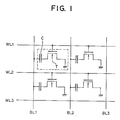
- FIG.1 shows a general structure of a BIC memory cell device.
- a BIC memory cell device is essentially a MOS transistor T having a source connected to the ground, a drain connected to a bit line such as BL1 via an insulator film C , and a gate connected to a word line such as WL1.
- a predetermined word line voltage is applied to a selected word line such as WL1 and at the same time a high first bit line voltage is applied to a selected bit line such as BL1.
- the drain of the MOS transistor T is connected to the ground.
- a high bit line voltage is applied directly across the insulator film C and a breakdown is caused in the insulator film C . Responsive to the breakdown of the insulator film C , the data "1" is written into the BIC memory cell device.
- a second bit line voltage which is substantially lower than the first bit line voltage is applied to the selected bit line together with simultaneous application of the predetermined word line voltage to the selected word line.
- the addressed memory cell is the one already written with the data "1”
- the bit line is connected to the ground through the MOS transistor T and the bit line voltage assumes a low level state.
- the addressed memory cell is the one not written with the data "1" which means that the data stored in the memory cell device is "0"
- the bit line voltage assumes a high level state indicating that the addressed data is zero.
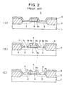
- a MOS structure T comprising a source region 2, a drain region 3 and a gate electrode 4 is formed on a silicon substrate 1.
- the MOS structure may be the structure of a p-channel MOS transistor or an n-channel MOS transistor.
- the substrate 1 is doped to the n-type and the source region 2 and the drain region 3 are doped to the p+-type.
- the substrate 1 is doped to the p-type and the source region 2 and the drain region 3 are doped to the n+-type.
- the MOS transistor T is separated from adjacent MOS transistors (not shown) by a field isolating structure 5 which may be a silicon oxide layer formed on the substrate 1 by oxidization of the substrate 1.
- the gate electrode 4 is separated from the substrate 1 by a gate oxide layer 4a and the entire structure including the source region 2, the drain region 3, the gate electrode 4 and the isolating silicon oxide layer 5 are covered by a protective glass layer 6 which may be a phospho-silicate glass (PSG).
- PSG phospho-silicate glass
- the layer 6 is made of the phospho-silicate glass and will be referred to as PSG layer 6. It should be noted, however, that the material for the layer 6 is not limited to PSG but other materials such as silica may be used as well.
- penetrating holes 7, 8 and 9 are formed through the PSG layer 6 in correspondence to the source region 2, the drain region 3 and the gate electrode 4.
- These holes may be formed by anisotropic etching such as reactive ion etching and is defined by walls 7a, 8a and 9a which extend perpendicularly to the substrate 1. It should be noted that these holes 7, 8 and 9 have sharply defined edges 7b, 8b and 9b at a rim of the respective holes.
- the structure thus formed is subjected to heat treatment in a step of FIG.2(C) and the sharp edges 7b, 8b and 9b at the rim of the holes 7, 8 and 9 are blunted as shown in by inclined walls 7c, 8c and 9c in FIG.2(C).
- an insulator film 10 such as silicon nitride Si3N4 is deposited on the entire structure uniformly as shown in FIG.2(D). Further, the insulator film 10 is removed except for the drain region 3 by etching as shown in FIG.2(E).
- a wiring conductor layer 11 is deposited over the entire structure in a step of FIG.2(F). Finally, the wiring conductor layer 11 is patterned in a step of FIG.2(G) and a wiring electrode 12 for the source region 2, a wiring electrode 13 for the gate electrode 4 and a wiring electrode 14 for the drain region 3 are formed.
- the premature breakdown of the insulator film 10 is prevented by depositing the film 10 on a blunted surface such as the wall 8c of the hole 8.
- a part of the source region 2 may be removed by excessive etching when removing a part of the insulator film 10 in the step in FIG.2(E).
- the etching for removing the silicon nitride insulator film 10 must be controlled with extreme care such that the etching of the film 10 is stopped exactly when the removal of the film 10 is completed and the surface of the source region 2 is exposed without excessive etching.
- such an extreme precision in the control of the etching is difficult in the presently available technique.
- the conventional manufacturing procedure has a problem in that all of the holes 7 - 9 have the blunted walls 7c - 9c and the diameter of the holes 7 and 9 for the source region 2 and the gate electrode 4 is increased unnecessarily as a result of the annealing in the step in FIG.2(C).
- the diameter at the bottom of the holes such as 7, 8 or 9 is decreased from an initial diameter d1 to a diameter d2 as indicated by an arrow A .
- the diameter at the top of the holes is increased from the initial diameter d1 to a diameter D as indicated by an arrow B as a result of the reflow.
- the hole 7 for the source region 2 or the hole 9 for the gate electrode 4 is not necessarily be blunted but may have the straight wall 7a or 9a shown in FIG.2(B), as there is no insulator film 10 provided in this region.
- the holes 7 and 9 are formed simultaneously with the hole 8 in the PSG layer 6 in this conventional manufacturing process, it is inevitable that the edge of the holes 7 and 9 is blunted at the time the edge 8b of the hole 8 is blunted by annealing.
- the conventional BIC memory cell device has unnecessarily large size which is disadvantageous for constructing an integrated circuit using such BIC memory cell devices.
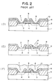
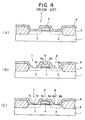
- FIGS.4(A) - (I) show another conventional process of manufacturing a BIC memory cell device.
- these parts constructed identically to those corresponding parts in FIGS.2(A) - (G) are given identical reference numerals and the description thereof will be omitted.
- a step of FIG.4(A) the structure identical to that of the step of FIG.2(A) is formed.
- the holes 7 - 9 are formed through the PSG layer 6 in a step of FIG.4(B).
- the structure is subjected to heat treatment in a step of FIG.4(C).
- the PSG layer 6 causes reflow and then there is formed a thin protective oxide layers 7d, 8d and 9d respectively covering the source region 2, the drain region 3 and the gate electrode 4.
- the sharp edges 7b - 9b at the rim of the holes 7 - 9 are blunted and the inclined walls 7c - 9c surrounding the holes 7 - 9 are formed.
- the protective layer 8d covering the drain region 3 is selectively removed in a step of FIG.4(D).
- the insulator film 10 is deposited uniformly over the surface of the structure of FIG.4(D).
- a step of FIG.4(F) a part of the insulator film 10 is removed except for the part covering the drain region 3, and in a step of FIG.4(G), the protective layers 7d and 9d are removed.
- the wiring conductor layer 11 is deposited. Further, the wiring conductor layer 11 is patterned in a step of FIG.4(I) and the structure similar to that obtained in the process of FIGS.2(A) - (G) is obtained.
- the BIC memory cell device manufactured by such a process still involves a problem of unnecessarily large size due to the blunted shoulder or edge for the holes 7 - 9.
- such a BIC memory cell device is not suited for the integrated circuit memory device comprising numerous BIC memory cell devices particularly when the number of the devices assembled in a unit area of the integrated circuit memory device is enormous.
- this prior art process includes the steps of opening the penetrating hole 7 (FIG.4(B)) through the PSG layer 6, closing the penetrating hole 7 (FIG.4(C)) immediately after it is opened, and again opening the penetrating hole 7 through the PSG layer 6.
- this prior art process involves unnecessarily large number of steps and the manufacturing cost of the device is increased.
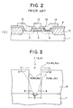
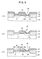
- the BIC memory cell device comprises a substrate 20 similar to the substrate 1 of the prior art on which a source region 21, a drain region 22 and a channel region 20a are defined such that the channel region 20a is located between the source region 21 and the drain region 22.
- the drain region 22 has a so-called lightly doped drain (LDD) structure in which the drain region 22 comprises a lightly doped region 22a having an impurity level of about 1 x 10¹⁸/cm3 and a more heavily doped region having an impurity level of about 1 x 10²⁰/cm3.
- LDD lightly doped drain
- the substrate 20 is doped to a conductive type which is opposite to that of the source and drain regions 21 and 22.
- a gate oxide layer 23a is formed on the substrate in correspondence to the channel region 20a and a gate electrode 23 is deposited on the gate oxide layer 23a.
- a MOS structure T1 there is formed a MOS structure T1 and the structure T1 is separated from adjacent MOS structures by an oxide isolating structure 24 which is similar to the structure 5 of the prior art BIC memory cell device.
- a PSG layer 25 of about 1 ⁇ m in the thickness is deposited on the surface of the MOS structure T1.
- the PSG layer 25 is then removed in a step of FIG.5(B) at a part corresponding to the drain region 22 of the MOS structure T1 by etching.
- the removal of the part of the PSG layer 25 may be made by the usual anisotropic etching such as the reactive ion etching (RIE).
- RIE reactive ion etching
- the entire structure is annealed in a step of FIG.5(C) and the sharp edge 26b is blunted as a result of the reflow of the PSG layer 25 associated with the annealing.
- the annealing is made at a temperature of 950°C - 1050°C for 5 to 10 minutes under a nitrogen atmosphere. Responsive to the annealing, the reflow of the PSG layer 25 occurs and the hole 26 is now defined by the blunted wall 26c. It should be noted that the hole for the source region 21 corresponding to the hole 7 of the prior art is not formed yet in the step of FIG.5(C).
- an insulator film 27 similar to the film 10 of the prior art is deposited on the entire surface of the structure of FIG.5(C) in a step of FIG.5(D).
- the thickness of the insulator film 27 is typically about 50 - 120 ⁇ . Any suitable methods such as sputtering, chemical vapor deposition, heat treatment oxidization or nitridation may be used for the formation of the film 27.
- the insulator film 27 makes a direct contact with the drain region 22 as well as with the blunted wall 26c of the PSG layer 25 which is one of the features of the BIC memory cell device of the present invention.
- a hole 28 is formed through the PSG layer 25 in correspondence to the source region 21 in a step of FIG.5(F).
- This hole 28 is made by the anisotropic etching technique such as RIE and the hole 28 is defined by a straight wall 28a extending perpendicularly to the surface of the substrate 20.
- the hole 28 is defined by a sharp edge 28b.
- the hole 28 does not have a wall such as the wall 26c which increases the diameter towards the top surface of the PSG layer 25.
- a contact hole 29 is opened through the PSG layer 25 in correspondence to the gate electrode 23.
- the hole 28 and the hole 29 are opened simultaneously.
- the hole 29 has a similar corss section as that of the hole 28 and is defined by a straight wall 29a and a sharp rim 29b at the top of the hole 29.
- the wiring conductor layer 30 is deposited on the entire structure in a step of FIG.5(G) and finally the wiring conductor 30 is patterned to wiring electrodes 32, 33 and 34 respectively corresponding to the drain region 22, the source region 21 and the gate electrode 23 as shown in FIG.5(H).
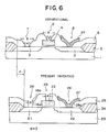
- FIG.6 shows a comparison of the BIC memory cell device of the present invention with the one obtained in the prior art process shown in FIGS.2(A) - (G) or FIGS.4(A) - (H).
- FIGS.2(A) - (G) or FIGS.4(A) - (H) For the sake of simplicity, only essential parts of the structure are illustrated. In the drawing, these parts constructed identically to those corresponding parts in the preceding drawings are given identical reference numerals and the description thereof will be omitted.
- a diameter D of the hole 7 or 9 of the prior art BIC memory is reduced to a diameter d which is substantially smaller than the diameter D for the holes 28 and 29 of the device of the present invention.
- the size of the BIC memory cell device of the present invention is reduced by a distance ⁇ as compared to the conventional device.
- the present structure is particularly effective in reducing the size of the MOS transistor T1 when the transistor is formed by an extremely fine patterning. For example, when the gate electrode extends for about 0.5 ⁇ m between the source region 21 and the drain region 22, a cell size reduction of up to 25 % can be achieved.
- FIGS.5(A) - (H) does not involve the step corresponding to the step of FIG.4(C) and the step of FIG.4(G) of the prior art manufacturing process and therefore the manufacturing process of the present invention is simplified as compared to the prior art process of FIGS.4(A) - (I).
- the etching process used for opening the hole 26 in the step of FIG.5(B) is not limited to the reactive ion etching, but an isotropic etching process such as the wet etching using a hydrofluoric acid (HF) solution and an ammonium fluoride buffer solution, or a combination of the reactive ion etching and the isotropic etching may be used as well.
- an isotropic etching process such as the wet etching using a hydrofluoric acid (HF) solution and an ammonium fluoride buffer solution, or a combination of the reactive ion etching and the isotropic etching may be used as well.
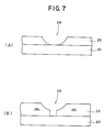
- the isotropic etching is used, the hole 26 formed through the PSG layer 25 has a cross section which is substantially blunted from the beginning as shown in FIG.7(A). In this case the step of annealing shown in FIG.5(C) can be omitted and the manufacturing process can be simplified.
- the material for the insulator layer 25 is not limited to the phospho-silicate glass having a low melting point but a material having a high melting point such as a silica glass deposited by CVD process, for example, may be used for the insulator layer 25.
- FIG.7(B) is an example of the cross section of the hole 26 opened by a combination of the isotropic etching process and the RIE process. In this process, a first part 261 of the hole 26 is formed by the isotropic etching and then a second part 262 is formed by the RIE. Both of the cross sections of the hole 26 of FIGS.7(A) and (B) are effective in preventing the premature breakdown of the insulator film 27 deposited thereon.
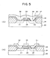
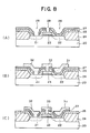
- FIGS.8(A) - (C) show another embodiment of the manufacturing process of the present invention and the structure obtained as a result of the manufacturing process.
- these parts constructed identically to those corresponding parts in the preceding drawings are given identical reference numerals and the description thereof will be omitted.
- the holes 28 and 29 are formed in the structure obtained in the step of FIG.5(D) directly through the PSG layer 25 and the insulator film 27.
- the holes 28 and 29 are formed so as to penetrate through the PSG layer 25 and the insulator film 27 deposited thereon.
- the wiring electrodes 31, 32 and 33 are formed as illustrated in FIG.8(B). The intervening steps of depositing the wiring conductor layer 30 and patterning the layer 30 thus deposited are omitted for the sake of simplicity.
- a part of the insulator film 27 is removed except for those sandwiched between the PSG layer 25 and the wiring electrodes 31, 32 or 33 in a step of FIG.8(C).
- the BIC memory cell device having a structure thus obtained has the insulator film 27 between the wiring electrode 31 and the PSG layer 25 but functions similarly to the BIC memory cell device obtained in the process of FIGS.5(A) - (H). Further, one may eliminate the step of the FIG.8(C). In this case, the surface of the BIC memory cell device is protected against moisture by the insulator film 27 and the manufacturing process is simplified at the same time.
- FIGS.9(A) and (B) show another embodiment of the manufacturing process of the present invention.
- these parts constructed identically to those corresponding parts in the preceding drawings are given identical reference numerals and the description thereof will be omitted.
- a protective layer 34 such as a thin polysilicon layer is deposited on the insulator film 27 after the film 27 is deposited on the PSG layer 25.
- a protective layer 34 protects the insulator film 27 when the surface of the insulator film 27 is prepared for the deposition of the wiring electrode 31 by etching. Such an etching is made in order to obtain a fresh surface for the insulator film 27 as well as for the PSG layer 25.
- the thickness of the insulator film 27 is extremely small (50 - 120 ⁇ ), there is a substantial risk that the insulator film 27 is excessively removed by the etching.
- the excessive etching of the insulator film 27 is prevented by the polysilicon protective layer 34.
- the layer 34 may be a pure polysilicon when the thickness of the polysilicon protective layer 34 is in the order of about 500 ⁇ .
- a doped polysilicon is used in order to secure an excellent electrical conductivity in the protective layer 34.
- FIG.9(A) is obtained by simply depositing the protective layer 34 on the insulator film 27 after the step of FIG.5(D) and thereafter performing the process of FIGS.5(E) -(H), while the structure of FIG.9(B) is obtained by performing the process of FIGS.8(A) - (C) after the deposition of the layer 34.
Landscapes
- Semiconductor Memories (AREA)
- Read Only Memory (AREA)
- Dram (AREA)
Applications Claiming Priority (4)
| Application Number | Priority Date | Filing Date | Title |
|---|---|---|---|
| JP8274788 | 1988-04-04 | ||
| JP82746/88 | 1988-04-04 | ||
| JP82747/88 | 1988-04-04 | ||
| JP63082746A JPH01253959A (ja) | 1988-04-04 | 1988-04-04 | 半導体装置の製造方法 |
Publications (3)
| Publication Number | Publication Date |
|---|---|
| EP0336679A2 true EP0336679A2 (de) | 1989-10-11 |
| EP0336679A3 EP0336679A3 (de) | 1991-09-25 |
| EP0336679B1 EP0336679B1 (de) | 1994-06-01 |
Family
ID=26423762
Family Applications (1)
| Application Number | Title | Priority Date | Filing Date |
|---|---|---|---|
| EP89303271A Expired - Lifetime EP0336679B1 (de) | 1988-04-04 | 1989-04-03 | BIC-Speicherzellenstruktur und Herstellungsverfahren dafür |
Country Status (5)
| Country | Link |
|---|---|
| US (1) | US5075249A (de) |
| EP (1) | EP0336679B1 (de) |
| JP (1) | JP2506183B2 (de) |
| KR (1) | KR920005323B1 (de) |
| DE (1) | DE68915603T2 (de) |
Cited By (1)
| Publication number | Priority date | Publication date | Assignee | Title |
|---|---|---|---|---|
| EP0510604A3 (de) * | 1991-04-23 | 2001-05-09 | Canon Kabushiki Kaisha | Halbleiteranordnung und Verfahren zu ihrer Herstellung |
Families Citing this family (11)
| Publication number | Priority date | Publication date | Assignee | Title |
|---|---|---|---|---|
| US5234853A (en) * | 1990-03-05 | 1993-08-10 | Fujitsu Limited | Method of producing a high voltage MOS transistor |
| US5404029A (en) * | 1990-04-12 | 1995-04-04 | Actel Corporation | Electrically programmable antifuse element |
| EP0509631A1 (de) * | 1991-04-18 | 1992-10-21 | Actel Corporation | Antischmelzsicherungen mit minimalischen Oberflächen |
| US5581111A (en) * | 1993-07-07 | 1996-12-03 | Actel Corporation | Dielectric-polysilicon-dielectric antifuse for field programmable logic applications |
| TW287313B (de) * | 1995-02-20 | 1996-10-01 | Matsushita Electric Industrial Co Ltd | |
| US5888858A (en) | 1996-01-20 | 1999-03-30 | Semiconductor Energy Laboratory Co., Ltd. | Semiconductor device and fabrication method thereof |
| US5909049A (en) * | 1997-02-11 | 1999-06-01 | Actel Corporation | Antifuse programmed PROM cell |
| US5968851A (en) * | 1997-03-19 | 1999-10-19 | Cypress Semiconductor Corp. | Controlled isotropic etch process and method of forming an opening in a dielectric layer |
| US6700151B2 (en) * | 2001-10-17 | 2004-03-02 | Kilopass Technologies, Inc. | Reprogrammable non-volatile memory using a breakdown phenomena in an ultra-thin dielectric |
| US10090360B2 (en) | 2015-02-13 | 2018-10-02 | Taiwan Semiconductor Manufacturing Co., Ltd. | Method of manufacturing a semiconductor structure including a plurality of trenches |
| CN108470676A (zh) * | 2018-04-04 | 2018-08-31 | 睿力集成电路有限公司 | 击穿式电熔丝结构及其形成方法、半导体器件 |
Family Cites Families (12)
| Publication number | Priority date | Publication date | Assignee | Title |
|---|---|---|---|---|
| US3969150A (en) * | 1973-12-03 | 1976-07-13 | Fairchild Camera And Instrument Corporation | Method of MOS transistor manufacture |
| US4288256A (en) * | 1977-12-23 | 1981-09-08 | International Business Machines Corporation | Method of making FET containing stacked gates |
| US4282647A (en) * | 1978-04-04 | 1981-08-11 | Standard Microsystems Corporation | Method of fabricating high density refractory metal gate MOS integrated circuits utilizing the gate as a selective diffusion and oxidation mask |
| US4442591A (en) * | 1982-02-01 | 1984-04-17 | Texas Instruments Incorporated | High-voltage CMOS process |
| US4453325A (en) * | 1982-06-24 | 1984-06-12 | Ofsowitz Warwick N | Advertising display means for parking meter and the like |
| US4388147A (en) * | 1982-08-16 | 1983-06-14 | Intel Corporation | Method for steam leaching phosphorus from phosphosilicate glass during semiconductor fabrication |
| US4498224A (en) * | 1982-12-23 | 1985-02-12 | Tokyo Shibaura Denki Kabushiki Kaisha | Method of manufacturing a MOSFET using accelerated ions to form an amorphous region |
| JPH0693494B2 (ja) * | 1984-03-16 | 1994-11-16 | 株式会社日立製作所 | 半導体集積回路装置の製造方法 |
| JPH073855B2 (ja) * | 1985-07-26 | 1995-01-18 | 富士通株式会社 | 半導体装置の製造方法 |
| JPS62128557A (ja) * | 1985-11-29 | 1987-06-10 | Fujitsu Ltd | 半導体記憶装置とその書込み方法 |
| JPS62128556A (ja) * | 1985-11-29 | 1987-06-10 | Fujitsu Ltd | 半導体装置 |
| JPS62130525A (ja) * | 1985-11-30 | 1987-06-12 | Fujitsu Ltd | 半導体集積回路の製法 |
-
1989
- 1989-03-31 US US07/331,193 patent/US5075249A/en not_active Expired - Fee Related
- 1989-04-03 DE DE68915603T patent/DE68915603T2/de not_active Expired - Fee Related
- 1989-04-03 JP JP1084611A patent/JP2506183B2/ja not_active Expired - Lifetime
- 1989-04-03 EP EP89303271A patent/EP0336679B1/de not_active Expired - Lifetime
- 1989-04-04 KR KR1019890004459A patent/KR920005323B1/ko not_active Expired
Cited By (2)
| Publication number | Priority date | Publication date | Assignee | Title |
|---|---|---|---|---|
| EP0510604A3 (de) * | 1991-04-23 | 2001-05-09 | Canon Kabushiki Kaisha | Halbleiteranordnung und Verfahren zu ihrer Herstellung |
| US6373099B1 (en) | 1991-04-23 | 2002-04-16 | Canon Kabushiki Kaisha | Method of manufacturing a surrounding gate type MOFSET |
Also Published As
| Publication number | Publication date |
|---|---|
| US5075249A (en) | 1991-12-24 |
| EP0336679A3 (de) | 1991-09-25 |
| DE68915603D1 (de) | 1994-07-07 |
| DE68915603T2 (de) | 1994-09-15 |
| JPH02153566A (ja) | 1990-06-13 |
| KR920005323B1 (ko) | 1992-07-02 |
| KR890016676A (ko) | 1989-11-29 |
| JP2506183B2 (ja) | 1996-06-12 |
| EP0336679B1 (de) | 1994-06-01 |
Similar Documents
| Publication | Publication Date | Title |
|---|---|---|
| US4597060A (en) | EPROM array and method for fabricating | |
| US4937645A (en) | Semiconductor device and a method of manufacturing the same | |
| KR0124149B1 (ko) | 반도체집적회로장치 및 그 제조방법 | |
| JP2787646B2 (ja) | 半導体装置の製造方法 | |
| EP0013508B1 (de) | Halbleiter Vorrichtung und Verfahren zu ihrer Herstellung | |
| US5362662A (en) | Method for producing semiconductor memory device having a planar cell structure | |
| US5500544A (en) | Dynamic random access memory cell and method for fabricating the same | |
| JPH0736437B2 (ja) | 半導体メモリの製造方法 | |
| US5100822A (en) | Semiconductor integrated circuit device and method of production thereof | |
| EP0336679B1 (de) | BIC-Speicherzellenstruktur und Herstellungsverfahren dafür | |
| US5043298A (en) | Process for manufacturing a DRAM cell | |
| US6025227A (en) | Capacitor over bit line structure using a straight bit line shape | |
| US4735915A (en) | Method of manufacturing a semiconductor random access memory element | |
| US4467450A (en) | Random access MOS memory cell using double level polysilicon | |
| US6699776B2 (en) | MOSFET gate insulating film and method of manufacturing the same | |
| US6188099B1 (en) | Storage capacitor structure | |
| US5766995A (en) | Method for forming a DRAM cell with a ragged polysilicon crown-shaped capacitor | |
| US5068698A (en) | MOS semiconductor device having high-capacity stacked capacitor | |
| US5318921A (en) | Method for making a high density ROM or EPROM integrated circuit | |
| US4357747A (en) | Method for producing a semiconductor device having an insulated gate type field effect transistor | |
| GB1600048A (en) | Manufacture of integrated circuits | |
| US5936273A (en) | High-capacitance dynamic random access memory cell having a storage capacitor on a continuous irregular surface | |
| US5940701A (en) | Method for forming a DRAM capacitor with four polysilicon pillars | |
| JP2829012B2 (ja) | 半導体不揮発性記憶装置とその製造方法 | |
| US5160988A (en) | Semiconductor device with composite surface insulator |
Legal Events
| Date | Code | Title | Description |
|---|---|---|---|
| PUAI | Public reference made under article 153(3) epc to a published international application that has entered the european phase |
Free format text: ORIGINAL CODE: 0009012 |
|
| AK | Designated contracting states |
Kind code of ref document: A2 Designated state(s): DE FR GB |
|
| PUAL | Search report despatched |
Free format text: ORIGINAL CODE: 0009013 |
|
| AK | Designated contracting states |
Kind code of ref document: A3 Designated state(s): DE FR GB |
|
| 17P | Request for examination filed |
Effective date: 19920217 |
|
| 17Q | First examination report despatched |
Effective date: 19930818 |
|
| GRAA | (expected) grant |
Free format text: ORIGINAL CODE: 0009210 |
|
| AK | Designated contracting states |
Kind code of ref document: B1 Designated state(s): DE FR GB |
|
| PG25 | Lapsed in a contracting state [announced via postgrant information from national office to epo] |
Ref country code: FR Effective date: 19940601 |
|
| REF | Corresponds to: |
Ref document number: 68915603 Country of ref document: DE Date of ref document: 19940707 |
|
| EN | Fr: translation not filed | ||
| PLBE | No opposition filed within time limit |
Free format text: ORIGINAL CODE: 0009261 |
|
| STAA | Information on the status of an ep patent application or granted ep patent |
Free format text: STATUS: NO OPPOSITION FILED WITHIN TIME LIMIT |
|
| 26N | No opposition filed | ||
| PGFP | Annual fee paid to national office [announced via postgrant information from national office to epo] |
Ref country code: GB Payment date: 19960325 Year of fee payment: 8 |
|
| PGFP | Annual fee paid to national office [announced via postgrant information from national office to epo] |
Ref country code: DE Payment date: 19960418 Year of fee payment: 8 |
|
| PG25 | Lapsed in a contracting state [announced via postgrant information from national office to epo] |
Ref country code: GB Effective date: 19970403 |
|
| GBPC | Gb: european patent ceased through non-payment of renewal fee |
Effective date: 19970403 |
|
| PG25 | Lapsed in a contracting state [announced via postgrant information from national office to epo] |
Ref country code: DE Free format text: LAPSE BECAUSE OF NON-PAYMENT OF DUE FEES Effective date: 19980101 |