EP0334657A2 - Method of surface treatment of copper foil or copper clad laminate for internal layer - Google Patents
Method of surface treatment of copper foil or copper clad laminate for internal layer Download PDFInfo
- Publication number
- EP0334657A2 EP0334657A2 EP89302924A EP89302924A EP0334657A2 EP 0334657 A2 EP0334657 A2 EP 0334657A2 EP 89302924 A EP89302924 A EP 89302924A EP 89302924 A EP89302924 A EP 89302924A EP 0334657 A2 EP0334657 A2 EP 0334657A2
- Authority
- EP
- European Patent Office
- Prior art keywords
- copper
- copper foil
- internal layer
- surface treatment
- treatment
- Prior art date
- Legal status (The legal status is an assumption and is not a legal conclusion. Google has not performed a legal analysis and makes no representation as to the accuracy of the status listed.)
- Granted
Links
Images
Classifications
-
- C—CHEMISTRY; METALLURGY
- C25—ELECTROLYTIC OR ELECTROPHORETIC PROCESSES; APPARATUS THEREFOR
- C25D—PROCESSES FOR THE ELECTROLYTIC OR ELECTROPHORETIC PRODUCTION OF COATINGS; ELECTROFORMING; APPARATUS THEREFOR
- C25D3/00—Electroplating: Baths therefor
- C25D3/02—Electroplating: Baths therefor from solutions
- C25D3/38—Electroplating: Baths therefor from solutions of copper
-
- C—CHEMISTRY; METALLURGY
- C25—ELECTROLYTIC OR ELECTROPHORETIC PROCESSES; APPARATUS THEREFOR
- C25D—PROCESSES FOR THE ELECTROLYTIC OR ELECTROPHORETIC PRODUCTION OF COATINGS; ELECTROFORMING; APPARATUS THEREFOR
- C25D5/00—Electroplating characterised by the process; Pretreatment or after-treatment of workpieces
- C25D5/60—Electroplating characterised by the structure or texture of the layers
- C25D5/605—Surface topography of the layers, e.g. rough, dendritic or nodular layers
-
- H—ELECTRICITY
- H05—ELECTRIC TECHNIQUES NOT OTHERWISE PROVIDED FOR
- H05K—PRINTED CIRCUITS; CASINGS OR CONSTRUCTIONAL DETAILS OF ELECTRIC APPARATUS; MANUFACTURE OF ASSEMBLAGES OF ELECTRICAL COMPONENTS
- H05K3/00—Apparatus or processes for manufacturing printed circuits
- H05K3/38—Improvement of the adhesion between the insulating substrate and the metal
- H05K3/382—Improvement of the adhesion between the insulating substrate and the metal by special treatment of the metal
- H05K3/384—Improvement of the adhesion between the insulating substrate and the metal by special treatment of the metal by plating
-
- H—ELECTRICITY
- H05—ELECTRIC TECHNIQUES NOT OTHERWISE PROVIDED FOR
- H05K—PRINTED CIRCUITS; CASINGS OR CONSTRUCTIONAL DETAILS OF ELECTRIC APPARATUS; MANUFACTURE OF ASSEMBLAGES OF ELECTRICAL COMPONENTS
- H05K2201/00—Indexing scheme relating to printed circuits covered by H05K1/00
- H05K2201/03—Conductive materials
- H05K2201/0332—Structure of the conductor
- H05K2201/0335—Layered conductors or foils
- H05K2201/0355—Metal foils
-
- H—ELECTRICITY
- H05—ELECTRIC TECHNIQUES NOT OTHERWISE PROVIDED FOR
- H05K—PRINTED CIRCUITS; CASINGS OR CONSTRUCTIONAL DETAILS OF ELECTRIC APPARATUS; MANUFACTURE OF ASSEMBLAGES OF ELECTRICAL COMPONENTS
- H05K2203/00—Indexing scheme relating to apparatus or processes for manufacturing printed circuits covered by H05K3/00
- H05K2203/03—Metal processing
- H05K2203/0307—Providing micro- or nanometer scale roughness on a metal surface, e.g. by plating of nodules or dendrites
-
- H—ELECTRICITY
- H05—ELECTRIC TECHNIQUES NOT OTHERWISE PROVIDED FOR
- H05K—PRINTED CIRCUITS; CASINGS OR CONSTRUCTIONAL DETAILS OF ELECTRIC APPARATUS; MANUFACTURE OF ASSEMBLAGES OF ELECTRICAL COMPONENTS
- H05K2203/00—Indexing scheme relating to apparatus or processes for manufacturing printed circuits covered by H05K3/00
- H05K2203/07—Treatments involving liquids, e.g. plating, rinsing
- H05K2203/0703—Plating
- H05K2203/0723—Electroplating, e.g. finish plating
-
- H—ELECTRICITY
- H05—ELECTRIC TECHNIQUES NOT OTHERWISE PROVIDED FOR
- H05K—PRINTED CIRCUITS; CASINGS OR CONSTRUCTIONAL DETAILS OF ELECTRIC APPARATUS; MANUFACTURE OF ASSEMBLAGES OF ELECTRICAL COMPONENTS
- H05K3/00—Apparatus or processes for manufacturing printed circuits
- H05K3/46—Manufacturing multilayer circuits
- H05K3/4611—Manufacturing multilayer circuits by laminating two or more circuit boards
Definitions
- the present invention relates to surface treatment of copper treatment particularly to a method for treating the copper surface of a copper clad laminate used as internal layer circuit inmultilayer printed circuit board and to a method for treating the surface of copper foil for printed circuit boards.
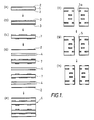
- Fig. 1 shows a process for producing a multilayer printed circuit boards.
- a copper clad laminate is prepared by pressing copper foil (2) on the both sides of a glass-fiber reinforced resin (for example epoxy-resin) (1).
- Fig. (b) rough surface (3) is obtained by being carried out, a surface treatment, that is subject matter of the invention, is conducted to a laminate lined with copper laminated as shown in Fig.1(a).
- a conductor pattern for internal layer is formed.
- the board(6) for internal layer having the thus formed conductor pattern for internal layer foil(2) to form a multilayer board as shown in Fig.1(d).
- holes 5a for through holes are bored, and through hole plating jkis conducted to these holes 5a as shown in Fig.1(g).
- surface pattern is formed by etching.
- 61-13400 after making a copper surface rough chemically by an aqueous solution containing cupric chloride and hydrochloric acid in advance as pretreatment, the surface is immersed into an aqueous solution containing ammonium acetate, cupric acetate, ammonium chloride and aqueous ammonia or an aqueous solution containing trisodium phosphate, sodium hydroxide and sodium chlorite, thereby an oxid film is chemically formed.
- these copper oxide film is substantially poor in acid resistance, particularly very poor in hydrochloric acid resistance.
- a high density multilayer board for surfacemounting wherein a large number of through holes of small size or landless through holes is used, which has come into wide use recently, is immersed into an aqueous solution containing hydrochloric acid which is used for etch back after drilling through holes as multilayer board or for the activation pretreatment of electroless copper plating process the copper oxide film layer as an bonding surface between the resin and copper in the through hole is dissolved with corrosion, that is so-called haloing pink-ring phebinenon, thereby problems such as poor bondability or delaminat ion occur.
- the primary object of the invention is to provide a method of a surface treatment having high acid resistance and sufficient peeling strength without black-oxide treatment as mentioned above. Further, the other objects of the invention are to provide a method of a surface treatment havinng few in the process number and short in the treatment time, and to provide a method of a surface treatment not requiring high temperature treatment.
- the copper surface in treating copper to make a rough surface, for example, in a a copper clad laminate for internal layer, the copper surface is immersed into aqueous diluted sulfuric acid solution to clean the surface after polishing and degreasing as pretreatment. After rinsing , it is immersed into an aqueous solution containing diethylenet riamine pentaacetic acid and copper ion and electrolysis isconducted by using it as a cathode.
- the bath contains diethylenetiamine pentaacetic acid as 10 ⁇ 300 g/l of sodium diethylenetriamine pentaacetate(hereinafter described as DTPA.5Na), more preferably 40 ⁇ 100 g/l, copper ion as 10 ⁇ 100 g/l of cupric sulfate (5 H2O salt), more preferably 30 ⁇ 50 g/l, and its PH is adjusted to 2.5 ⁇ 13.0 by adding sulfuric acid, more preferably 3.5 ⁇ 7.0.
- the weight ratio of DTPA. 5Na/cupric sulfate(5H2O salt) is preferably 0.5 ⁇ 5.0.
- the bath temperature is 30 ⁇ 60°C, more preferably 40 ⁇ 50°C.
- the corrent density is 2 ⁇ 10 A/dm2, thetreatment time is 1 ⁇ 120 seconds, showing 10 ⁇ 500 A.sec/dm2 as quantity of electricity, more preferably 30 ⁇ 100 A.sec/dm2.
- the rough surface formed is extremely minute (below 0.02 ⁇ 0.03 ⁇ m and difficult to obtain satisfactory peelstrength with resin.
- quantity of electricity over 500 A.sec/dm2 the bondability of rough surface itself is obtained, but the rough surface particle is larger (over 1.5 ⁇ 1.9 ⁇ m), thereby it is unfavorable when forming a fine pattern by using aliquid resist.
- copper is preferably used as the anode in electrolysis.
- aminocarboxylic acids such as ethylenediamine tetraacetic acid having molecular structure similar to diethylenetriamine pentaacetic acid are used in place of diethylenetriamine pentaacetic acid, a rough surface good inbondability is not obtained.
- the rough surface is rinsed, dried, and the process for making rough surface is finished.
- the surface may be immersed in an queous solution containing benzotriazol and derivatives thereof to provide rust-resisting property by forming organic film on the surface.
- the surface may be subjected to general chromate treatment such as immersion into aqueous solution of bichromate.
- the copper surface of circuit pattern on the thickness direction of copper clad laminate may be subjected to soft etching by cupric chloride-hydrochloric acid to make rough surface a little, thereby the bondability of surface with resin is elevated.
- the conditions of soft etching in this case are, for example, 20 g/l of cupric chloride (2H2O salt), 300 cc/l of concentrated hydrochloric acid, and at 25°C of bath temperature the surface is subjected to immersion treatment for 30 ⁇ 60 seconds.
- the printed circuit board using copper foil subjected to the above treatment has excellent acid resistance, generating no haloing pink-ring phinomenon and no lowering of peel strength of resin with copper foil. Further, the printed circuit board using copper foil subje cted to the above treatment has excellent heat resistance insoldering without lowering of adhesive strength of solder.
- the above treatment without high temperature treatment process is simple in working and few in process number, reading to low costs.
- the invention has excellent features, contributing to the reliability of a high-multilayer printed circuit board requiring a precise pattern as well as general printed circuit plate.
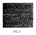
- electrolytic copper foil of 35 ⁇ m in thickness was, after polishing the shiny side, immersed into aqueous 3 % H2SO4 solution at room temperature for 20 seconds, rinsed, and subjected to cathodic electrolysis in theabove-mentioned bath composition under the same conditions. After rinsing and drying, the thus obtained copper rough surface was observed under a scanning electronic microscope, and it was confirmed that the rough surface was composed of uniform fine particle-form of 0.1 ⁇ 0.2 ⁇ m in size.
- the copper foil was laminated with a subsarate of FR-4 grade to examine the peel strength, hydrochloric acid resistance and solder heat resistance. The results are shown in Table 2.
- the copper foil on the external layer was removed by etching to drill a hole of 0.8 mm in diameter, and the laminate was immersed in 20wt% hydrochloric acid for 1 hour, and then whetherhydrochloric acid was soaked into the internal surface or not was judged.
- the results are shown in Table 2.
- electrolytic copper foil of 35 ⁇ m in thickness was, after polishing the shiny side, immersed into aqueous 3% H2SO4 solution at room temperature for 20 seconds, rinsed, and subjected to cathodic electrolysis under the bath composition and conditions shown in Table 1. After rinsing and drying, the copper foil was laminated with a substrate of FR-4 grade to examine the peel strength, hydr ochloric acid resistance and solder heat resistance. The results are shown in Table 2. From the results, the copper rough surface according to the invention is excellent in hydrochloric acid resistance, showing no occurrence of haloing pink-ring phenomenon and no lowering in peel strength after soldering, thereby the method for treating copper surface according to the invention is proved to be highly excellent treatment.
- bonding sheet prepregs were inserted between the both sides and external substrate ( single-sided boards ) and it was laminated by heating to obtain a multilayer laminate (4 layers).
- the copper foil on the external layer was removed by etching to drill a hole of 0.8 mm in diameter, and the laminatewas immersed in 20wt% hydrochloric acid for 1 hour, and then wheher hydrochloric acid was soaked into the internal surfaceor not was judged.
- Table 2 As shown in the results, usual black-oxide treatment shows very poor hydrochloric resistance, generating haloing pink-ring phenomenon.
- electrolytic copper foil of 35 ⁇ m in thickness was, after polishing the glossy surface, immersed into aqueous 3% H2SO4 solution at room temperature for 20 seconds. After rinsing, the copper foil was immersed into the above-mentioned black-oxide treatment bath for 60 seconds. After rinsing and drying, the copper foil was laminated with a substrate of FR-4 grade to examine thepeel strength, hydrochloric acid resistance and solder heat resistance. The results are shown in Table 2. Remarkable lowering of peel strength is shown after soldering, thereby peeling off of layers due to heat shock in soldering may occur, being unreliable and unsuitable for high density circuit.
- the laminate rinsed was immersed into a bath for black-oxide treatment of the following composition for 60 se NaClO2 80 g/ l Na3PO4.12H2O 10 g/ l NaOH 8 g/ l Bath temperature 94°C
- bonding sheet prepregs were inserted between the both sides and external substrate (single-sided boards) and it was laminated by heating to obtain a multilayer laminate (4 layers).
- the copper foil on the external layer was removed by etching to drill a hole of 0.8 mm in diameter, and the laminate was immersed into 20wt% hydrochloric acid for 1 hour,and then whether hydrochloric acid was soaked into the internal layersurface or not was judged. The results are shown in table 2.
- electrolytic copper foil of 35 mm in thickness was, after polishing the shiny side, immersed into aqueous 3% H2SO4 solution at room temperature for 20 seconds. After rinsing, it was treated in a similar manner as above in the above-mentioned cupric chloridehydrochloric acid bath. After rinsing, it was immersed into the above-mentioned black-oxide treatment bath for 60 seconds.
Abstract
Description
- The present invention relates to surface treatment of copper treatment particularly to a method for treating the copper surface of a copper clad laminate used as internal layer circuit inmultilayer printed circuit board and to a method for treating the surface of copper foil for printed circuit boards.
Fig. 1 shows a process for producing a multilayer printed circuit boards. First, as shown in Fig.1(a),a copper clad laminate is prepared by pressing copper foil (2) on the both sides of a glass-fiber reinforced resin (for example epoxy-resin) (1). Next as shown in Fig. (b), rough surface (3) is obtained by being carried out, a surface treatment, that is subject matter of the invention, is conducted to a laminate lined with copper laminated as shown in Fig.1(a). Then, as shown in Fig.1(c), a conductor pattern for internal layer is formed. The board(6) for internal layer having the thus formed conductor pattern for internal layer foil(2) to form a multilayer board as shown in Fig.1(d). Subsequencely, as shown in Fig.1(f),holes 5a for through holes are bored, and through hole plating jkis conducted to theseholes 5a as shown in Fig.1(g). Then, as shown in Fig. 1(h), surface pattern is formed by etching.
In the internal layer materials for multilayer printed circuit boards, to improve the bondability of the copper surface of internal layer circuit with bonding sheet resin prepregs for connecting layers, a method wherein a rough surface composed of copper oxide is formed by immersing the surface into ahigh temperature bath of alkaline chlorite near th boiling point has generally been used, that is called black-oxide (brown-oxide) treatment. For example, as shown in Japanese Patent Publication No. 61-13400, after making a copper surface rough chemically by an aqueous solution containing cupric chloride and hydrochloric acid in advance as pretreatment, the surface is immersed into an aqueous solution containing ammonium acetate, cupric acetate, ammonium chloride and aqueous ammonia or an aqueous solution containing trisodium phosphate, sodium hydroxide and sodium chlorite, thereby an oxid film is chemically formed. - However, these copper oxide film is substantially poor in acid resistance, particularly very poor in hydrochloric acid resistance. When a high density multilayer board for surfacemounting wherein a large number of through holes of small size or landless through holes is used, which has come into wide use recently, is immersed into an aqueous solution containing hydrochloric acid which is used for etch back after drilling through holes as multilayer board or for the activation pretreatment of electroless copper plating process the copper oxide film layer as an bonding surface between the resin and copper in the through hole is dissolved with corrosion, that is so-called haloing pink-ring phebinenon, thereby problems such as poor bondability or delaminat ion occur.
- To improve such defects, for examle, a method wherein the chemical resistance of copper surface is improved by electrolytic reduction of copper oxide film prepared in advance in Japanese Patent Publication No. 50-143689, and a method wherein copper oxide film is reduced by reduced by imidazole-type solution in Japanese Patent Publication No. 60-133794 were proposed.
- However, in any method, the above reducing treatment was reqired to be conducted after usual black-oxide treatment at a high working temperature near the boiling point. Accordingly, these methods had defects that many numbers of processes were necessary, leading to complexity, a strict control of reduction was required, and the finished appearance and rough surface were not uniform.
- The primary object of the invention is to provide a method of a surface treatment having high acid resistance and sufficient peeling strength without black-oxide treatment as mentioned above. Further, the other objects of the invention are to provide a method of a surface treatment havinng few in the process number and short in the treatment time, and to provide a method of a surface treatment not requiring high temperature treatment.
- In the invention, in treating copper to make a rough surface, for example, in a a copper clad laminate for internal layer, the copper surface is immersed into aqueous diluted sulfuric acid solution to clean the surface after polishing and degreasing as pretreatment. After rinsing , it is immersed into an aqueous solution containing diethylenet riamine pentaacetic acid and copper ion and electrolysis isconducted by using it as a cathode.
- The bath contains diethylenetiamine pentaacetic acid as 10∼300 g/ℓ of sodium diethylenetriamine pentaacetate(hereinafter described as DTPA.5Na), more preferably 40∼100 g/ℓ, copper ion as 10∼100 g/ℓ of cupric sulfate (5 H₂O salt), more preferably 30∼50 g/ℓ, and its PH is adjusted to 2.5∼13.0 by adding sulfuric acid, more preferably 3.5 ∼7.0. The weight ratio of DTPA. 5Na/cupric sulfate(5H₂O salt) is preferably 0.5∼5.0. The bath temperature is 30∼60°C, more preferably 40∼50°C. The corrent density is 2 ∼ 10 A/dm², thetreatment time is 1 ∼ 120 seconds, showing 10 ∼500 A.sec/dm² as quantity of electricity, more preferably 30∼100 A.sec/dm². In below 10A.sec/dm2 in quantity of electricity, the rough surface formed is extremely minute (below 0.02 ∼0.03µ m and difficult to obtain satisfactory peelstrength with resin. In quantity of electricity over 500 A.sec/dm², the bondability of rough surface itself is obtained, but the rough surface particle is larger (over 1.5∼1.9 µm), thereby it is unfavorable when forming a fine pattern by using aliquid resist. As the anode in electrolysis, copper is preferably used.
- Even if aminocarboxylic acids such as ethylenediamine tetraacetic acid having molecular structure similar to diethylenetriamine pentaacetic acid are used in place of diethylenetriamine pentaacetic acid, a rough surface good inbondability is not obtained.
- After electrolytic treatment by the above-mentioned method, the rough surface is rinsed, dried, and the process for making rough surface is finished. In the case of long-term storage of the rough surface until the circuit pattern forming process, that is the next process, or in the case of copper foil for printed circuit boards, the surface may be immersed in an queous solution containing benzotriazol and derivatives thereof to provide rust-resisting property by forming organic film on the surface. The surface may be subjected to general chromate treatment such as immersion into aqueous solution of bichromate.
- Before peeling off etching regist after forming circuit pattern, the copper surface of circuit pattern on the thickness direction of copper clad laminate may be subjected to soft etching by cupric chloride-hydrochloric acid to make rough surface a little, thereby the bondability of surface with resin is elevated. The conditions of soft etching in this case are, for example, 20 g/ℓ of cupric chloride (2H₂O salt), 300 cc/ℓ of concentrated hydrochloric acid, and at 25°C of bath temperature the surface is subjected to immersion treatment for 30 ∼60 seconds.
- By the above-mentioned treatment, as shown in the attached photograph, high density of mucroness of 0.1 ∼0.2 µm in size is formed on the copper surface. Therefore, the printed circuit board using copper foil subjected to the above treatment has excellent acid resistance, generating no haloing pink-ring phinomenon and no lowering of peel strength of resin with copper foil. Further, the printed circuit board using copper foil subje cted to the above treatment has excellent heat resistance insoldering without lowering of adhesive strength of solder. The above treatment without high temperature treatment process is simple in working and few in process number, reading to low costs. Thus, the invention has excellent features, contributing to the reliability of a high-multilayer printed circuit board requiring a precise pattern as well as general printed circuit plate.
-
- Fig.1 (a) ∼ (h) is a typical section of the method for producing multilayer printed circuit plate according to the invention.
- Fig. 2 is the electronic microscopic photograph (15000-fold) of fine copper rough surface obtained in Example 1 by the method according to the invention
- Glass-fiber reinforced epoxy-resin of FR-4 grade and electrolytic copper foil of 35 µm in thickness were laminated by pressing to obtain a double-sided board. After polishing the copper surface, it was immersed into aqueous 3% H₂SO₄ solution at room temperature for 20 seconds. The both sides rinsed were subjected to cathodie electrolysis in a bath of the following composition.
DTPA.5Na 52 g/ℓ Cupric sulfate(5H20 salt) 45 g/ℓ PH (adjusted by sulfuric acid) 4.0 Bath temperature 48°C - At 4 A/dm² of current density for 15 seconds. The both sides were rinsed and dried. Then, bonding sheet prepregs were inserted between the both sides and external substrate (single-sided boards) and the secondary lamination was conducted to obtain a multilayer laminate (4 layers). The copper foil on the external layer was removed by etching to drill a hole of 0.8 mm in diameter and the laminate was immersed in 20wt% hydrochloric acid for 1 hour, and then whether a haloing pink-ring was generated by soaking ofhydrochloric acid into the internal surface or not was judged.
- Separately, electrolytic copper foil of 35 µm in thickness was, after polishing the shiny side, immersed into aqueous 3 % H₂SO₄ solution at room temperature for 20 seconds, rinsed, and subjected to cathodic electrolysis in theabove-mentioned bath composition under the same conditions. After rinsing and drying, the thus obtained copper rough surface was observed under a scanning electronic microscope, and it was confirmed that the rough surface was composed of uniform fine particle-form of 0.1 ∼ 0.2 µm in size. The copper foil was laminated with a subsarate of FR-4 grade to examine the peel strength, hydrochloric acid resistance and solder heat resistance. The results are shown in Table 2.
- Glass-fiber reinforced epoxy-resin of FR-4 grade and electrolytic copper foil of 35µm in thickness were laminated by pressing to obtain a double-sided board. After polishing the copper surface, it was immersed into aqueouss 3% H₂SO₄ solution at room temperature for 20 seconds. The laminate rinsed was subjected to cathodic eletrolysis in a similar manner as Example 1 under the both conditions as shown in Table 1 (P H adjusted by sulfuric acid). After rinsing and drying, bonding sheet prepreg was inserted between the both sides and external substrate (single-sided board) and the secondary lamination was conducted to obtain a multilayer laminate(4 layers). The copper foil on the external layer was removed by etching to drill a hole of 0.8 mm in diameter, and the laminate was immersed in 20wt% hydrochloric acid for 1 hour, and then whetherhydrochloric acid was soaked into the internal surface or not was judged. The results are shown in Table 2.
- Separately, electrolytic copper foil of 35 µm in thickness was, after polishing the shiny side, immersed into aqueous 3% H₂SO₄ solution at room temperature for 20 seconds, rinsed, and subjected to cathodic electrolysis under the bath composition and conditions shown in Table 1. After rinsing and drying, the copper foil was laminated with a substrate of FR-4 grade to examine the peel strength, hydr ochloric acid resistance and solder heat resistance. The results are shown in Table 2. From the results, the copper rough surface according to the invention is excellent in hydrochloric acid resistance, showing no occurrence of haloing pink-ring phenomenon and no lowering in peel strength after soldering, thereby the method for treating copper surface according to the invention is proved to be highly excellent treatment.
- Glass-fiber reinforced epoxy-resin of FR-4 grade and electrolytic copper foil of 35 µm in thickness were laminated by pressing to obtain a double-sided board. After polishing the copper surface, it was immersed into aqueous 3% H₂SO₄ solution at room temperature for 20 seconds. The laminate rinsed was immersed into a bath for black-oxide treatment of the following composition for 60 seconds.
NaClO₂ 60 g/ ℓ Na₃PO₄.12H₂O 10 g/ ℓ NaOH 12 g/ ℓ Bath temperature 98°C - After rinsing and drying, bonding sheet prepregs were inserted between the both sides and external substrate ( single-sided boards ) and it was laminated by heating to obtain a multilayer laminate (4 layers). The copper foil on the external layer was removed by etching to drill a hole of 0.8 mm in diameter, and the laminatewas immersed in 20wt% hydrochloric acid for 1 hour, and then wheher hydrochloric acid was soaked into the internal surfaceor not was judged. The results are shown in Table 2. As shown in the results, usual black-oxide treatment shows very poor hydrochloric resistance, generating haloing pink-ring phenomenon. Separately, electrolytic copper foil of 35 µm in thickness was, after polishing the glossy surface, immersed into aqueous 3% H₂SO₄ solution at room temperature for 20 seconds. After rinsing, the copper foil was immersed into the above-mentioned black-oxide treatment bath for 60 seconds. After rinsing and drying, the copper foil was laminated with a substrate of FR-4 grade to examine thepeel strength, hydrochloric acid resistance and solder heat resistance. The results are shown in Table 2. Remarkable lowering of peel strength is shown after soldering, thereby peeling off of layers due to heat shock in soldering may occur, being unreliable and unsuitable for high density circuit.
- Glass-fiber reinforced epoxy-resin of FR-4 grade and electrolytic copper foil of 35 µm in thickness were molded by pressing to obtain a a double-sided board. After polishing the copper surface, it was immersed into aqueous 3% H₂SO₄ solution at room temperature for 20 seconds. The laminate rinsed was immersed into a bath of the following composition for 30 seconds.
CaCl₂2H₂O 30 g\ℓ HCl(36%) 300 cc/ ℓ Bath temperature 25°C - The laminate rinsed was immersed into a bath for black-oxide treatment of the following composition for 60 se
NaClO₂ 80 g/ ℓ Na₃PO₄.12H₂O 10 g/ ℓ NaOH 8 g/ ℓ Bath temperature 94°C - After rinsing and drying, bonding sheet prepregs were inserted between the both sides and external substrate (single-sided boards) and it was laminated by heating to obtain a multilayer laminate (4 layers). The copper foil on the external layer was removed by etching to drill a hole of 0.8 mm in diameter, and the laminate was immersed into 20wt% hydrochloric acid for 1 hour,and then whether hydrochloric acid was soaked into the internal layersurface or not was judged. The results are shown in table 2.
- Separately, electrolytic copper foil of 35 mm in thickness was, after polishing the shiny side, immersed into aqueous 3% H₂SO₄ solution at room temperature for 20 seconds. After rinsing, it was treated in a similar manner as above in the above-mentioned cupric chloridehydrochloric acid bath. After rinsing, it was immersed into the above-mentioned black-oxide treatment bath for 60 seconds.
- After rinsing and drying the copper foil was laminated into laminate with a substrate of FR-4 grade to examine the peel strength, hydrochloric acid resistance and solder heat resistance. The results are shown in Table 2. The hydroch loric resistance is very poor also in this case, and the remarkable lowering of peel strength is also shown after immersion in solder, being proved to be unreliable.
Table 1 Example NO. Conditions for making rough surface DTPA · 5Na (g/ℓ) CuSO₄ · 5H₂O (g/ℓ) PH Temperature (°C) Current density (A/dm²) Electrolysis time(seconds) 1 52 40 4.0 48 4.0 15 2 60 40 4.5 45 4.0 5 3 50 40 4.5 50 4.0 20 4 80 60 4.5 45 8.0 7 5 50 40 3.5 40 3.0 20 6 60 40 4.5 45 4.0 100 7 70 45 7.0 45 8.0 8 8 150 70 3.9 35 5.0 18 9 20 20 3.8 37 3.0 20 10 72 45 12.0 45 8.0 7 Table 2 Internal layer treatment Haloing pink-ring test *1 Peeling off strength (Kg/cm) *2 normal state after immersion in hydrochoric acid (20wt% HCl 25°C,20 min.) after immersion in solder (250°C, 20 sec,float) Example 1 ○ 1.27 1.25 1.24 2 ○ 1.12 1.10 1.10 3 ○ 1.30 1.30 1.28 4 ○ 1.08 1.05 1.03 5 ○ 1.10 1.07 1.04 6 ○ 1.20 1.17 1.17 7 ○ 1.11 1.10 1.11 8 ○ 1.21 1.20 1.18 9 ○ 1.12 1.12 1.10 10 ○ 1.14 1.12 1.12 Example for comparison 1 × 1.25 0.00 0.75 2 × 1.39 0.00 0.98 *1 ○ ... No soaking of hydrochloric acid × ... Large soaking depth (over 2 mm) *2 Test at 1 mm only in width according to JIS-C-6481
Claims (7)
- (1) A method of the surface of treatment copper foil or a copper clad lalminate for internal layer comprising a step of
cathodic electrolysis of a copper foil or a copper clad laminate for internal layer in an aqueous solution containing diethylenatriamine pentaacetic acid and copper ion. - (2) A method of the surface treatment of copper foil or acopper clad for internal layer as claimed in claim 1. wherein denthylenetriamine pentaacetic acid as sodium diethylenetriamine pentaacetate of 10 ∼300 g/ℓ, and copper ion as cupric sulfate of 10∼100 g/ℓ at the PH of 2.5 ∼13 under the temperature of 30°C∼60°C and quantity of electricity of 10∼500 A.sec/dm².
- (3) A method of the surface treatment of copper foil or a copper clad for internal layer as claimed in claim 1 or 2, wherein the said diethylenetriamine pentaacetic acid in the aqueous solution is sodium diethylenetriamine pentaacetate of 40∼10 g/l.
- (4) A method of the surface treatment of copper foil or a copper clad laminate for internal layer as claimed in claim 1 2, or3, wherein the said copper ion in the aqueous solution is cupric sulfate of 30 ∼50 g/ ℓ.
- (5) A method of the surface treatment of copper foil or a copper clad for internal layer as claimed in claim 1,2,3 or 4 wherein the said temperature is 40∼50°C.
- (6) A method of the surface treatment of copper foil or a copper clad for internal layer as claimed in claim 1,2,3,4, or 5, wherein the said PH is 3.5 ∼7.0.
- (7) A method of the surface treatment of copper foil or a copper clad for internal layer as claimed in claim 1,2,3,4, 5,or 6, wherein the said quantity of electicity is 30∼100 A.sec/dm2.
Applications Claiming Priority (2)
| Application Number | Priority Date | Filing Date | Title |
|---|---|---|---|
| JP63072706A JPH01246393A (en) | 1988-03-25 | 1988-03-25 | Surface treatment of copper foil for inner layer or copper lined laminated sheet |
| JP72706/88 | 1988-03-25 |
Publications (3)
| Publication Number | Publication Date |
|---|---|
| EP0334657A2 true EP0334657A2 (en) | 1989-09-27 |
| EP0334657A3 EP0334657A3 (en) | 1989-11-15 |
| EP0334657B1 EP0334657B1 (en) | 1994-11-30 |
Family
ID=13497064
Family Applications (1)
| Application Number | Title | Priority Date | Filing Date |
|---|---|---|---|
| EP89302924A Expired - Lifetime EP0334657B1 (en) | 1988-03-25 | 1989-03-23 | Method of surface treatment of copper foil or copper clad laminate for internal layer |
Country Status (4)
| Country | Link |
|---|---|
| US (1) | US4981560A (en) |
| EP (1) | EP0334657B1 (en) |
| JP (1) | JPH01246393A (en) |
| DE (1) | DE68919498T2 (en) |
Cited By (2)
| Publication number | Priority date | Publication date | Assignee | Title |
|---|---|---|---|---|
| CN110004468A (en) * | 2019-04-20 | 2019-07-12 | 山东金盛源电子材料有限公司 | A kind of compound additive preparing low brittleness electrolytic copper foil |
| KR102190217B1 (en) * | 2019-09-30 | 2020-12-14 | 케이지이티에스(주) | Method for producing high purity cupric oxide for copper plating from electro-copper |
Families Citing this family (23)
| Publication number | Priority date | Publication date | Assignee | Title |
|---|---|---|---|---|
| US5869130A (en) * | 1997-06-12 | 1999-02-09 | Mac Dermid, Incorporated | Process for improving the adhesion of polymeric materials to metal surfaces |
| US6146701A (en) * | 1997-06-12 | 2000-11-14 | Macdermid, Incorporated | Process for improving the adhension of polymeric materials to metal surfaces |
| US6162503A (en) * | 1997-06-12 | 2000-12-19 | Macdermid, Incorporated | Process for improving the adhesion of polymeric materials to metal surfaces |
| US6020029A (en) * | 1997-06-12 | 2000-02-01 | Macdermid, Incorporated | Process for treating metal surfaces |
| US6120639A (en) * | 1997-11-17 | 2000-09-19 | Macdermid, Incorporated | Method for the manufacture of printed circuit boards |
| US6383272B1 (en) | 2000-06-08 | 2002-05-07 | Donald Ferrier | Process for improving the adhesion of polymeric materials to metal surfaces |
| US6419784B1 (en) | 2000-06-21 | 2002-07-16 | Donald Ferrier | Process for improving the adhesion of polymeric materials to metal surfaces |
| US6554948B1 (en) | 2000-08-22 | 2003-04-29 | Donald Ferrier | Process for improving the adhesion of polymeric materials to metal surfaces |
| US20040161545A1 (en) * | 2000-11-28 | 2004-08-19 | Shipley Company, L.L.C. | Adhesion method |
| US6746547B2 (en) | 2002-03-05 | 2004-06-08 | Rd Chemical Company | Methods and compositions for oxide production on copper |
| US7186305B2 (en) * | 2002-11-26 | 2007-03-06 | Donald Ferrier | Process for improving the adhesion of polymeric materials to metal surfaces |
| JP2005206915A (en) * | 2004-01-26 | 2005-08-04 | Fukuda Metal Foil & Powder Co Ltd | Copper foil for printed circuited board, and its production method |
| TWI232710B (en) * | 2004-05-17 | 2005-05-11 | Hannstar Display Corp | Printed circuit board |
| US20060065365A1 (en) * | 2004-09-30 | 2006-03-30 | Ferrier Donald R | Melamine-formaldehyde post-dip composition for improving adhesion of metal to polymer |
| KR20060045208A (en) * | 2004-11-12 | 2006-05-17 | 삼성테크윈 주식회사 | Printed circuit for semi-conductor package and method for manufacturing the same |
| US20070246158A1 (en) * | 2006-04-21 | 2007-10-25 | 3M Innovative Properties Company | Wiring board, production process thereof and connection method using same |
| US7704562B2 (en) * | 2006-08-14 | 2010-04-27 | Cordani Jr John L | Process for improving the adhesion of polymeric materials to metal surfaces |
| US8088246B2 (en) | 2009-01-08 | 2012-01-03 | Cordani Jr John L | Process for improving the adhesion of polymeric materials to metal surfaces |
| US8512504B2 (en) | 2009-05-06 | 2013-08-20 | Steven A. Castaldi | Process for improving adhesion of polymeric materials to metal surfaces |
| US8308893B2 (en) * | 2010-02-01 | 2012-11-13 | Ming De Wang | Nano-oxide process for bonding copper/copper alloy and resin |
| KR101933529B1 (en) * | 2012-12-28 | 2019-03-15 | 동우 화인켐 주식회사 | Etchant composition for copper-containing metal layer and preparing method of an array substrate for liquid crystal display using same |
| KR20150025245A (en) * | 2013-08-28 | 2015-03-10 | 삼성전기주식회사 | Copper clad laminate for printed circuit board and manufacturing method thereof |
| JP6487704B2 (en) * | 2015-02-12 | 2019-03-20 | 福田金属箔粉工業株式会社 | Treated copper foil, copper-clad laminate using the treated copper foil, and printed wiring board |
Citations (1)
| Publication number | Priority date | Publication date | Assignee | Title |
|---|---|---|---|---|
| JPS589996A (en) * | 1981-07-10 | 1983-01-20 | Hitachi Ltd | High-speed copper electroplating solution |
Family Cites Families (5)
| Publication number | Priority date | Publication date | Assignee | Title |
|---|---|---|---|---|
| JPS5529128A (en) * | 1978-08-23 | 1980-03-01 | Mitsui Mining & Smelting Co | Method of surface treating printed circuit copper foil |
| JPS5530818A (en) * | 1978-08-25 | 1980-03-04 | Mitsui Mining & Smelting Co | Method of surface treating printed circuit copper foil |
| JPS60133794A (en) * | 1983-12-21 | 1985-07-16 | 富士通株式会社 | Method of producing multilayer printed board |
| JPS60143689A (en) * | 1983-12-29 | 1985-07-29 | 株式会社日立製作所 | Method of foring circuit on insulating board |
| JPS6113400A (en) * | 1984-06-29 | 1986-01-21 | 株式会社京三製作所 | Monitor control of signal lamp |
-
1988
- 1988-03-25 JP JP63072706A patent/JPH01246393A/en active Granted
-
1989
- 1989-03-23 DE DE68919498T patent/DE68919498T2/en not_active Expired - Fee Related
- 1989-03-23 EP EP89302924A patent/EP0334657B1/en not_active Expired - Lifetime
- 1989-03-23 US US07/327,552 patent/US4981560A/en not_active Expired - Lifetime
Patent Citations (1)
| Publication number | Priority date | Publication date | Assignee | Title |
|---|---|---|---|---|
| JPS589996A (en) * | 1981-07-10 | 1983-01-20 | Hitachi Ltd | High-speed copper electroplating solution |
Non-Patent Citations (2)
| Title |
|---|
| CHEMICAL ABSTRACTS, vol. 69, no. 16, 14th October 1968, page 5982, abstract no. 64051z, Columbus, Ohio, US; N.N. BALASHOVA et al.: "Diethylenetriaminepentaacetic acid electrolyte for copper plating", & ZASHCH. METAL. 1968, 4(2), 213-15 * |
| CHEMICAL ABSTRACTS, vol. 99, no. 6, 8th August 1983, page 449, abstract no. 45439k, Columbus, Ohio, US; & JP-A-58 009 996 (HITACHI LTD) 20-01-1983 * |
Cited By (3)
| Publication number | Priority date | Publication date | Assignee | Title |
|---|---|---|---|---|
| CN110004468A (en) * | 2019-04-20 | 2019-07-12 | 山东金盛源电子材料有限公司 | A kind of compound additive preparing low brittleness electrolytic copper foil |
| CN110004468B (en) * | 2019-04-20 | 2021-03-23 | 山东金盛源电子材料有限公司 | Composite additive for preparing low-brittleness electrolytic copper foil |
| KR102190217B1 (en) * | 2019-09-30 | 2020-12-14 | 케이지이티에스(주) | Method for producing high purity cupric oxide for copper plating from electro-copper |
Also Published As
| Publication number | Publication date |
|---|---|
| EP0334657A3 (en) | 1989-11-15 |
| US4981560A (en) | 1991-01-01 |
| JPH0335394B2 (en) | 1991-05-28 |
| DE68919498D1 (en) | 1995-01-12 |
| DE68919498T2 (en) | 1995-05-18 |
| EP0334657B1 (en) | 1994-11-30 |
| JPH01246393A (en) | 1989-10-02 |
Similar Documents
| Publication | Publication Date | Title |
|---|---|---|
| EP0334657A2 (en) | Method of surface treatment of copper foil or copper clad laminate for internal layer | |
| US5689879A (en) | Metal foil for printed wiring board and production thereof | |
| JP4033611B2 (en) | Copper or copper alloy microetching agent and microetching method using the same | |
| US5800859A (en) | Copper coating of printed circuit boards | |
| EP1667506B1 (en) | Electroless plating process and printed circuit board | |
| CN102046849B (en) | Acid-resistance promoting composition | |
| EP0170414B1 (en) | Process for treating metal surface | |
| US20020070120A1 (en) | Making and using an ultra-thin copper foil | |
| US20050178669A1 (en) | Method of electroplating aluminum | |
| JPS61176192A (en) | Adhesion between copper and resin | |
| US6548153B2 (en) | Composite material used in making printed wiring boards | |
| JP2002292788A (en) | Composite copper foil and method for manufacturing the same | |
| EP1102524A1 (en) | Double-sided printed wiring board and method for manufacturing multilayer printed wiring board having three or more layers | |
| US6319620B1 (en) | Making and using an ultra-thin copper foil | |
| EP0460856B1 (en) | Copper foil for inner layer circuit of multi-layered printed circuit board, method of producing the same and multi-layered printed circuit board having the same | |
| US5538616A (en) | Process for copper plating a wiring board | |
| US7037597B2 (en) | Copper foil for printed-wiring board | |
| US6632344B1 (en) | Conductive oxide coating process | |
| JP2755058B2 (en) | Metal foil for printed wiring board, method of manufacturing the same, and method of manufacturing wiring board using the metal foil | |
| JP2002060967A (en) | Surface treating method for copper or copper alloy | |
| US6579568B2 (en) | Copper foil for printed wiring board having excellent chemical resistance and heat resistance | |
| EP0996318B1 (en) | Novel composite foil, process for producing the same and copper-clad laminate | |
| JP3615973B2 (en) | Novel composite foil and manufacturing method thereof, copper-clad laminate | |
| JP3185516B2 (en) | Method for manufacturing multilayer wiring board | |
| JP6304829B2 (en) | Copper foil for laser processing, copper foil for laser processing with carrier foil, copper-clad laminate, and method for producing printed wiring board |
Legal Events
| Date | Code | Title | Description |
|---|---|---|---|
| PUAI | Public reference made under article 153(3) epc to a published international application that has entered the european phase |
Free format text: ORIGINAL CODE: 0009012 |
|
| PUAL | Search report despatched |
Free format text: ORIGINAL CODE: 0009013 |
|
| 17P | Request for examination filed |
Effective date: 19890414 |
|
| AK | Designated contracting states |
Kind code of ref document: A2 Designated state(s): DE GB |
|
| RHK1 | Main classification (correction) |
Ipc: C25D 3/38 |
|
| AK | Designated contracting states |
Kind code of ref document: A3 Designated state(s): DE GB |
|
| 17Q | First examination report despatched |
Effective date: 19910821 |
|
| GRAA | (expected) grant |
Free format text: ORIGINAL CODE: 0009210 |
|
| AK | Designated contracting states |
Kind code of ref document: B1 Designated state(s): DE GB |
|
| REF | Corresponds to: |
Ref document number: 68919498 Country of ref document: DE Date of ref document: 19950112 |
|
| PLBE | No opposition filed within time limit |
Free format text: ORIGINAL CODE: 0009261 |
|
| STAA | Information on the status of an ep patent application or granted ep patent |
Free format text: STATUS: NO OPPOSITION FILED WITHIN TIME LIMIT |
|
| 26N | No opposition filed | ||
| REG | Reference to a national code |
Ref country code: GB Ref legal event code: IF02 |
|
| PGFP | Annual fee paid to national office [announced via postgrant information from national office to epo] |
Ref country code: GB Payment date: 20040113 Year of fee payment: 16 |
|
| PGFP | Annual fee paid to national office [announced via postgrant information from national office to epo] |
Ref country code: DE Payment date: 20040329 Year of fee payment: 16 |
|
| PG25 | Lapsed in a contracting state [announced via postgrant information from national office to epo] |
Ref country code: GB Free format text: LAPSE BECAUSE OF NON-PAYMENT OF DUE FEES Effective date: 20050323 |
|
| PG25 | Lapsed in a contracting state [announced via postgrant information from national office to epo] |
Ref country code: DE Free format text: LAPSE BECAUSE OF NON-PAYMENT OF DUE FEES Effective date: 20051001 |
|
| GBPC | Gb: european patent ceased through non-payment of renewal fee |
Effective date: 20050323 |