EP0334334B1 - Photo-cathode image projection apparatus for patterning a semiconductor device - Google Patents
Photo-cathode image projection apparatus for patterning a semiconductor device Download PDFInfo
- Publication number
- EP0334334B1 EP0334334B1 EP89105166A EP89105166A EP0334334B1 EP 0334334 B1 EP0334334 B1 EP 0334334B1 EP 89105166 A EP89105166 A EP 89105166A EP 89105166 A EP89105166 A EP 89105166A EP 0334334 B1 EP0334334 B1 EP 0334334B1
- Authority
- EP
- European Patent Office
- Prior art keywords
- photoelectron
- mask
- wafer
- stage
- photo
- Prior art date
- Legal status (The legal status is an assumption and is not a legal conclusion. Google has not performed a legal analysis and makes no representation as to the accuracy of the status listed.)
- Expired - Lifetime
Links
Images


Classifications
-
- H—ELECTRICITY
- H01—ELECTRIC ELEMENTS
- H01L—SEMICONDUCTOR DEVICES NOT COVERED BY CLASS H10
- H01L21/00—Processes or apparatus adapted for the manufacture or treatment of semiconductor or solid state devices or of parts thereof
- H01L21/02—Manufacture or treatment of semiconductor devices or of parts thereof
- H01L21/04—Manufacture or treatment of semiconductor devices or of parts thereof the devices having at least one potential-jump barrier or surface barrier, e.g. PN junction, depletion layer or carrier concentration layer
- H01L21/18—Manufacture or treatment of semiconductor devices or of parts thereof the devices having at least one potential-jump barrier or surface barrier, e.g. PN junction, depletion layer or carrier concentration layer the devices having semiconductor bodies comprising elements of Group IV of the Periodic System or AIIIBV compounds with or without impurities, e.g. doping materials
- H01L21/30—Treatment of semiconductor bodies using processes or apparatus not provided for in groups H01L21/20 - H01L21/26
-
- B—PERFORMING OPERATIONS; TRANSPORTING
- B82—NANOTECHNOLOGY
- B82Y—SPECIFIC USES OR APPLICATIONS OF NANOSTRUCTURES; MEASUREMENT OR ANALYSIS OF NANOSTRUCTURES; MANUFACTURE OR TREATMENT OF NANOSTRUCTURES
- B82Y10/00—Nanotechnology for information processing, storage or transmission, e.g. quantum computing or single electron logic
-
- B—PERFORMING OPERATIONS; TRANSPORTING
- B82—NANOTECHNOLOGY
- B82Y—SPECIFIC USES OR APPLICATIONS OF NANOSTRUCTURES; MEASUREMENT OR ANALYSIS OF NANOSTRUCTURES; MANUFACTURE OR TREATMENT OF NANOSTRUCTURES
- B82Y40/00—Manufacture or treatment of nanostructures
-
- G—PHYSICS
- G03—PHOTOGRAPHY; CINEMATOGRAPHY; ANALOGOUS TECHNIQUES USING WAVES OTHER THAN OPTICAL WAVES; ELECTROGRAPHY; HOLOGRAPHY
- G03F—PHOTOMECHANICAL PRODUCTION OF TEXTURED OR PATTERNED SURFACES, e.g. FOR PRINTING, FOR PROCESSING OF SEMICONDUCTOR DEVICES; MATERIALS THEREFOR; ORIGINALS THEREFOR; APPARATUS SPECIALLY ADAPTED THEREFOR
- G03F7/00—Photomechanical, e.g. photolithographic, production of textured or patterned surfaces, e.g. printing surfaces; Materials therefor, e.g. comprising photoresists; Apparatus specially adapted therefor
- G03F7/70—Microphotolithographic exposure; Apparatus therefor
- G03F7/70375—Multiphoton lithography or multiphoton photopolymerization; Imaging systems comprising means for converting one type of radiation into another type of radiation
-
- G—PHYSICS
- G03—PHOTOGRAPHY; CINEMATOGRAPHY; ANALOGOUS TECHNIQUES USING WAVES OTHER THAN OPTICAL WAVES; ELECTROGRAPHY; HOLOGRAPHY
- G03F—PHOTOMECHANICAL PRODUCTION OF TEXTURED OR PATTERNED SURFACES, e.g. FOR PRINTING, FOR PROCESSING OF SEMICONDUCTOR DEVICES; MATERIALS THEREFOR; ORIGINALS THEREFOR; APPARATUS SPECIALLY ADAPTED THEREFOR
- G03F7/00—Photomechanical, e.g. photolithographic, production of textured or patterned surfaces, e.g. printing surfaces; Materials therefor, e.g. comprising photoresists; Apparatus specially adapted therefor
- G03F7/70—Microphotolithographic exposure; Apparatus therefor
- G03F7/70691—Handling of masks or workpieces
- G03F7/70716—Stages
- G03F7/70725—Stages control
-
- H—ELECTRICITY
- H01—ELECTRIC ELEMENTS
- H01J—ELECTRIC DISCHARGE TUBES OR DISCHARGE LAMPS
- H01J37/00—Discharge tubes with provision for introducing objects or material to be exposed to the discharge, e.g. for the purpose of examination or processing thereof
- H01J37/30—Electron-beam or ion-beam tubes for localised treatment of objects
- H01J37/317—Electron-beam or ion-beam tubes for localised treatment of objects for changing properties of the objects or for applying thin layers thereon, e.g. for ion implantation
- H01J37/3174—Particle-beam lithography, e.g. electron beam lithography
- H01J37/3175—Projection methods, i.e. transfer substantially complete pattern to substrate
-
- H—ELECTRICITY
- H01—ELECTRIC ELEMENTS
- H01J—ELECTRIC DISCHARGE TUBES OR DISCHARGE LAMPS
- H01J2237/00—Discharge tubes exposing object to beam, e.g. for analysis treatment, etching, imaging
- H01J2237/02—Details
- H01J2237/0203—Protection arrangements
- H01J2237/0206—Extinguishing, preventing or controlling unwanted discharges
-
- H—ELECTRICITY
- H01—ELECTRIC ELEMENTS
- H01J—ELECTRIC DISCHARGE TUBES OR DISCHARGE LAMPS
- H01J2237/00—Discharge tubes exposing object to beam, e.g. for analysis treatment, etching, imaging
- H01J2237/02—Details
- H01J2237/026—Shields
- H01J2237/0262—Shields electrostatic
-
- H—ELECTRICITY
- H01—ELECTRIC ELEMENTS
- H01J—ELECTRIC DISCHARGE TUBES OR DISCHARGE LAMPS
- H01J2237/00—Discharge tubes exposing object to beam, e.g. for analysis treatment, etching, imaging
- H01J2237/153—Correcting image defects, e.g. stigmators
-
- H—ELECTRICITY
- H01—ELECTRIC ELEMENTS
- H01J—ELECTRIC DISCHARGE TUBES OR DISCHARGE LAMPS
- H01J2237/00—Discharge tubes exposing object to beam, e.g. for analysis treatment, etching, imaging
- H01J2237/30—Electron or ion beam tubes for processing objects
- H01J2237/303—Electron or ion optical systems
-
- H—ELECTRICITY
- H01—ELECTRIC ELEMENTS
- H01J—ELECTRIC DISCHARGE TUBES OR DISCHARGE LAMPS
- H01J2237/00—Discharge tubes exposing object to beam, e.g. for analysis treatment, etching, imaging
- H01J2237/30—Electron or ion beam tubes for processing objects
- H01J2237/304—Controlling tubes
- H01J2237/30455—Correction during exposure
-
- H—ELECTRICITY
- H01—ELECTRIC ELEMENTS
- H01J—ELECTRIC DISCHARGE TUBES OR DISCHARGE LAMPS
- H01J2237/00—Discharge tubes exposing object to beam, e.g. for analysis treatment, etching, imaging
- H01J2237/30—Electron or ion beam tubes for processing objects
- H01J2237/317—Processing objects on a microscale
- H01J2237/3175—Lithography
- H01J2237/31777—Lithography by projection
- H01J2237/31779—Lithography by projection from patterned photocathode
Definitions
- the present invention generally relates to fabrication of integrated circuits, and more particularly to a photo-cathode image projection apparatus according to the first part of claim 1 and a method of exposing an object to a photoelectron beam according to the first part of claim 15, used for patterning a semiconductor device in fabrication of an integrated circuit.
- VLSI very large scale integrated circuit
- an extremely fine patterning is required so as to provide as many semiconductor devices as possible in a unit area.
- a photolithography technique using ultraviolet radiation is used for this purpose. Responsive to the ultraviolet irradiation, an optical image of a desired device is focused on a photoresist deposited on a wafer or substrate through a suitable mask, and the photoresist is thus exposed to the ultraviolet irradiation in accordance with the desired pattern of the semiconductor device.
- Such a patterning using the ultraviolet light or other visible and invisible lights has a basic limitation in that the minimum thickness of a line possible to be attained in the patterning is limited due to the relatively large wavelength of the light which is typically in the order of 400 nm (4000A).
- various techniques are developed using other type of radiations. Among others, electron beam lithography using an electron beam as the radiation, X-ray beam lithography using an X-ray beam as the radiation, and photo-cathode image projection technique using a photoelectron emitted responsive to an irradiation of a suitable material by an optical beam as the radiation, are widely studied.
- an electron beam having a circular or rectangular cross section is used for exposing the photoresist.
- the electron beam is deflected and moved over the surface of the wafer according to a predetermined pattern.
- the wafer itself is moved.
- a column system including electromagnetic lens and acceleration system is used for focusing, shaping and deflection of the electron beam.
- a stage system is used for supporting and moving the wafer to a direction so that a desired image of pattern is written on the wafer in cooperation with the movement of the electron beam. Using a suitable acceleration voltage, a very fine image of pattern can be written without using mask.
- the X-ray beam lithography is a proximity printing technique in which the mask and the photoresist are separated by a minute gap, and an X-ray having a wavelength in the order of 0,1 - 1 nm (1 - 10 A) is used for the irradiation.
- This technique though capable of providing an improved resolution as compared to the conventional photolithography technique, has a problem in that a bulky X-ray generator has to be used for the X-ray source. Further, there is a problem in that the wafer, X-ray source and the mask has to be aligned with an extremely high precision. For this purpose, a specially designed aligner has to be used.
- the gap between the mask and the wafer is changed from a nominal or designed value particularly when the diameter of the wafer is increased.
- the gap between the mask and a wafer surface across the gap tends to be changed in one position and the other due to the deformation of the mask or non-flat surface of the wafer.
- Such a change in the gap results in a blur in the image of pattern on the wafer.
- the material which can be used for the mask is limited as such a mask has to absorb the X-ray.
- the intensity of the X-ray beam obtained from the commonly available X-ray generator is usually not sufficient for an efficient patterning operation.
- the throughput achieved by the X-ray beam lithography is too small for mass production of integrated circuits.
- SOR synchrotron orbit radiation ring
- the photo-cathode image projection technique is advantageous as it provides a high resolution comparable to that of the electron beam lithography in combination with a high throughput comparable to that of the photolithography.
- a material for emitting a photoelectron when irradiated by a light and another material not emitting electron are patterned on a mask according to the desired pattern, and the photoelectron emitted from the mask is focused on the surface of the wafer which is coated with the photoresist.
- the photoelectron emitted from the mask is accelerated and focused by magnetic and electric fields established between the mask and the wafer, and an image of a semiconductor pattern corresponding to the pattern formed on the mask is transferred to the photoresist covering the surface of the wafer.
- a typical photo-cathode image projection apparatus comprises a mask such as the one already described, a stage for supporting the wafer deposited with the photoresist, focusing coil for focusing the photoelectron on the wafer, a high voltage source which applies a high voltage between the mask and the stage for acceleration of the photoelectron, and an evacuated chamber for accommodating the mask and the stage.
- Another object of the present invention is to provide a photo-cathode image projection apparatus for focusing a photoelectron emitted from a mask patterned with a material which releases the photoelectron responsive to an optical irradiation, on a surface of a wafer held on a stage, wherein a screening electrode plate having a slit therein for passing the photoelectron is disposed between the mask and the stage in a state such that the electrode plate and the stage are in a same electrical potential level.
- electrical discharge between the wafer and the mask due to a high acceleration voltage between the wafer and mask is eliminated by the screening electrode plate and the risk that the pattern on the mask being damaged by the scattering of the photoresist is substantially reduced.
- Another object of the present invention is to provide a method of patterning a semiconductor device on a semiconductor wafer by irradiating a surface of the semiconductor wafer by a photoelectron beam emitted from a photoelectron mask patterned with a material which releases the photoelectron responsive to an optical irradiation, wherein the photoelectron beam is shaped to have a thin linear cross section extending in a first direction in correspondence to a linear portion in said photoelectron mask.
- the linear portion of the mask extending in said first direction and thus corresponding to the portion of the mask where the photoelectron beam is produced responsive to the optical irradiation, is moved across the mask in a direction perpendicular to the elongating direction during exposure of the wafer by moving the optical irradiation relative to the photoelectron mask, and responsive thereto, the photoelectron beam is moved in the second direction. Further, the wafer is moved parallel to said second direction with a predetermined relative speed to the speed of movement of the photoelectron beam.
- the image of entire pattern of the semiconductor device is projected on the semiconductor wafer through a thin slit in an electrode plate which shields the semiconductor wafer from an electrical field of the photoelectron mask without causing electrical discharge between the photoelectron mask and the wafer. Further, the image of the pattern of the semiconductor device is expanded or compressed as desired in said second direction by changing the relative speed of the movement of the beam and the wafer.
- Another object of the present invention is to provide a photo-cathode image projection apparatus for focusing a photoelectron emitted from a mask which is applied with a high acceleration voltage and patterned with a material which releases the photoelectron responsive to an irradiation of light, on a surface of a wafer held on a stage through a screening electrode plate held at an electrical potential level which is identical to that of the stage and having a slit for passing a part of the photoelectron emitted from the mask, wherein additional electrode means is provided between the stage and the electrode plate for correcting a path of the photoelectron reaching the wafer.
- Still another object of the present invention is to provide a photo-cathode image projection apparatus for focusing a photoelectron emitted from a mask patterned according to a desired pattern by a material which releases the photoelectron responsive to an irradiation of light, on a surface of a wafer held on a stage through a screening electrode disposed between the photoelectron mask and the wafer and having a slit elongating in a first direction thereon, wherein the stage is moved with respect to said screening electrode in a second direction perpendicular to said first direction, and a distortion in an image of the pattern projected on the wafer is corrected by detecting a position of a reference part on the wafer provided in correspondence to a positioning mark on the the mask for positioning purpose.
- the distortion of the image projected on the wafer is automatically corrected, and a continuous exposure of numerous patterns on the wafer is achieved by using such a reference part on the wafer as the positioning reference of the photoelectron beam.
- FIG.1 shows an example of a prior art photo-cathode image projection apparatus.
- a focusing coil 1 creates a parallel magnetic field B extending vertically as illustrated, and a photoelectron mask 2 carrying a pattern to be projected on a semiconductor wafer and a stage 3 for supporting the semiconductor wafer, are disposed perpendicularly to the direction of the magnetic field B in such a state that the mask 2 and the stage 3 face each other.
- the mask 2 is held at a negative electrical potential level with respect to the stage 3 by a d.c. voltage source 11 producing an acceleration voltage so that the photoelectron emitted from the mask 2 is accelerated towards the stage 3.
- a side of the mask 2 which is opposite from the stage 3 is irradiated by a light from a light source 4 producing an ultraviolet light, and responsive to the irradiation, the photoelectron is emitted from the mask from the side which faces the stage 3.
- the electron thus emitted is focused by the focusing coil 1 and further deflected by another coil 5 which is used for proper positioning of the focused electron beam.
- the photoelectron mask comprises a transparent base such as a quartz plate having a thickness of about 500 - 600 f..lm, and is provided with a desired semiconductor pattern by a material 6 such as chromium which absorbs the ultraviolet light. Further, another material 7 which releases photoelectron responsive to irradiation of the ultraviolet light such as cesium iodide or platinum is deposited over the material 4. Further, the stage 3 supports a wafer 8 of a semiconductor material on which a photoresist 9 is deposited.
- a part of the scattered photoresist reaches the mask 2 facing the wafer 8, and the pattern of the material 7 on the mask 2 is covered by such a photoresist.
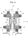
- FIG.2 shows a first embodiment of the photo-cathode image projecting apparatus of the present invention.
- a light source 20 produces an ultraviolet light 20a which is passed through an elongated window 21 and reaches a photoelectron mask 22 supported by a mask stage 23 as a flattened optical beam 20b.
- the photoelectron mask 22 is constructed similarly to the photoelectron mask 2 of the apparatus of FIG.1 and emits a photoelectron beam 22a.
- the photoelectron mask 22 is identical to the mask 2 of FIG.1, the description thereof will not be repeated.
- a semiconductor wafer 24 similar to the wafer 8 is held on a stage 25 and the photoelectron emitted from the photoelectron mask 22 is focused on the surface of the wafer on which is deposited a photoresist (not shown).
- a focusing coil 26 similar to the coil 1 of FIG.1 producing the magnetic field B is used.
- the magnetic field B extends parallel to the general direction of the photoelectron beam.
- a screening electrode 27 between the photoelectron mask 22 and the wafer 24, and the acceleration voltage is applied between the photoelectron mask 22 and the electrode 27.
- the electrode 27 is maintained at the ground potential level and the photoelectron mask 22 is held at a very large negative potential level.
- the electrode 27 is provided with an elongated slit 27a extending parallel to the elongated window 21 and a part of the photoelectron beam 22a passed through this slit 27 reaches the wafer 24 as a flattened electron beam having a thin linear cross section.
- the coil 29 is used for minute adjustment of the image of the pattern projected on the wafer 24 and produces a magnetic field parallel or perpendicular to the magnetic field B.
- the photoelectron mask 22, the electrode 27 and the wafer 24 on the stage 25 are accommodated in an evacuated chamber 30 which is evacuated at an exhaust outlet 31.
- the photoelectron mask 22 is irradiated by the ultraviolet light 20a from the light source 20 at a side opposite from the side which faces the electrode 27. Responsive thereto, the photoelectron is released from the mask 22 according to the pattern of the photoelectron material thereon. The photoelectron is accelerated by the acceleration voltage across the photoelectron mask 22 and the electrode 27 towards the direction of the wafer 24 and reaches the wafer 24 in a form of the electron beam 22a having the linear or elongated cross section after passing through the elongated slit 27a.
- the electrical potential level of the electrode 27 and that of the wafer 24 on the stage 25 are identical.
- the electrical discharge between the wafer 24 and the photoelectron mask 22 is eliminated and the problem of contamination of the photoelectron mask 22 due to the scattering of the photoresist associated with the discharge is eliminated.
- the problem of the unwanted exposure of the photoresist by the back-scattered electron emitted from the wafer 24 is solved as there is no potential gradient between the wafer 24 and the electrode 27.
- the light source 20 may be a mercury-xenon lamp radiating ultraviolet light 20a, and the ultraviolet light 20a is irradiated on the photoelectron mask 22 through the elongated window 21 as already described as the flattened optical beam 20b having the thin linear cross section. Responsive to the irradiation of the photoelectron mask 22, the photoelectron is emitted from the mask 22 and the the photoelectron thus emitted is passed through the elongated slit 27a extending parallel to the elongated window 21 in a form of the photoelectron beam 22a.
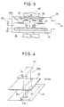
- the size of the window 21 and that of the slit 27a are chosen such that the width and thickness of the linear cross section of the flat optical beam 20b passing through the elongated window 21 is substantially smaller than the width and thickness of the cross section of the flat electron beam 22a passing through the slit 27a.
- the flat optical beam 20b is shaped by the window 21 to have a linear or elongated cross section defined by a width 1 1 and a thickness d 1 (FIG.4) which satisfy a relation and where 1 2 and d 2 respectively specify the width and thickness of the slit 27a as defined in FIG.4.
- the photoelectron beam 22a emitted from the mask 22 and passed through the slit 27a of the electrode 27 is not affected by a local electrical field in a vicinity of an edge of the slit 27a.
- the photoelectron beam 22a passes through the slit 27a at its central part avoiding the vicinity of edge region of the slit 27a and the distortion in the projected image on the wafer 24 due to the disturbed electrical potential at such an edge region is minimized.
- the thickness d 2 of the slit 27a of the electrode 27 is chosen to about 1/10 to 1/20 of a length of a patterned area of the photoelectron mask 22 viewed in the direction of the thickness d 2 .
- This length of the patterned area of the photoelectron mask 22 is of course smaller than the corresponding length of the mask 22 itself.
- the thickness d 2 is chosen larger than the above value, the distortion in the photoelectron beam passed through the slit 27a becomes too conspicuous as a result of leakage in the local electrical field through the slit 27a into the region between the electrode 27 and the stage 25.
- Such a local electrical field is strongly distorted as will be described with reference to other embodiments of the present invention and modifies the path of the photoelectron substantially.
- the thickness d 2 is too small, on the contrary, the efficiency in the patterning is decreased. It is preferred to choose the width 1 2 of the slit 27a of the electrode 27 to about 1.2 times to twice as large as the width of the patterned area of the photoelectron mask 22.
- the position of the light source 20 and the window 21 such that the ultraviolet light 20a radiated form the light source 20 and passed through the window 21 hits the photoelectron mask 22 obliquely.
- the light source 20, the window 21 and the slit 27a are not aligned straight and the unwanted exposure of the photoresist by the ultraviolet light directly reaching to the wafer 24 after passing through the window 21 and the slit 27a is eliminated.
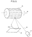
- FIG.5 shows a modification of the light source 20 in which a laser beam 32 produced by a laser 33 is deflected by a rotary polygonal mirror 34 about a rotary axis 35.
- a flat optical beam 20b similar to the optical beam obtained by passing the ultraviolet lig ht 20a through the window 21 is obtained and this optical beam 20b is irradiated on the photoelectron mask 22.
- a second order harmonic of an argon laser having a half-wavelength of 257.25 nm or 244 nm may be used.
- FIG.3 is a modification of the apparatus of FIG.2 in which a permanent magnet 26' is used for producing the magnetic field B.
- a permanent magnet 26' is used for producing the magnetic field B.
- an optical beam 20a' is introduced obliquely from the outside of the chamber 30, as there is provided the permanent magnet 26' behind the photoelectron mask 22 and no space for the path of the light beam 22a is available in this region.
- the optical beam 20a' is reflected by a mirror surface of the electrode 27.
- use of the bulky focusing coil 26 can be omitted and the construction becomes simple.
- FIG.6 shows the overall construction of the apparatus of FIG.2 together with the control part for controlling the various parts of FIG.2.
- these parts constructed identically to those corresponding parts in FIG.2 are given identical reference numerals and the description thereof will be omitted.
- a central processing unit (CPU) 601 cooperates with a magnetic disk memory 602 and a magnetic tape memory 603 for storing a control data and controls the apparatus of FIG.2 via an interface 604.
- the CPU 601 controls the light source 20 and a shutter 36 provided in the path of the optical beam 20b via the interface 604.
- CPU 601 further controls a focusing control system 606 which in turn controls motors 607a and 607b for moving the mask stage 23 and the electrode 27 up and down respectively in a Z direction, a driver 608 for energizing the coil 29, and a driver 609 for applying an acceleration voltage to the mask 22 via the mask stage 23.
- the CPU 601 controls a deflection controller 610 which in turn controls a driver 611 for energizing a magnetic deflector 37 and an electrostatic deflector 38.
- deflectors are provided between the electrode 27 and the stage 25 so as to surround the path of the photoelectron beam 22a and deflects the electron beam in X and Y directions as defined in FIG.6.
- the CPU 601 controls a stage controller 613 which in turn drives a motor 614 for the mask stage 23 and a motor 615 for the stage 25.
- the stage controller 613 drives the motor 614 and 615 responsive to an output of an X-Y position detector 616 which detects the X-Y position of the mask stage 23 and the stage 25.
- the X-Y position detector may be a laser interferometer.
- the light source 20 is turned ON and the shutter 36 is opened. In this state, an operation to achieve an alignment between the mask 22 and the wafer 24 is performed.
- the alignment is made using a back-scattered electron detector 39 which may be a PIN diode disposed on a side of the electrode 27 facing the wafer 24.
- the photoelectron beam 22a is focused on the slit 27a of the electrode 27 by adjusting the position of both or either one of the mask stage 23 or the electrode in the Z direction. Further, the distortion, magnification and the rotation of the image thus formed at the slit 27a is corrected using the coil 29.
- the photoelectron mask 22 and the wafer 24 are moved parallel in an X-Y plane defined by the X and Y axis by moving the corresponding stages 23 and 25.
- the speed of movement of the mask and the wafer is determined on the basis of the sensitivity of the photoresist on the wafer 24 and may be chosen to 10mm/sec, for example. It should be noted that the light source 20 and the electrode 27 are stationary. According to this procedure, the pattern on the photoelectron mask 22 is transferred to the photoresist on the wafer 24 without magnification or compression.
- the speed of movement of the photoelectron mask 22 and the wafer 24 is not necessarily be constant as long as the photoelectron mask and the wafer are moved in a same speed.
- the image projected on the photoresist on the wafer 24 by the photoelectron beam 22a may be compressed to 1/5 of the size of the pattern on the photoelectron mask 22 in the direction of the movement of the mask and the wafer by reducing the speed of movement of the wafer 24 to 1/5 of the moving speed of the photoelectron mask 22.
- the pattern on the photoelectron mask 22 may be such a pattern which is expanded by five times in the direction of movement of the photoelectron mask 22.
- the movement of the photoelectron mask 22 and the wafer 24 is made in synchronization under control of the CPU 601. However, it is inevitable to avoid minute error in the movement of these parts.
- the present apparatus uses the laser interferometer 616 for detection of the position of the mask stage 23 and the stage 25 for the wafer.
- the interferometer 616 produces an output signal indicating the error as aforementioned, and responsive to the output signal, the CPU 601 energizes the electromagnetic deflector 37 and the electrostatic deflector 38 via the deflection controller 610 such that the electron beam is deflected by a minute amount corresponding to the error and the error is compensated.
- the photoelectron beam 22a is deflected in a forward direction to the direction of movement of the mask 22 and the wafer 24 when the moving speed of the mask 22 is relatively slow to the moving speed of the wafer 24.
- the photoelectron beam 22a is deflected in a backward direction to the direction of movement of the mask 22 and the wafer 24.
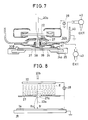
- FIG.7 shows a part of a modification of the apparatus of the present invention in an enlarged scale.
- these parts constructed identically to those corresponding parts of FIG.2 are given identical reference numerals and the description thereof will be omitted.
- a partition wall 40 which divides the chamber 30 into a first chamber region 30A including the photoelectron mask 22 and the electrode 27 and a second chamber region 30B including the stage 25 and the wafer 24.
- the partition wall 40 extends along the electrode 27 and holds a plate 41 on which the magnetic deflector 37, electrostatic deflector 38 and the back-scattered electron detector 39 are carried, between the wall 40 and the wafer 24. Further, the partition wall 40 has an elongated opening 40a in registration with the slit 27a of the electrode 27.
- the photoresist on the wafer 24 is illustrated by a reference numeral 24b and the wafer 24 is fixed on the stage 25 by a wafer holder 24a.
- the chamber region 30A is evacuated by a pump 42 and the chamber region 30B is evacuated by a pump 43 differentially across the wall 40 which extends along the electrode 27.
- the chamber region 30A including the photoelectron mask 22 and the electrode 27 is maintained at a high degree of vacuum such as 133,3 x 10- 8 Pa (10- 8 Torr) irrespective of the existence or non-existence of the wafer 24 on the stage 25.
- the apparatus of the present modification successfully prevents the electrical discharge between the photoelectron mask and the electrode.
- the photoelectron mask 22 and the wafer 24 are moved while the light source 20 and the electrode 27 are stationary.
- the apparatus it is also possible to construct the apparatus such that the light source 20 and the electrode 27 are moved while the photoelectron mask 22 and the stage 25 are held stationary.
- the motor 614 is used to move the light source 20 instead of moving the mask stage 23 and the motor 615 is used to move the electrode 27 instead of moving the stage 24 as indicated in broken line in FIG.6.
- the X-Y position of the light source 20 and the electrode 27 are detected by the interferometer 616 as indicated in the drawing.
- the stage 23 for holding the photoelectron mask 22 to which the high acceleration voltage is applied is held stationary and the design and construction of the apparatus becomes easier, though such an apparatus cannot magnify or compress the image on the wafer 24.
- FIGS.8 -17 a second embodiment of the present invention will be describe width reference to FIGS.8 -17.
- these parts constructed identically to those corresponding parts of the preceding drawings are given identical reference numerals and the description thereof will be omitted.
- the electrical discharge between the photoelectron mask 22 and the wafer 24 on the stage 25 is successfully eliminated as a result of the use of the electrode 27.
- a use of the electrode 27 defined with the slit 27a causes a problem in that the electrical field established by the high acceleration voltage between the photoelectron mask 22 and the electrode 27 is significantly disturbed in the vicinity of the slit 27a.
- FIG.8 shows a typical situation in which a parallel potential surface of the electrical field E is disturbed at the region of the slit 27a and is leaking or invading into the space defined by the electrode 27 and the stage 25.
- FIGS.9(A) and (B) show typical examples of the distortion in the image projected on the photoresist on the wafer 24 in which FIG.9(A) shows various focusing state of the photoelectron beam in the vicinity of the slit 27a and FIG.9(B) shows the distortion corresponding to the focusing state of FIG.9(A) in plan view.
- the projected image not including distortion is represented by a broken line.
- a distortion component represented by a vector is represented by a superposition of magnification of the projected image called "gain component" as represented by a vector and a "rotation component" of the projected image as represented by a vector b respectively.
- the gain component of the distortion represented by the vector a is negative and the image is compressed in a direction perpendicular to the elongating direction of the slit 27a as shown in the case (a).
- the photoelectron beam 22a is focused at a level lower than the plane of the electrode 27, the gain component becomes positive and the projected image on the wafer 24 is magnified as shown in the case (c).
- the gain component of the distortion can be made zero and the magnification of the transferred image on the wafer 24 becomes unity as shown in the case (b) in FIG.9(B).
- the projected image on the wafer 24 has an area identical to the area of the ideal image when the photoelectron beam 22a is focused exactly on the plane of the electrode 27 and then projected on the wafer 24.
- the rotational component b of the distortion does not disappear even when the photoelectron beam 22a is focused exactly on the plane of the electrode 27 as clearly seen in FIG.9(B).
- This rotational component of the distortion is caused as a result of the invasion of the electrical field into the region between the electrode 27 and the wafer 24 as illustrated in FIG.8 and has to be cancelled out using other means than the adjustment of the level of the electrode 27.
- FIG.10 shows a principle of the cancellation of the rotational distortion component of the projected image on the wafer 24 according to a second embodiment of the photo-cathode image projection apparatus of the present invention.
- those parts constructed identically to those corresponding parts of the preceding drawings are given identical reference numerals and the description thereof will be omitted.
- an auxiliary electrode 42 between the electrode 27 and the wafer 24 such that the electrode 42 is movable in the Z-direction along the path of the photoelectron beam 22a.
- the auxiliary electrode 42 comprises a pair of rod shaped electrodes 42a, 42b provided at both sides of the planer photoelectron beam 22a and applied with a suitable correction voltage.
- a suitable correction voltage As a result, there is formed a local electrical field around the electrode 42 and the leakage or invasion of the electrical field into the space between the electrode 27 and the wafer 24 is cancelled by this local electrical field.
- the photoelectron beam 22a is passed through the slit 27a of the electrode 27 as if there is no disturbance in the electrical field.
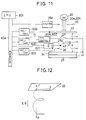
- FIG.11 is a more detailed view of the second embodiment of the present invention.
- these parts constructed identically to those corresponding parts are given identical reference numerals and the description thereof will be omitted.
- the electrode 42 is supplied with a d.c. voltage from a controller 620 and is moved vertically by another controller 621.
- the controllers 620 and 621 are connected to the CPU 601 via the interface 604 and controlled by the CPU 601.
- the auxiliary electrode 42 comprises a pair of rod shaped electrodes 42a, 42b which are separated by a mutual distance of about 1 cm at a level of about 1 cm above the wafer 24.
- the electrode 27 is provided above the electrode 42 with a separation of about 1 cm.
- the electrode 27 in turn is disposed below the photoelectron mask 22 by a distance of about 1cm.
- the auxiliary electrode 42 is provided at a generally mid-position between the electrode 27 and the stage 25 supporting the wafer 24.
- the electron detector 39 for the back-scattered electron is provided not on the electrode 27 as in the example of FIG.6 but is held at a mid-position between the auxiliary electrode 42 and the wafer 24.
- the output of the detector 39 is processed in a processor 622 and is supplied to the CPU 601.
- a particular portion of the wafer 24 provided for positioning purpose is irradiated by the photoelectron beam 20a.
- This particular portion of the wafer may be a small projection or depression formed on a predetermined portion of the wafer 24.
- a photoelectron beam having a small cross section emitted from a particular marking part in the pattern on the mask 22 is used as will be described with reference to the other embodiment of the present invention.
- the back-scattered electron emitted from the wafer 24 responsive to the irradiation of the photoelectron beam is detected by the electron detector 39, and the detector 39 produces an output signal indicating the intensity of the detected back-scattered electron.
- This output of the detector 39 is then processed by the processor 622 and a data indicating the detection of the particular portion of the wafer for the positioning purpose is produced.
- the CPU 601 calculates a deviation in the position of the focused photoelectron beam or beam spot from the expected position of the photoelectron beam estimated from the marking area on the pattern on the mask 22. Further, the CPU 601 controls the photoelectron mask 22, the electrode 27, and the auxiliary electrode 43 via respective controllers such that the predicted position of the beam spot coincides with the actual position of the beam spot of the photoelectron beam used for the positioning.
- auxiliary electrode 42 for correcting the path of the photoelectron beam 22a is provided in the vicinity of the mid-position between the electrode 27 and the wafer 24 as well as the function of the electrode 42 will be described in detail.
- the photoelectron moves in a -Z direction towards the wafer 24 along a spiral orbit.
- the photoelectron undergoes a circular motion in the X-Y plane under the magnetic field B and at the same time moves in the -Z direction under the acceleration by the electrical field E.
- the electron is accelerated in the region between the photoelectron mask 22 and the slit 27a of the electrode 27, but thereafter moves at a constant speed as there is no accelerating electrical field between the electrode 27 and the wafer 24.
- the Z- coordinate of the photoelectron is represented by for the region of uniform acceleration between the photoelectron mask 22 and the slit 27a, and for the region of the constant velocity motion between the slit 27a and the wafer 24.
- v o stands for the initial velocity of the photoelectron in the Z-direction when the photoelectron is emitted from the photoelectron mask 22
- v stands for the velocity of the photoelectron in the Z-direction when the photoelectron passes through the slit 27a.
- the distortion component A of the image of the pattern at the surface of the wafer 24 can be calculated by the following equations: and where f s (z) is a distribution function of the electrical field in the vicinity of the slit 27a, d is a distance between the photoelectron mask and the electrode plate 27, 2d is a distance between the photoelectron mask 22 and the auxiliary electrode 42, and 3d is a distance between the photoelectron mask 22 and the wafer 24.
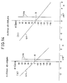
- FIGS.14(A) - (D) show the sine term corresponding to the gain component and cosine term corresponding to the rotation component of the distortion A for various settings of the photo-cathode image projection apparatus in which FIG.14(A) shows the case in which the distance d is chosen to 10 mm and the slit thickness d2 (FIG.4) is chosen to 400 ⁇ m, FIG.14(B) shows the case in which the distance d is chosen to 10mm and the slit thickness d2 is chosen to 500 ⁇ m, FIG.14(C) shows the case in which the distance d is chosen to 10 mm and the slit thickness d2 is chosen to 666 ⁇ m, and FIG.14(D) shows the case in which the distance d is chosen to 10 mm and the slit thickness d2 is chosen to 1000 ⁇ m.
- the ordinate d - C represents the difference in the level between the electrode 27 and the photoelectron mask 22 and the abscissa represents the distortion due to the sine and cosine terms.
- the sine term of the distortion can be eliminated by optimizing the Z-coordinate of the electrode 27 as indicated by arrows A- D.
- the cosine term of the distortion is not. eliminated by such an adjustment.
- the sine term of the distortion A corresponds to the vector a
- the cosine term corresponds to the vector b of the distortion components shown in FIG.9(B).
- the present embodiment uses the auxiliary electrode 42 as shown in FIG.10 which produces an electrical field N2 having a polarity opposite to that of the electrical field N 1 at the level of 2d which is approximately the mid-point between the electrode 27 and the wafer 24.
- a voltage of negative polarity is applied to the auxiliary electrode 42 through the controller 620. It is preferred to construct the electrode 42 by the pair of rod shaped electrodes 42a, 42b disposed in parallel to the slit 27a at both sides of the path of the photoelectron beam 22a as illustrated in FIG.10.
- the electrical field N2 by the auxiliary electrode 42 does not affect the sine term of the distortion A but only affects the cosine term of the distortion and rotates the image projected on the wafer 24.
- Such a modification in the shape of the image by the auxiliary electrode 42 cancels out the rotational distortion component caused by the electrode plate 27.
- the sine term of distortion corresponding to the gain component represented by the vector a in FIG.9 is corrected by adjustment of the level of the electrode 27 and the cosine term of distortion corresponding to the rotational component represented by the vector 1 in FIG.9 is corrected by the auxiliary electrode 42.
- the present embodiment prevents the electrical discharge between the photoelectron mask 22 and the wafer 24.
- the auxiliary electrode 42 is made of a pair of rod shaped electrodes disposed at both sides of the photoelectron beam 22a such that the electrode is movable in the Z-direction by the controller 621.
- the auxiliary electrode 42 is not limited to such an embodiment but may be made of a plurality of electrode pairs as shown in FIG.10 in the solid line and the broken line. Each of the plurality of electrode pairs are applied with a suitable voltage so that the position of the maximum intensity of the electrical field N2 is adjusted. According to this modification, complex mechanism related to the controller 621 for movement of the electrode 42 in the Z-direction can be eliminated and the construction of the apparatus becomes simple.
- auxiliary electrode 42 is not limited to rod-shaped electrodes as illustrated but a flat panel electrode defined with opening for the photoelectron beam may be used similarly.
- electrical voltage applied to the auxiliary electrode 42 is not limited to the negative voltage as illustrated but a positive voltage may be used in combination with the negative voltage. In this case, the photoelectron beam 22a can be deflected uniformly.
- the distortion component obtained for one area of the wafer 24 on which the image is to be projected can be different from the distortion in another area remote from the aforesaid area. It is therefore preferred to correct such a distortion continuously and automatically.
- FIG.15 shows a third embodiment of the present invention wherein the problems aforementioned are eliminated.
- these parts constructed identically to those corresponding parts in the preceding drawings are given identical reference numerals and the description thereof will be omitted.
- the photo-cathode image projection apparatus of the present embodiment comprises a wafer mark detector 630 which detects the deviation in position of the photoelectron beam on the wafer 24 from a predicted position which is defined with respect to a wafer mark provided on the wafer 24 for the positional reference purpose.
- a wafer mark detector 630 which detects the deviation in position of the photoelectron beam on the wafer 24 from a predicted position which is defined with respect to a wafer mark provided on the wafer 24 for the positional reference purpose.
- Examples of the wafer marks can be seen in FIG.16(B) in which the small rectangular projections or depressions designated by aN- 1 -d N- 1 , a N - d N , a N+1 d N+1 , a N+2 , b N+2 ... are the wafer marks.
- the wafer mark detector 630 is supplied with the information indicating the center of these wafer marks from the stage controller 613 for example, and detects the deviation of the photoelectron beam from the center of the wafer mark on the basis of the signal from the back-scattered electron detector 39 indicating the intensity of the back-scattered electron from a region of the wafer including the wafer mark.
- the wafer mark detector 630 then produces a data indicating the deviation of the photoelectron beam from its predicted position and the data thus produced is stored in a memory 601 a cooperating with a processor 601 b.
- the stage controller 613 controls the deflection controller 610 which moves the photoelectron beam to the position corresponding to the wafer mark a N - d N for the detection of the wafer mark.
- the data stored in the wafer mark memory 601 a is then read out by the processor 601 b which may be a part of the CPU 601.
- the processor 601 b in turn controls the focusing controller 606 by supplying a control signal f and the deflection controller 610 by supplying a control signal g and the position of the photoelectron beam on the wafer 24 is moved responsive to the value of the controls signals f and g such that the distortion of the projected image is eliminated.
- FIG.16(A) shows mask marks A - D provided on the photoelectron mask 22 in correspondence to the wafer marks a N - d N . These mask marks are used as the source region for producing the photoelectron beam used to irradiate the wafer marks a N - d N .
- the mask marks A and B are positioned at a front side of an area 22b of the pattern on the photoelectron mask 22 and the mask marks C and D are positioned at a rear side of the area 22b.
- the front side means a side of the area 22b facing the direction in which the photoelectron mask is moved and the rear side is defined as a side of the area 22b opposite to the front side.
- the separation between the mask marks A and B may be made larger than the separation between the mask marks C and D as illustrated in FIG.16(A).
- the wafer 24 is exposed to the photoelectron beam irradiation according to the pattern 22b on the photoelectron mask 22 consecutively, and there is formed a stripe of transferred patterns N-1, N, N+1, ... as illustrated in FIG.16(B).
- the wafer marks are provided such as the wafer marks aN-1 - dN- for the pattern N-1, the wafer marks a N - d N for the pattern N, and the wafer marks a N , l - d N+1 for the pattern N+1.
- FIGS.17(A) and (B) the operation of the photo-cathode image projection apparatus of the present embodiment will be described with reference to FIGS.17(A) and (B).
- these parts constructed identically to those corresponding parts in the preceding drawings are given identical reference numerals and the description thereof will be omitted.
- the optical beam 20b is irradiated on the photoelectron mask 22 while the photoelectron mask 22 and the wafer 24 are moved together in the direction X.
- photoelectron beams 22c and 22d are produced from the mask marks A and B and the photoelectron beams 22c and 22d hit the corresponding wafer marks b N and a N .
- the wafer mark detecting apparatus 630 detects the deviation in position of the photoelectron beams 22c and 22d on the wafer 24 and the position thus obtained is stored in the memory 601 a.
- the photoelectron mask 22 and the wafer 24 are moved in the X-direction at a constant speed, and after a predetermined time, the optical beam 20b irradiates the mask marks C and D as shown in FIG.17(B). Responsive thereto, the photoelectron beams 22c and 22d hit the wafer marks c N and d N , and the deviation in position of the photoelectron beams 22c and 22d is determined by the wafer mark detecting apparatus 630 on the basis of the back-scattered electron emitted from the wafer marks c N and d N . The deviation of the photoelectron beams 22c and 22d thus obtained is stored in the memory 601 a.
- the processor 601 b performs a control of the photoelectron beam for eliminating the stig and dynamic focusing of the photoelectron beam as will be described.
- the processor 601 b controls the focusing controller 606 by the control signal f such that the photoelectron beams 22c and 22d are properly focused on the wafer 24 at the area of the wafer including the wafer marks a N and b N , for example.
- the processor 601 b controls the deflection controller 610 by the control signal g such that the photoelectron beam has a proper square beam spot on the wafer 24 at the same area.
- the processor 601 b stores the value of the control signals f and g for controlling the focusing controller 606 and the deflection controller 610 determined as such.
- the processor repeats the operation described for the area of the wafer 24 including the wafer marks c N and d N and stores the value of the control signals f and g for controlling the focusing controller 606 and the deflection controller 610 determined as such.
- the processor 601 b calculates the value of the controls signals f and g for an arbitrary point x between the wafer marks a N , b N and the wafer marks CN , d N according to an equation: where T(x) stands for the value of the control signals f and g for achieving the proper focusing and shaping of the photoelectron beam 22a on the wafer 24 at a position separated by a distance x from a side or edge of the pattern such as the pattern N on the wafer 24 which is close to the pairs of the wafer marks a N and b N as shown in FIG.16(B), T 1 stands for the magnitude of the control signals to be supplied to the controllers 606 and 610 in order to establish a proper focusing and the proper shaping of
- the equation for interpolation of the controls signals f and g is not limited to such a linear equation but a parabolic equation such as may be used when a number of wafer marks aN-1 - d N- aN - d N , a N+1 . d N+1 , ... are used for correction of the photoelectron beam.
- T 1 for example represents the control signals f and g when the photoelectron beams 22c and 22d hit the part of the wafer 24 including the wafer marks aN- and b N-1 and T 2 represents the control signals f and g when the photoelectron beams 22c and 22d hit the part of the wafer 24 including the wafer marks a N+1 and b N+1 shown in FIG.17(B).
- T 3 represents a parameter obtained by fitting the value of the control signals f and g determined for all of the wafer marks aN-1 - d N- aN - d N , a N+1 - d N+1 , ... by the above second order equation.
- Equation (2) is not limited to the interpolation of the control signals f and g but may be applicable to the correction of the distortion of the image on the wafer 24 represented by the distortion components such as the gain component and the rotational component.
- the distortion of the image further comprises an offset component indicating the translation of the image on the wafer and a trapezoidal distortion component indicating a change in magnification of image within the pattern on the wafer 24.
- each of the four distortion components is obtained for the patterns N-1, N, and N+1 shown in FIG.17(B) using the wafer marks a N-1 - d N- aN- d N , and a N+1 - d N+1 , and the values of the distortion component for these patterns N-1, N and N+1 are fitted according to Equation (2).
- Equation (2) the the distortion of the image on the wafer 24 can be corrected for a wide area such as the area for the patterns N-1, N, N+1, ... with a very high precision.
- FIG.18 shows a modification of the apparatus of FIG.15 in which these parts constructed identically to those corresponding parts are given identical reference numerals and the description thereof will be omitted.
- the focusing coil 26 is replaced by a permanent magnet 26' and the optical beam 20b from the light source 20 is incident to the photoelectron mask 22 obliquely as illustrated.
- Other construction of the apparatus is substantially the same as the apparatus described With reference to FIG.15 and the description thereof will be omitted.
Description
- The present invention generally relates to fabrication of integrated circuits, and more particularly to a photo-cathode image projection apparatus according to the first part of
claim 1 and a method of exposing an object to a photoelectron beam according to the first part of claim 15, used for patterning a semiconductor device in fabrication of an integrated circuit. - In fabrication of a semiconductor integrated circuit including numerous semiconductor devices such as a very large scale integrated circuit (VLSI), an extremely fine patterning is required so as to provide as many semiconductor devices as possible in a unit area. Conventionally, a photolithography technique using ultraviolet radiation is used for this purpose. Responsive to the ultraviolet irradiation, an optical image of a desired device is focused on a photoresist deposited on a wafer or substrate through a suitable mask, and the photoresist is thus exposed to the ultraviolet irradiation in accordance with the desired pattern of the semiconductor device. Such a patterning using the ultraviolet light or other visible and invisible lights, though capable of providing a high throughput, has a basic limitation in that the minimum thickness of a line possible to be attained in the patterning is limited due to the relatively large wavelength of the light which is typically in the order of 400 nm (4000A). In order to achieve a more fine patterning than those achieved by the photolithography, various techniques are developed using other type of radiations. Among others, electron beam lithography using an electron beam as the radiation, X-ray beam lithography using an X-ray beam as the radiation, and photo-cathode image projection technique using a photoelectron emitted responsive to an irradiation of a suitable material by an optical beam as the radiation, are widely studied.
- In the electron beam irradiation technique, an electron beam having a circular or rectangular cross section is used for exposing the photoresist. At the time of patterning, the electron beam is deflected and moved over the surface of the wafer according to a predetermined pattern. Simultaneously, the wafer itself is moved. For focusing, shaping and deflection of the electron beam, a column system including electromagnetic lens and acceleration system is used. Further, a stage system is used for supporting and moving the wafer to a direction so that a desired image of pattern is written on the wafer in cooperation with the movement of the electron beam. Using a suitable acceleration voltage, a very fine image of pattern can be written without using mask. However, this technique of electron beam irradiation takes a significant time for exposure as the electron beam writes the pattern on the surface of the wafer in "one stroke" which means that the electron beam is moved over the surface of the wafer without interruption for the entire pattern. Thus, the throughput obtained by this method is relatively low and therefore this technique is not suited for mass production.
- The X-ray beam lithography is a proximity printing technique in which the mask and the photoresist are separated by a minute gap, and an X-ray having a wavelength in the order of 0,1 - 1 nm (1 - 10 A) is used for the irradiation. This technique, though capable of providing an improved resolution as compared to the conventional photolithography technique, has a problem in that a bulky X-ray generator has to be used for the X-ray source. Further, there is a problem in that the wafer, X-ray source and the mask has to be aligned with an extremely high precision. For this purpose, a specially designed aligner has to be used. Even so, there is a tendency that the gap between the mask and the wafer is changed from a nominal or designed value particularly when the diameter of the wafer is increased. In such a case, the gap between the mask and a wafer surface across the gap tends to be changed in one position and the other due to the deformation of the mask or non-flat surface of the wafer. Such a change in the gap results in a blur in the image of pattern on the wafer. Further, there is a problem in that the material which can be used for the mask is limited as such a mask has to absorb the X-ray. Furthermore, the intensity of the X-ray beam obtained from the commonly available X-ray generator is usually not sufficient for an efficient patterning operation. In other words, the throughput achieved by the X-ray beam lithography is too small for mass production of integrated circuits. Of course, it is possible to think of using an intense X-ray beam produced by a synchrotron orbit radiation ring (SOR) for this purpose. However, such a facility has an enormous size and too expensive for a practical facility for fabrication of integrated circuits.
- The photo-cathode image projection technique is advantageous as it provides a high resolution comparable to that of the electron beam lithography in combination with a high throughput comparable to that of the photolithography. In this technique, a material for emitting a photoelectron when irradiated by a light and another material not emitting electron are patterned on a mask according to the desired pattern, and the photoelectron emitted from the mask is focused on the surface of the wafer which is coated with the photoresist. Thereby, the photoelectron emitted from the mask is accelerated and focused by magnetic and electric fields established between the mask and the wafer, and an image of a semiconductor pattern corresponding to the pattern formed on the mask is transferred to the photoresist covering the surface of the wafer.
- Thus, a typical photo-cathode image projection apparatus comprises a mask such as the one already described, a stage for supporting the wafer deposited with the photoresist, focusing coil for focusing the photoelectron on the wafer, a high voltage source which applies a high voltage between the mask and the stage for acceleration of the photoelectron, and an evacuated chamber for accommodating the mask and the stage.
- In such an apparatus, there is a problem in that an electrical discharge tends to occur between the mask and the wafer held on the stage because of the high acceleration voltage between the mask and the wafer. When such an electrical discharge occurs, a part of the photoresist on the wafer is evaporated and scatters in the chamber. Thus, there is a substantial risk that a part of the photoresist thus scattered contaminates the mask. When this happens, the pattern on the mask is damaged and a defect is introduced into the pattern on the mask. The defect thus brought into the pattern on the mask is transferred to all of the semiconductor devices thereafter patterned on the wafer.
- Further, there is another problem in that, as a result of the existence of the high acceleration voltage between the mask and the substrate, a part of back-scattered electrons emitted from the wafer responsive to the irradiation of the wafer by the electron beam for positioning purpose, are returned to the wafer again. When such a back-scattered electron has returned and reached the photoresist, a part of the photoresist which should not to be exposed to electron is exposed unwantedly. Furthermore, there is a problem in that the electrical field in a vicinity of the wafer is disturbed significantly when the surface of the wafer is not completely flat. This is because the wafer itself is used as one of the electrodes across which the high acceleration voltage is applied. Such a disturbance in the electrical field in the vicinity of the wafer invites a significant distortion in the image of the semiconductor pattern on the wafer.
- Accordingly, it is a general object of the present invention to provide a novel and useful photo-cathode image projection apparatus and method of exposing an object to a photoelectron beam wherein the aforementioned problems are eliminated.
- This object is achieved by the apparatus according to
claim 1 and the method according to claim 15. The dependent claims describe particular embodiments of the invention. - Another object of the present invention is to provide a photo-cathode image projection apparatus for focusing a photoelectron emitted from a mask patterned with a material which releases the photoelectron responsive to an optical irradiation, on a surface of a wafer held on a stage, wherein a screening electrode plate having a slit therein for passing the photoelectron is disposed between the mask and the stage in a state such that the electrode plate and the stage are in a same electrical potential level. In the apparatus according to the present invention, electrical discharge between the wafer and the mask due to a high acceleration voltage between the wafer and mask is eliminated by the screening electrode plate and the risk that the pattern on the mask being damaged by the scattering of the photoresist is substantially reduced. Even if there occurs an electrical discharge, almost all the scattered photoresist are stopped by the electrode plate located between the stage and the mask, and the mask is prevented from being contaminated by the scattered photoresist. Further, as there is no substantial electrical field between the electrode plate and the stage, the chance that the back-scattered electron emitted from the wafer responsive to the incidence of the photoelectron returns to the wafer resulting in the unwanted exposure of the photoresist is negligible.
- Another object of the present invention is to provide a method of patterning a semiconductor device on a semiconductor wafer by irradiating a surface of the semiconductor wafer by a photoelectron beam emitted from a photoelectron mask patterned with a material which releases the photoelectron responsive to an optical irradiation, wherein the photoelectron beam is shaped to have a thin linear cross section extending in a first direction in correspondence to a linear portion in said photoelectron mask. The linear portion of the mask, extending in said first direction and thus corresponding to the portion of the mask where the photoelectron beam is produced responsive to the optical irradiation, is moved across the mask in a direction perpendicular to the elongating direction during exposure of the wafer by moving the optical irradiation relative to the photoelectron mask, and responsive thereto, the photoelectron beam is moved in the second direction. Further, the wafer is moved parallel to said second direction with a predetermined relative speed to the speed of movement of the photoelectron beam. In the apparatus according to the present invention, the image of entire pattern of the semiconductor device is projected on the semiconductor wafer through a thin slit in an electrode plate which shields the semiconductor wafer from an electrical field of the photoelectron mask without causing electrical discharge between the photoelectron mask and the wafer. Further, the image of the pattern of the semiconductor device is expanded or compressed as desired in said second direction by changing the relative speed of the movement of the beam and the wafer.
- Another object of the present invention is to provide a photo-cathode image projection apparatus for focusing a photoelectron emitted from a mask which is applied with a high acceleration voltage and patterned with a material which releases the photoelectron responsive to an irradiation of light, on a surface of a wafer held on a stage through a screening electrode plate held at an electrical potential level which is identical to that of the stage and having a slit for passing a part of the photoelectron emitted from the mask, wherein additional electrode means is provided between the stage and the electrode plate for correcting a path of the photoelectron reaching the wafer. In the apparatus according to the present invention, change in the path of the photoelectron due to a disturbed electrical field at the elongated slit of the electrode plate is corrected by the additional electrode means. Thus, the distortion in the image of the pattern on the wafer due to such a change in the path of the photoelectron is corrected easily and a proper patterning of the semiconductor device is achieved.
- Still another object of the present invention is to provide a photo-cathode image projection apparatus for focusing a photoelectron emitted from a mask patterned according to a desired pattern by a material which releases the photoelectron responsive to an irradiation of light, on a surface of a wafer held on a stage through a screening electrode disposed between the photoelectron mask and the wafer and having a slit elongating in a first direction thereon, wherein the stage is moved with respect to said screening electrode in a second direction perpendicular to said first direction, and a distortion in an image of the pattern projected on the wafer is corrected by detecting a position of a reference part on the wafer provided in correspondence to a positioning mark on the the mask for positioning purpose. In the apparatus according to the present invention, the distortion of the image projected on the wafer is automatically corrected, and a continuous exposure of numerous patterns on the wafer is achieved by using such a reference part on the wafer as the positioning reference of the photoelectron beam.
- Still other objects and further features of the present invention will become apparent from the following detailed description when read in conjunction with attached drawings.
-
- FIG.1 is a schematical cross section showing a general construction of a prior art photo-cathode image projecting apparatus;
- FIG.2 is a cross sectional view showing a first embodiment of the photo-cathode image projecting apparatus of the present invention;
- FIG.3 is a cross sectional view similar to FIG.2 showing a modification of the cross sectional view of the present invention;
- FIG.4 is a perspective view showing a screening electrode plate used in the apparatus of FIGS.2 and 3;
- FIG.5 is a perspective view showing another means for producing a flat electron beam used in the apparatus of FIGS.2 and 3;
- FIG.6 is a diagram showing an overall construction of the photo-cathode image projecting apparatus of the first embodiment;
- FIG.7 is a cross sectional view showing a modification of a part of the apparatus of FIG.2;
- FIG.8 is a cross sectional view showing a problem pertinent to the apparatus of the first embodiment;
- FIG.9 is a diagram used for explanation of the distortion of the image due to the disturbance in the electrical field caused in the apparatus of the first embodiment;
- FIG.10 is a perspective view showing a second embodiment of the present invention wherein the problems shown in FIGS.8 and 9 are eliminated;
- FIG.11 is a more detailed diagram showing the overall construction of the apparatus of the second embodiment of the present invention;
- FIG.12 is a diagram showing a path of a photoelectron in the apparatus of FIG.11;
- FIGS.13(A) - (C) are graphs showing the distortion of an image projected on the wafer for the case of the apparatus of FIG.11;
- FIGS.14(A) - (D) are graphs showing various distortion components together with corresponding parameters;
- FIG.15 is a diagram showing a general construction of a third embodiment of the apparatus of the present invention;
- FIGS.16(A) and (B) are plan views showing a series of positioning marks provided on the mask in correspondence to numerous patterns arranged in row;
- FIGS.17(A) and (B) are diagrams showing alignment of positioning marks provided on a mask for correction of the image projected on the wafer for a continuous exposure of numerous patterns on the wafer in succession; and
- FIG.18 is a diagram similar to FIG.15 showing a modification of the apparatus of FIG.15;
- FIG.1 shows an example of a prior art photo-cathode image projection apparatus. Referring to FIG.1, a focusing
coil 1 creates a parallel magnetic field B extending vertically as illustrated, and aphotoelectron mask 2 carrying a pattern to be projected on a semiconductor wafer and astage 3 for supporting the semiconductor wafer, are disposed perpendicularly to the direction of the magnetic field B in such a state that themask 2 and thestage 3 face each other. Further, themask 2 is held at a negative electrical potential level with respect to thestage 3 by a d.c.voltage source 11 producing an acceleration voltage so that the photoelectron emitted from themask 2 is accelerated towards thestage 3. A side of themask 2 which is opposite from thestage 3 is irradiated by a light from alight source 4 producing an ultraviolet light, and responsive to the irradiation, the photoelectron is emitted from the mask from the side which faces thestage 3. The electron thus emitted is focused by the focusingcoil 1 and further deflected by anothercoil 5 which is used for proper positioning of the focused electron beam. - The photoelectron mask comprises a transparent base such as a quartz plate having a thickness of about 500 - 600 f..lm, and is provided with a desired semiconductor pattern by a
material 6 such as chromium which absorbs the ultraviolet light. Further, another material 7 which releases photoelectron responsive to irradiation of the ultraviolet light such as cesium iodide or platinum is deposited over thematerial 4. Further, thestage 3 supports awafer 8 of a semiconductor material on which aphotoresist 9 is deposited. - When an ultraviolet light4a is irradiated from the
light source 4 on the photoelectron mask2, the light reaches the material 7 at those portions where thematerial 6 is not provided. Responsive to this, the material 7 releases aphotoelectron 10. Thisphotoelectron 10 is accelerated in a direction from themask 2 to thestage 3 by the acceleration voltage applied between themask 2 and thestage 3 by a d.c.voltage source 11. As there is formed the magnetic field B in the downward direction, the photoelectron moves along a spiral path during the acceleration and is focused on thewafer 8. As a result, an image of the pattern on themask 2 is projected on thephotoresist 9 on thewafer 8. - In such a conventional photo-cathode image projection apparatus, there is a problem in that a part of the
photoresist 9 on thewafer 8 may be scattered when there occurs an electrical discharge between themask 2 and thewafer 8 on thestage 3. Such an electrical discharge tends to occur as a result of the high acceleration voltage between themask 2 and thestage 3 particularly when the degree of vacuum of a chamber (not shown) enclosing themask 2 and thewafer 3 is deteriorated. When such an electrical discharge occurs, there is a substantial risk that a part of thescattered photoresist 9 contaminates themask 2. More specifically, a part of the scattered photoresist reaches themask 2 facing thewafer 8, and the pattern of the material 7 on themask 2 is covered by such a photoresist. Once a defect is introduced into the pattern of themask 2 as such, the defect is transferred to all the semiconductor devices thereafter patterned by the mask. - In such a prior art photo-cathode image projecting apparatus, there is another problem in that a back-scattered electron reflected by a part of the
wafer 8 as a result of irradiation of the wafer by thephotoelectron 10 is returned to thewafer 8 again and thephotoresist 9 on thewafer 8 is exposed to such a back-scattered electron. Such a reflection of the back-scattered electron from thewafer 8 occurs particularly when checking a proper positional alignment between themask 2 and thewafer 8 on thestage 3 by radiating a photoelectron emitted form a particular positioning mark region of the pattern of themask 2, on a corresponding region defined on thewafer 3. Such a exposure of thephotoresist 9 to the back-scattered electron is of course harmful, as those parts of the photoresist which should not be exposed to electron beam irradiation are exposed. - FIG.2 shows a first embodiment of the photo-cathode image projecting apparatus of the present invention. Referring to the drawing, a
light source 20 produces anultraviolet light 20a which is passed through anelongated window 21 and reaches aphotoelectron mask 22 supported by amask stage 23 as a flattenedoptical beam 20b. Thephotoelectron mask 22 is constructed similarly to thephotoelectron mask 2 of the apparatus of FIG.1 and emits aphotoelectron beam 22a. As thephotoelectron mask 22 is identical to themask 2 of FIG.1, the description thereof will not be repeated. Asemiconductor wafer 24 similar to thewafer 8 is held on astage 25 and the photoelectron emitted from thephotoelectron mask 22 is focused on the surface of the wafer on which is deposited a photoresist (not shown). Thus, the image of the pattern on thephotoelectron mask 22 is projected on thewafer 24. For this purpose a focusingcoil 26 similar to thecoil 1 of FIG.1 producing the magnetic field B is used. It should be noted that the magnetic field B extends parallel to the general direction of the photoelectron beam. In the present embodiment, there is provided ascreening electrode 27 between thephotoelectron mask 22 and thewafer 24, and the acceleration voltage is applied between thephotoelectron mask 22 and theelectrode 27. For this purpose, a d.c.voltage source 28 similar to the d.c.voltage source 11 of FIG.1 is provided. It should be noted that theelectrode 27 is maintained at the ground potential level and thephotoelectron mask 22 is held at a very large negative potential level. In order to pass the photoelectron emitted from thephotoelectron mask 22 through theelectrode 27, theelectrode 27 is provided with anelongated slit 27a extending parallel to theelongated window 21 and a part of thephotoelectron beam 22a passed through thisslit 27 reaches thewafer 24 as a flattened electron beam having a thin linear cross section. Thecoil 29 is used for minute adjustment of the image of the pattern projected on thewafer 24 and produces a magnetic field parallel or perpendicular to the magnetic field B. Thephotoelectron mask 22, theelectrode 27 and thewafer 24 on thestage 25 are accommodated in an evacuatedchamber 30 which is evacuated at anexhaust outlet 31. - In operation, the
photoelectron mask 22 is irradiated by theultraviolet light 20a from thelight source 20 at a side opposite from the side which faces theelectrode 27. Responsive thereto, the photoelectron is released from themask 22 according to the pattern of the photoelectron material thereon. The photoelectron is accelerated by the acceleration voltage across thephotoelectron mask 22 and theelectrode 27 towards the direction of thewafer 24 and reaches thewafer 24 in a form of theelectron beam 22a having the linear or elongated cross section after passing through theelongated slit 27a. - In this construction of the photo-cathode image projecting apparatus, the electrical potential level of the
electrode 27 and that of thewafer 24 on thestage 25 are identical. Thus, the electrical discharge between thewafer 24 and thephotoelectron mask 22 is eliminated and the problem of contamination of thephotoelectron mask 22 due to the scattering of the photoresist associated with the discharge is eliminated. Further, the problem of the unwanted exposure of the photoresist by the back-scattered electron emitted from thewafer 24 is solved as there is no potential gradient between thewafer 24 and theelectrode 27. - The
light source 20 may be a mercury-xenon lamp radiatingultraviolet light 20a, and theultraviolet light 20a is irradiated on thephotoelectron mask 22 through theelongated window 21 as already described as the flattenedoptical beam 20b having the thin linear cross section. Responsive to the irradiation of thephotoelectron mask 22, the photoelectron is emitted from themask 22 and the the photoelectron thus emitted is passed through theelongated slit 27a extending parallel to theelongated window 21 in a form of thephotoelectron beam 22a. Here, it should be noted that the size of thewindow 21 and that of theslit 27a are chosen such that the width and thickness of the linear cross section of the flatoptical beam 20b passing through theelongated window 21 is substantially smaller than the width and thickness of the cross section of theflat electron beam 22a passing through theslit 27a. More specifically, the flatoptical beam 20b is shaped by thewindow 21 to have a linear or elongated cross section defined by awidth 11 and a thickness d1 (FIG.4) which satisfy a relation

slit 27a as defined in FIG.4. - By choosing the width and thickness of the
optical beam 20b as such, thephotoelectron beam 22a emitted from themask 22 and passed through theslit 27a of theelectrode 27 is not affected by a local electrical field in a vicinity of an edge of theslit 27a. In other words, thephotoelectron beam 22a passes through theslit 27a at its central part avoiding the vicinity of edge region of theslit 27a and the distortion in the projected image on thewafer 24 due to the disturbed electrical potential at such an edge region is minimized. Preferably, the thickness d2 of theslit 27a of theelectrode 27 is chosen to about 1/10 to 1/20 of a length of a patterned area of thephotoelectron mask 22 viewed in the direction of the thickness d2. This length of the patterned area of thephotoelectron mask 22 is of course smaller than the corresponding length of themask 22 itself. When the thickness d2 is chosen larger than the above value, the distortion in the photoelectron beam passed through theslit 27a becomes too conspicuous as a result of leakage in the local electrical field through theslit 27a into the region between theelectrode 27 and thestage 25. Such a local electrical field is strongly distorted as will be described with reference to other embodiments of the present invention and modifies the path of the photoelectron substantially. When the thickness d2 is too small, on the contrary, the efficiency in the patterning is decreased. It is preferred to choose thewidth 12 of theslit 27a of theelectrode 27 to about 1.2 times to twice as large as the width of the patterned area of thephotoelectron mask 22. - In the construction of FIG.4, it is further possible to choose the position of the
light source 20 and thewindow 21 such that theultraviolet light 20a radiated form thelight source 20 and passed through thewindow 21 hits thephotoelectron mask 22 obliquely. In this construction, thelight source 20, thewindow 21 and theslit 27a are not aligned straight and the unwanted exposure of the photoresist by the ultraviolet light directly reaching to thewafer 24 after passing through thewindow 21 and theslit 27a is eliminated. - FIG.5 shows a modification of the
light source 20 in which alaser beam 32 produced by a laser 33 is deflected by a rotarypolygonal mirror 34 about arotary axis 35. As a result, a flatoptical beam 20b similar to the optical beam obtained by passing theultraviolet lig ht 20a through thewindow 21 is obtained and thisoptical beam 20b is irradiated on thephotoelectron mask 22. For this purpose, a second order harmonic of an argon laser having a half-wavelength of 257.25 nm or 244 nm may be used. - FIG.3 is a modification of the apparatus of FIG.2 in which a permanent magnet 26' is used for producing the magnetic field B. In the drawing, these parts constructed identically to those corresponding parts of FIG.2 will be given identical reference numerals and the description thereon will be omitted.
- In this construction, an
optical beam 20a' is introduced obliquely from the outside of thechamber 30, as there is provided the permanent magnet 26' behind thephotoelectron mask 22 and no space for the path of thelight beam 22a is available in this region. Theoptical beam 20a' is reflected by a mirror surface of theelectrode 27. In this construction, use of the bulky focusingcoil 26 can be omitted and the construction becomes simple. - FIG.6 shows the overall construction of the apparatus of FIG.2 together with the control part for controlling the various parts of FIG.2. In the drawing. these parts constructed identically to those corresponding parts in FIG.2 are given identical reference numerals and the description thereof will be omitted.
- Referring to the drawing, a central processing unit (CPU) 601 cooperates with a
magnetic disk memory 602 and amagnetic tape memory 603 for storing a control data and controls the apparatus of FIG.2 via aninterface 604. - More specifically, the
CPU 601 controls thelight source 20 and ashutter 36 provided in the path of theoptical beam 20b via theinterface 604.CPU 601 further controls a focusingcontrol system 606 which in turn controlsmotors mask stage 23 and theelectrode 27 up and down respectively in a Z direction, adriver 608 for energizing thecoil 29, and adriver 609 for applying an acceleration voltage to themask 22 via themask stage 23. Further, theCPU 601 controls adeflection controller 610 which in turn controls adriver 611 for energizing amagnetic deflector 37 and anelectrostatic deflector 38. These deflectors are provided between theelectrode 27 and thestage 25 so as to surround the path of thephotoelectron beam 22a and deflects the electron beam in X and Y directions as defined in FIG.6. Furthermore, theCPU 601 controls astage controller 613 which in turn drives amotor 614 for themask stage 23 and amotor 615 for thestage 25. Thestage controller 613 drives themotor X-Y position detector 616 which detects the X-Y position of themask stage 23 and thestage 25. The X-Y position detector may be a laser interferometer. - Next, the operation of the control part of FIG.6 will be described.
- First, the
light source 20 is turned ON and theshutter 36 is opened. In this state, an operation to achieve an alignment between themask 22 and thewafer 24 is performed. The alignment is made using a back-scatteredelectron detector 39 which may be a PIN diode disposed on a side of theelectrode 27 facing thewafer 24. First, thephotoelectron beam 22a is focused on theslit 27a of theelectrode 27 by adjusting the position of both or either one of themask stage 23 or the electrode in the Z direction. Further, the distortion, magnification and the rotation of the image thus formed at theslit 27a is corrected using thecoil 29. Next, thephotoelectron mask 22 and thewafer 24 are moved parallel in an X-Y plane defined by the X and Y axis by moving the correspondingstages wafer 24 and may be chosen to 10mm/sec, for example. It should be noted that thelight source 20 and theelectrode 27 are stationary. According to this procedure, the pattern on thephotoelectron mask 22 is transferred to the photoresist on thewafer 24 without magnification or compression. The speed of movement of thephotoelectron mask 22 and thewafer 24 is not necessarily be constant as long as the photoelectron mask and the wafer are moved in a same speed. - Further it is possible to magnify or compress the image transferred to the photoresist by changing the speed of movement of the
photoelectron mask 22 to that of thewafer 24. For example, the image projected on the photoresist on thewafer 24 by thephotoelectron beam 22a may be compressed to 1/5 of the size of the pattern on thephotoelectron mask 22 in the direction of the movement of the mask and the wafer by reducing the speed of movement of thewafer 24 to 1/5 of the moving speed of thephotoelectron mask 22. In such a case, the pattern on thephotoelectron mask 22 may be such a pattern which is expanded by five times in the direction of movement of thephotoelectron mask 22. - The movement of the
photoelectron mask 22 and thewafer 24 is made in synchronization under control of theCPU 601. However, it is inevitable to avoid minute error in the movement of these parts. In order to correct such an error, the present apparatus uses thelaser interferometer 616 for detection of the position of themask stage 23 and thestage 25 for the wafer. Theinterferometer 616 produces an output signal indicating the error as aforementioned, and responsive to the output signal, theCPU 601 energizes theelectromagnetic deflector 37 and theelectrostatic deflector 38 via thedeflection controller 610 such that the electron beam is deflected by a minute amount corresponding to the error and the error is compensated. For example, thephotoelectron beam 22a is deflected in a forward direction to the direction of movement of themask 22 and thewafer 24 when the moving speed of themask 22 is relatively slow to the moving speed of thewafer 24. When the moving speed of thephotoelectron mask 22 is fast relative to the speed of thewafer 24, thephotoelectron beam 22a is deflected in a backward direction to the direction of movement of themask 22 and thewafer 24. - FIG.7 shows a part of a modification of the apparatus of the present invention in an enlarged scale. In the drawing, these parts constructed identically to those corresponding parts of FIG.2 are given identical reference numerals and the description thereof will be omitted.
- Referring to FIG.6, there is provided a
partition wall 40 which divides thechamber 30 into afirst chamber region 30A including thephotoelectron mask 22 and theelectrode 27 and asecond chamber region 30B including thestage 25 and thewafer 24. Thepartition wall 40 extends along theelectrode 27 and holds aplate 41 on which themagnetic deflector 37,electrostatic deflector 38 and the back-scatteredelectron detector 39 are carried, between thewall 40 and thewafer 24. Further, thepartition wall 40 has an elongated opening 40a in registration with theslit 27a of theelectrode 27. In this drawing, it should be noted that the photoresist on thewafer 24 is illustrated by areference numeral 24b and thewafer 24 is fixed on thestage 25 by awafer holder 24a. - In this modification, the
chamber region 30A is evacuated by apump 42 and thechamber region 30B is evacuated by apump 43 differentially across thewall 40 which extends along theelectrode 27. As a result, thechamber region 30A including thephotoelectron mask 22 and theelectrode 27 is maintained at a high degree of vacuum such as 133,3 x 10⁻⁸ Pa (10-8 Torr) irrespective of the existence or non-existence of thewafer 24 on thestage 25. As the degree of vacuum of thechamber region 30A including thephotoelectron mask 22 and thestage 25 across which the high voltage is applied is maintained at such a high level, the apparatus of the present modification successfully prevents the electrical discharge between the photoelectron mask and the electrode. - In the embodiment described heretofore, the
photoelectron mask 22 and thewafer 24 are moved while thelight source 20 and theelectrode 27 are stationary. However, it is also possible to construct the apparatus such that thelight source 20 and theelectrode 27 are moved while thephotoelectron mask 22 and thestage 25 are held stationary. For this purpose, themotor 614 is used to move thelight source 20 instead of moving themask stage 23 and themotor 615 is used to move theelectrode 27 instead of moving thestage 24 as indicated in broken line in FIG.6. Further, the X-Y position of thelight source 20 and theelectrode 27 are detected by theinterferometer 616 as indicated in the drawing. According to this modification, thestage 23 for holding thephotoelectron mask 22 to which the high acceleration voltage is applied is held stationary and the design and construction of the apparatus becomes easier, though such an apparatus cannot magnify or compress the image on thewafer 24. - Next, a second embodiment of the present invention will be describe width reference to FIGS.8 -17. In the drawing, these parts constructed identically to those corresponding parts of the preceding drawings are given identical reference numerals and the description thereof will be omitted.
- In the first embodiment of the present invention described heretofore, the electrical discharge between the
photoelectron mask 22 and thewafer 24 on thestage 25 is successfully eliminated as a result of the use of theelectrode 27. However, such a use of theelectrode 27 defined with theslit 27a causes a problem in that the electrical field established by the high acceleration voltage between thephotoelectron mask 22 and theelectrode 27 is significantly disturbed in the vicinity of theslit 27a. FIG.8 shows a typical situation in which a parallel potential surface of the electrical field E is disturbed at the region of theslit 27a and is leaking or invading into the space defined by theelectrode 27 and thestage 25. In this region where the electrical field E is disturbed, the electrical field is no longer parallel and theelectron beam 22a passing through theslit 27a is deflected as illustrated. As a result, the electron hits the wafer at a position B2 instead of a desired position B1. Such a deflection in the electron beam causes a distortion in the image transferred to the photoresist on thewafer 24. - FIGS.9(A) and (B) show typical examples of the distortion in the image projected on the photoresist on the
wafer 24 in which FIG.9(A) shows various focusing state of the photoelectron beam in the vicinity of theslit 27a and FIG.9(B) shows the distortion corresponding to the focusing state of FIG.9(A) in plan view. In FIG.9(B), the projected image not including distortion is represented by a broken line. It should be noted that a distortion component represented by a vector is represented by a superposition of magnification of the projected image called "gain component" as represented by a vector and a "rotation component" of the projected image as represented by a vector b respectively. - When the
photoelectron beam 22a is focused at a level higher than the plane ofelectrode 27 as shown by a point a in FIG.9(A), the gain component of the distortion represented by the vector a is negative and the image is compressed in a direction perpendicular to the elongating direction of theslit 27a as shown in the case (a). When, on the contrary, thephotoelectron beam 22a is focused at a level lower than the plane of theelectrode 27, the gain component becomes positive and the projected image on thewafer 24 is magnified as shown in the case (c). Further, by choosing the level of the focusing point of theelectron beam 22a as shown by a point b which is exactly on the plane of theelectrode 27, the gain component of the distortion can be made zero and the magnification of the transferred image on thewafer 24 becomes unity as shown in the case (b) in FIG.9(B). In other words, the projected image on thewafer 24 has an area identical to the area of the ideal image when thephotoelectron beam 22a is focused exactly on the plane of theelectrode 27 and then projected on thewafer 24. - On the contrary to the gain component a corresponding to the magnification or compression of the image, the rotational component b of the distortion does not disappear even when the
photoelectron beam 22a is focused exactly on the plane of theelectrode 27 as clearly seen in FIG.9(B). This rotational component of the distortion is caused as a result of the invasion of the electrical field into the region between theelectrode 27 and thewafer 24 as illustrated in FIG.8 and has to be cancelled out using other means than the adjustment of the level of theelectrode 27. - FIG.10 shows a principle of the cancellation of the rotational distortion component of the projected image on the
wafer 24 according to a second embodiment of the photo-cathode image projection apparatus of the present invention. In the drawing, those parts constructed identically to those corresponding parts of the preceding drawings are given identical reference numerals and the description thereof will be omitted. - Referring to the drawing, there is provided an
auxiliary electrode 42 between theelectrode 27 and thewafer 24 such that theelectrode 42 is movable in the Z-direction along the path of thephotoelectron beam 22a. Theauxiliary electrode 42 comprises a pair of rod shapedelectrodes planer photoelectron beam 22a and applied with a suitable correction voltage. As a result, there is formed a local electrical field around theelectrode 42 and the leakage or invasion of the electrical field into the space between theelectrode 27 and thewafer 24 is cancelled by this local electrical field. As a result, thephotoelectron beam 22a is passed through theslit 27a of theelectrode 27 as if there is no disturbance in the electrical field. - FIG.11 is a more detailed view of the second embodiment of the present invention. In the drawing, these parts constructed identically to those corresponding parts are given identical reference numerals and the description thereof will be omitted.
- Referring to the drawing, the
electrode 42 is supplied with a d.c. voltage from acontroller 620 and is moved vertically by anothercontroller 621. Thecontrollers CPU 601 via theinterface 604 and controlled by theCPU 601. As described previously, theauxiliary electrode 42 comprises a pair of rod shapedelectrodes wafer 24. Further, theelectrode 27 is provided above theelectrode 42 with a separation of about 1 cm. Theelectrode 27 in turn is disposed below thephotoelectron mask 22 by a distance of about 1cm. In other words, theauxiliary electrode 42 is provided at a generally mid-position between theelectrode 27 and thestage 25 supporting thewafer 24. Further, it should be noted that theelectron detector 39 for the back-scattered electron is provided not on theelectrode 27 as in the example of FIG.6 but is held at a mid-position between theauxiliary electrode 42 and thewafer 24. The output of thedetector 39 is processed in aprocessor 622 and is supplied to theCPU 601. - Next, the procedure for correcting the distortion of the projected image on the
wafer 24 using theauxiliary electrode 42 will be described with reference to FIG.11. First, a particular portion of thewafer 24 provided for positioning purpose is irradiated by thephotoelectron beam 20a. This particular portion of the wafer may be a small projection or depression formed on a predetermined portion of thewafer 24. For this purpose, a photoelectron beam having a small cross section emitted from a particular marking part in the pattern on themask 22 is used as will be described with reference to the other embodiment of the present invention. Next, the back-scattered electron emitted from thewafer 24 responsive to the irradiation of the photoelectron beam is detected by theelectron detector 39, and thedetector 39 produces an output signal indicating the intensity of the detected back-scattered electron. This output of thedetector 39 is then processed by theprocessor 622 and a data indicating the detection of the particular portion of the wafer for the positioning purpose is produced. Next, responsive to the detection of the particular portion on thewafer 24 as described, theCPU 601 calculates a deviation in the position of the focused photoelectron beam or beam spot from the expected position of the photoelectron beam estimated from the marking area on the pattern on themask 22. Further, theCPU 601 controls thephotoelectron mask 22, theelectrode 27, and theauxiliary electrode 43 via respective controllers such that the predicted position of the beam spot coincides with the actual position of the beam spot of the photoelectron beam used for the positioning. - Next, the reason why the
auxiliary electrode 42 for correcting the path of thephotoelectron beam 22a is provided in the vicinity of the mid-position between theelectrode 27 and thewafer 24 as well as the function of theelectrode 42 will be described in detail. - Referring to FIG.12 showing an orbit of a photoelectron emitted from the
photoelectron mask 22 and arriving at the surface of thewafer 24 under the acceleration and focusing action of the electrical and magnetical fields E and B, the photoelectron moves in a -Z direction towards thewafer 24 along a spiral orbit. In other words, the photoelectron undergoes a circular motion in the X-Y plane under the magnetic field B and at the same time moves in the -Z direction under the acceleration by the electrical field E. The electron is accelerated in the region between thephotoelectron mask 22 and theslit 27a of theelectrode 27, but thereafter moves at a constant speed as there is no accelerating electrical field between theelectrode 27 and thewafer 24. The X- and Y- coordinates of the photoelectron moving along such an orbit can be represented by the following equation:

photoelectron mask 22, and m is the mass of the electron. m satisfies a relation m = e.B/m. - Further, the Z- coordinate of the photoelectron is represented by

photoelectron mask 22 and theslit 27a, and
slit 27a and thewafer 24. In these equations, vo stands for the initial velocity of the photoelectron in the Z-direction when the photoelectron is emitted from thephotoelectron mask 22 and v stands for the velocity of the photoelectron in the Z-direction when the photoelectron passes through theslit 27a. - FIGS.13(A) and (B) show the X- and Y-coordinates of the orbit of the photoelectron specified by the aforementioned set of equations. From this orbit, it is clear that the effect of the disturbance on the photoelectron due to the locally disturbed electrical field in the vicinity of the
slit 27a extending in the Y-direction can be minimized if theelectrode 27 is moved such that the local electrical field N1 caused by theslit 27a at a level M2 coincides with a first focusing point M1 of the photoelectron orbit where the photoelectron emitted from thephotoelectron mask 22 returns to its origin (X = 0, Y = 0) in the X-Y plane. - The distortion component A of the image of the pattern at the surface of the
wafer 24 can be calculated by the following equations:

slit 27a, d is a distance between the photoelectron mask and theelectrode plate photoelectron mask 22 and theauxiliary electrode photoelectron mask 22 and thewafer 24. - FIGS.14(A) - (D) show the sine term corresponding to the gain component and cosine term corresponding to the rotation component of the distortion A for various settings of the photo-cathode image projection apparatus in which FIG.14(A) shows the case in which the distance d is chosen to 10 mm and the slit thickness d2 (FIG.4) is chosen to 400 µm, FIG.14(B) shows the case in which the distance d is chosen to 10mm and the slit thickness d2 is chosen to 500 µm, FIG.14(C) shows the case in which the distance d is chosen to 10 mm and the slit thickness d2 is chosen to 666 µm, and FIG.14(D) shows the case in which the distance d is chosen to 10 mm and the slit thickness d2 is chosen to 1000 µm. In these drawings, the ordinate d - C represents the difference in the level between the
electrode 27 and thephotoelectron mask 22 and the abscissa represents the distortion due to the sine and cosine terms. As can be seen from these drawings, the sine term of the distortion can be eliminated by optimizing the Z-coordinate of theelectrode 27 as indicated by arrows A- D. However, the cosine term of the distortion is not. eliminated by such an adjustment. It should be noted that the sine term of the distortion A corresponds to the vectora and the cosine term corresponds to the vectorb of the distortion components shown in FIG.9(B). - In order to correct such a distortion which is not el iminated by the adjustment of the position of the
electrode plate 27, the present embodiment uses theauxiliary electrode 42 as shown in FIG.10 which produces an electrical field N2 having a polarity opposite to that of theelectrical field N 1 at the level of 2d which is approximately the mid-point between theelectrode 27 and thewafer 24. Thus, a voltage of negative polarity is applied to theauxiliary electrode 42 through thecontroller 620. It is preferred to construct theelectrode 42 by the pair of rod shapedelectrodes slit 27a at both sides of the path of thephotoelectron beam 22a as illustrated in FIG.10. - It should be noted that the electrical field N2 by the
auxiliary electrode 42 does not affect the sine term of the distortion A but only affects the cosine term of the distortion and rotates the image projected on thewafer 24. Such a modification in the shape of the image by theauxiliary electrode 42 cancels out the rotational distortion component caused by theelectrode plate 27. Thus, the sine term of distortion corresponding to the gain component represented by the vector a in FIG.9 is corrected by adjustment of the level of theelectrode 27 and the cosine term of distortion corresponding to the rotational component represented by thevector 1 in FIG.9 is corrected by theauxiliary electrode 42. As a result, the image projected on thewafer 24 becomes free from distortion. Further, the present embodiment prevents the electrical discharge between thephotoelectron mask 22 and thewafer 24. - In the embodiment described heretofore, the
auxiliary electrode 42 is made of a pair of rod shaped electrodes disposed at both sides of thephotoelectron beam 22a such that the electrode is movable in the Z-direction by thecontroller 621. However, theauxiliary electrode 42 is not limited to such an embodiment but may be made of a plurality of electrode pairs as shown in FIG.10 in the solid line and the broken line. Each of the plurality of electrode pairs are applied with a suitable voltage so that the position of the maximum intensity of the electrical field N2 is adjusted. According to this modification, complex mechanism related to thecontroller 621 for movement of theelectrode 42 in the Z-direction can be eliminated and the construction of the apparatus becomes simple. - Further, the
auxiliary electrode 42 is not limited to rod-shaped electrodes as illustrated but a flat panel electrode defined with opening for the photoelectron beam may be used similarly. Further, the electrical voltage applied to theauxiliary electrode 42 is not limited to the negative voltage as illustrated but a positive voltage may be used in combination with the negative voltage. In this case, thephotoelectron beam 22a can be deflected uniformly. - In the photo-cathode image projection apparatus described heretofore, only a narrow image, corresponding to a part of the pattern on the
photoelectron mask 22 irradiated by theoptical beam 20b, is obtained on thewafer 24 at one time. In order to transfer the entire pattern on thephotoelectron mask 22, therefore, it is necessary to move theoptical beam 20b across the surface of thephotoelectron mask 22 so that thephotoelectron beam 22a is moved in correspondence thereto over the surface of thewafer 24. - In such an apparatus, there is a problem of dynamic focusing in which the focusing of the photoelectron beam is changed as the
photoelectron beam 22a moves over the surface of thewafer 24 due to the non-flat surface of thewafer 24. Further, there is a problem of "stig" in which the photoelectron beam spot is elongated towards a radial direction on the wafer when the photoelectron beam irradiates a marginal part of thewafer 24. - In the actual exposure of the wafer to the photoelectron beam irradiation, it is advantageous to transfer the image of the pattern on the
photoelectron mask 22 continuously for a number of areas on thewafer 24. When performing such a continuous exposure, the distortion component obtained for one area of thewafer 24 on which the image is to be projected can be different from the distortion in another area remote from the aforesaid area. It is therefore preferred to correct such a distortion continuously and automatically. - FIG.15 shows a third embodiment of the present invention wherein the problems aforementioned are eliminated. In the drawing, these parts constructed identically to those corresponding parts in the preceding drawings are given identical reference numerals and the description thereof will be omitted.
- Referring to FIG.15, the photo-cathode image projection apparatus of the present embodiment comprises a wafer mark detector 630 which detects the deviation in position of the photoelectron beam on the
wafer 24 from a predicted position which is defined with respect to a wafer mark provided on thewafer 24 for the positional reference purpose. Examples of the wafer marks can be seen in FIG.16(B) in which the small rectangular projections or depressions designated by aN- 1 -dN- 1, aN - dN, aN+1 dN+1, aN+2, bN+2 ... are the wafer marks. The wafer mark detector 630 is supplied with the information indicating the center of these wafer marks from thestage controller 613 for example, and detects the deviation of the photoelectron beam from the center of the wafer mark on the basis of the signal from the back-scatteredelectron detector 39 indicating the intensity of the back-scattered electron from a region of the wafer including the wafer mark. The wafer mark detector 630 then produces a data indicating the deviation of the photoelectron beam from its predicted position and the data thus produced is stored in amemory 601 a cooperating with aprocessor 601 b. Further, thestage controller 613 controls thedeflection controller 610 which moves the photoelectron beam to the position corresponding to the wafer mark aN - dN for the detection of the wafer mark. The data stored in thewafer mark memory 601 a is then read out by theprocessor 601 b which may be a part of theCPU 601. Theprocessor 601 b in turn controls the focusingcontroller 606 by supplying a control signal f and thedeflection controller 610 by supplying a control signal g and the position of the photoelectron beam on thewafer 24 is moved responsive to the value of the controls signals f and g such that the distortion of the projected image is eliminated. - FIG.16(A) shows mask marks A - D provided on the
photoelectron mask 22 in correspondence to the wafer marks aN - dN. These mask marks are used as the source region for producing the photoelectron beam used to irradiate the wafer marks aN - dN. The mask marks A and B are positioned at a front side of anarea 22b of the pattern on thephotoelectron mask 22 and the mask marks C and D are positioned at a rear side of thearea 22b. Here, the front side means a side of thearea 22b facing the direction in which the photoelectron mask is moved and the rear side is defined as a side of thearea 22b opposite to the front side. Further, the separation between the mask marks A and B may be made larger than the separation between the mask marks C and D as illustrated in FIG.16(A). - The
wafer 24 is exposed to the photoelectron beam irradiation according to thepattern 22b on thephotoelectron mask 22 consecutively, and there is formed a stripe of transferred patterns N-1, N, N+1, ... as illustrated in FIG.16(B). For each of such patterns on the wafer, the wafer marks are provided such as the wafer marks aN-1 - dN- for the pattern N-1, the wafer marks aN - dN for the pattern N, and the wafer marks aN,l - dN+1 for the pattern N+1. - Next, the operation of the photo-cathode image projection apparatus of the present embodiment will be described with reference to FIGS.17(A) and (B). In the drawings, these parts constructed identically to those corresponding parts in the preceding drawings are given identical reference numerals and the description thereof will be omitted.
- Referring to FIG.17(A), the
optical beam 20b is irradiated on thephotoelectron mask 22 while thephotoelectron mask 22 and thewafer 24 are moved together in the direction X. Responsive to the irradiation of the mask marks A and B by theoptical beam 20b,photoelectron beams wafer 24 and the position thus obtained is stored in thememory 601 a. At the same time, thephotoelectron mask 22 and thewafer 24 are moved in the X-direction at a constant speed, and after a predetermined time, theoptical beam 20b irradiates the mask marks C and D as shown in FIG.17(B). Responsive thereto, the photoelectron beams 22c and 22d hit the wafer marks cN and dN, and the deviation in position of the photoelectron beams 22c and 22d is determined by the wafer mark detecting apparatus 630 on the basis of the back-scattered electron emitted from the wafer marks cN and dN. The deviation of the photoelectron beams 22c and 22d thus obtained is stored in thememory 601 a. similarly to the case of the wafer marks aN and bN. As a result, four data representing the deviation of the photoelectron beam are obtained and the processor controls the focusingcontroller 606 and thedeflection controller 610 such that the distortion in the projected image on thewafer 24 is corrected. Further, theprocessor 601 b performs a control of the photoelectron beam for eliminating the stig and dynamic focusing of the photoelectron beam as will be described. - Next, the operation of the
processor 601 b for elimination of the problem of the stig and the dynamic focusing will be described. First, theprocessor 601 b controls the focusingcontroller 606 by the control signal f such that the photoelectron beams 22c and 22d are properly focused on thewafer 24 at the area of the wafer including the wafer marks aN and bN, for example. At the same time, theprocessor 601 b controls thedeflection controller 610 by the control signal g such that the photoelectron beam has a proper square beam spot on thewafer 24 at the same area. Further, theprocessor 601 b stores the value of the control signals f and g for controlling the focusingcontroller 606 and thedeflection controller 610 determined as such. Next, the processor repeats the operation described for the area of thewafer 24 including the wafer marks cN and dN and stores the value of the control signals f and g for controlling the focusingcontroller 606 and thedeflection controller 610 determined as such. Then, theprocessor 601 b calculates the value of the controls signals f and g for an arbitrary point x between the wafer marks aN, bN and the wafer marks CN, dN according to an equation:
photoelectron beam 22a on thewafer 24 at a position separated by a distance x from a side or edge of the pattern such as the pattern N on thewafer 24 which is close to the pairs of the wafer marks aN and bN as shown in FIG.16(B), T1 stands for the magnitude of the control signals to be supplied to thecontrollers controllers - By controlling the control signals f and g to be supplied to the controllers according to the interpolation using the above equation, the problem of deviation in the focusing and the deformation of the beam spot in the area of the wafer located between the wafer marks can be successfully eliminated. By repeating the procedure, such a control of the photoelectron beam can be performed continuously for a number of patterns N-1, N, N+1, ... as shown in FIG.17(B) without intervention by an operator.
- Further, the equation for interpolation of the controls signals f and g is not limited to such a linear equation but a parabolic equation such as

wafer 24 including the wafer marks aN- and bN-1 and T2 represents the control signals f and g when the photoelectron beams 22c and 22d hit the part of thewafer 24 including the wafer marks aN+1 and bN+1 shown in FIG.17(B). Further, T3 represents a parameter obtained by fitting the value of the control signals f and g determined for all of the wafer marks aN-1 - dN- aN - dN, aN+1 - dN+1, ... by the above second order equation. - It should be noted that the Equation (2) is not limited to the interpolation of the control signals f and g but may be applicable to the correction of the distortion of the image on the
wafer 24 represented by the distortion components such as the gain component and the rotational component. Generally, the distortion of the image further comprises an offset component indicating the translation of the image on the wafer and a trapezoidal distortion component indicating a change in magnification of image within the pattern on thewafer 24. When correcting such distortion components, each of the four distortion components is obtained for the patterns N-1, N, and N+1 shown in FIG.17(B) using the wafer marks aN-1 - dN- aN- dN, and aN+1 - dN+1, and the values of the distortion component for these patterns N-1, N and N+1 are fitted according to Equation (2). As a result, the the distortion of the image on thewafer 24 can be corrected for a wide area such as the area for the patterns N-1, N, N+1, ... with a very high precision. - Finally, FIG.18 shows a modification of the apparatus of FIG.15 in which these parts constructed identically to those corresponding parts are given identical reference numerals and the description thereof will be omitted. In this modification, the focusing
coil 26 is replaced by a permanent magnet 26' and theoptical beam 20b from thelight source 20 is incident to thephotoelectron mask 22 obliquely as illustrated. Other construction of the apparatus is substantially the same as the apparatus described With reference to FIG.15 and the description thereof will be omitted. - Further, the present invention is not limited to these embodiments described heretofore but various variations and modifications may be made without departing from the scope of the claims.
Claims (25)
characterized by
acceleration electrode means (27) disposed so as to interrupt a path of the photoelectron beam (22a, 22c, 22d), for accelerating the photoelectron in the photoelectron beam (22a, 22c, 22d), elongated passage means (27a) defined in said acceleration electrode means (27) for passing a part of the photoelectron beam (22a, 22c, 22d) therethrough, and voltage source means (28) for applying an acceleration voltage between the photoelectron mask (22) and the acceleration electrode means (27), wherein said acceleration electrode means (27) is held at an electrical potential level identical to the electrical potential level of the stage means (25) so that the object (24) supported on the stage means (25) is electrically shielded from said photoelectron mask (22) by the acceleration electrode means (27), and transport means (614, 615) for moving said photoelectron mask means (22, 23) and said stage means (25) at a predetermined speed relative to said acceleration electrode means (27) in a direction perpendicular to a general direction of the photoelectron beam (22a) and further perpendicularly to an elongating direction of the passage means (27a).
characterized by steps of
characterized in that said step of passing the photoelectron beam (22a) further comprises a step of focusing the photoelectron beam on said electrode plate (27) before focusing on the object (24).
Applications Claiming Priority (6)
| Application Number | Priority Date | Filing Date | Title |
|---|---|---|---|
| JP63068762A JPH01241123A (en) | 1988-03-23 | 1988-03-23 | Photoelectron transfer device |
| JP68762/88 | 1988-03-23 | ||
| JP63076408A JPH01251613A (en) | 1988-03-31 | 1988-03-31 | Method and apparatus for photoelectric transfer and exposure |
| JP76408/88 | 1988-03-31 | ||
| JP148945/88 | 1988-06-15 | ||
| JP63148945A JPH022610A (en) | 1988-06-15 | 1988-06-15 | Method and apparatus for photoelectron transfer |
Publications (3)
| Publication Number | Publication Date |
|---|---|
| EP0334334A2 EP0334334A2 (en) | 1989-09-27 |
| EP0334334A3 EP0334334A3 (en) | 1991-01-23 |
| EP0334334B1 true EP0334334B1 (en) | 1995-06-07 |
Family
ID=27299841
Family Applications (1)
| Application Number | Title | Priority Date | Filing Date |
|---|---|---|---|
| EP89105166A Expired - Lifetime EP0334334B1 (en) | 1988-03-23 | 1989-03-22 | Photo-cathode image projection apparatus for patterning a semiconductor device |
Country Status (4)
| Country | Link |
|---|---|
| US (1) | US5023462A (en) |
| EP (1) | EP0334334B1 (en) |
| KR (1) | KR930001493B1 (en) |
| DE (1) | DE68922929T2 (en) |
Families Citing this family (13)
| Publication number | Priority date | Publication date | Assignee | Title |
|---|---|---|---|---|
| US5156942A (en) * | 1989-07-11 | 1992-10-20 | Texas Instruments Incorporated | Extended source E-beam mask imaging system and method |
| US5263073A (en) * | 1991-12-20 | 1993-11-16 | Board Of Supervisors Of Louisiana State University And Agricultural And Mechanical College | Scanning systems for high resolution E-beam and X-ray lithography |
| EP0627666B1 (en) * | 1993-05-24 | 2003-02-05 | Holtronic Technologies Plc | Apparatus and method for changing the scale of a printed pattern |
| JP3689516B2 (en) * | 1997-01-29 | 2005-08-31 | キヤノン株式会社 | Electron beam exposure system |
| US6448568B1 (en) * | 1999-07-30 | 2002-09-10 | Applied Materials, Inc. | Electron beam column using high numerical aperture photocathode source illumination |
| US6476401B1 (en) * | 1999-09-16 | 2002-11-05 | Applied Materials, Inc. | Moving photocathode with continuous regeneration for image conversion in electron beam lithography |
| JP4246401B2 (en) * | 2001-01-18 | 2009-04-02 | 株式会社アドバンテスト | Electron beam exposure apparatus and electron beam deflection apparatus |
| DE10113064B4 (en) * | 2001-03-15 | 2004-05-19 | Lzh Laserzentrum Hannover E.V. | Method and device for generating UV radiation, in particular EUV radiation |
| WO2003017317A1 (en) * | 2001-08-13 | 2003-02-27 | Mapper Lithography Ip B.V. | Lithography system comprising a protected converter plate |
| US6881966B2 (en) * | 2003-05-15 | 2005-04-19 | Axcelis Technologies, Inc. | Hybrid magnetic/electrostatic deflector for ion implantation systems |
| JP5039876B2 (en) * | 2007-04-09 | 2012-10-03 | セイコーインスツル株式会社 | Ion beam inspection apparatus, ion beam inspection method, and semiconductor manufacturing apparatus |
| JP6338813B2 (en) * | 2012-04-03 | 2018-06-06 | セイコーエプソン株式会社 | Gyro sensor and electronic device using the same |
| JP2016207926A (en) * | 2015-04-27 | 2016-12-08 | 株式会社アドバンテスト | Exposure apparatus and exposure method |
Family Cites Families (9)
| Publication number | Priority date | Publication date | Assignee | Title |
|---|---|---|---|---|
| US4039810A (en) * | 1976-06-30 | 1977-08-02 | International Business Machines Corporation | Electron projection microfabrication system |
| DE2700357A1 (en) * | 1977-01-04 | 1978-07-13 | Siemens Ag | PHOTOELECTRONIC IMAGE PROJECTOR |
| US4460831A (en) * | 1981-11-30 | 1984-07-17 | Thermo Electron Corporation | Laser stimulated high current density photoelectron generator and method of manufacture |
| GB2147141A (en) * | 1983-09-26 | 1985-05-01 | Philips Electronic Associated | Electron image projector |
| GB2157069A (en) * | 1984-04-02 | 1985-10-16 | Philips Electronic Associated | Step and repeat electron image projector |
| GB2159322A (en) * | 1984-05-18 | 1985-11-27 | Philips Electronic Associated | Electron image projector |
| JPS61117554A (en) * | 1984-11-13 | 1986-06-04 | Ushio Inc | Exposing device |
| EP0182665B1 (en) * | 1984-11-20 | 1991-09-18 | Fujitsu Limited | Method of projecting a photoelectron image |
| GB8514390D0 (en) * | 1985-06-07 | 1985-07-10 | Turner D W | Electron lithography |
-
1989
- 1989-03-22 DE DE68922929T patent/DE68922929T2/en not_active Expired - Fee Related
- 1989-03-22 EP EP89105166A patent/EP0334334B1/en not_active Expired - Lifetime
- 1989-03-23 US US07/327,728 patent/US5023462A/en not_active Expired - Lifetime
- 1989-03-23 KR KR1019890003672A patent/KR930001493B1/en not_active IP Right Cessation
Also Published As
| Publication number | Publication date |
|---|---|
| DE68922929D1 (en) | 1995-07-13 |
| DE68922929T2 (en) | 1996-02-22 |
| EP0334334A2 (en) | 1989-09-27 |
| US5023462A (en) | 1991-06-11 |
| KR890015404A (en) | 1989-10-30 |
| KR930001493B1 (en) | 1993-03-02 |
| EP0334334A3 (en) | 1991-01-23 |
Similar Documents
| Publication | Publication Date | Title |
|---|---|---|
| US4967088A (en) | Method and apparatus for image alignment in ion lithography | |
| EP0334334B1 (en) | Photo-cathode image projection apparatus for patterning a semiconductor device | |
| JP5241195B2 (en) | Charged particle exposure system | |
| US6753534B2 (en) | Positioning stage with stationary and movable magnet tracks | |
| JP3689516B2 (en) | Electron beam exposure system | |
| US4712013A (en) | Method of forming a fine pattern with a charged particle beam | |
| US6204509B1 (en) | Projection-microlithography apparatus, masks, and related methods incorporating reticle-distortion measurement and correction | |
| JP6155044B2 (en) | Electron beam drawing apparatus and electron beam drawing method | |
| US3849659A (en) | Alignment of a patterned electron beam with a member by electron backscatter | |
| KR100539667B1 (en) | Lithographic projection apparatus and method of manufacturing a device and the device manufactured by the method | |
| JP2960746B2 (en) | Beam irradiation method, electron beam drawing method, beam irradiation apparatus, and electron beam drawing apparatus | |
| US6361911B1 (en) | Using a dummy frame pattern to improve CD control of VSB E-beam exposure system and the proximity effect of laser beam exposure system and Gaussian E-beam exposure system | |
| US6528806B1 (en) | Charged-particle-beam microlithography apparatus, reticles, and methods for reducing proximity effects, and device-manufacturing methods comprising same | |
| US5153441A (en) | Electron-beam exposure apparatus | |
| GB2164787A (en) | Electron beam apparatus | |
| JP4440234B2 (en) | Lithographic apparatus, radiation system, and device manufacturing method | |
| TW201931422A (en) | Multi-charged-particle beam writing apparatus | |
| US9557658B2 (en) | Low energy electron beam lithography | |
| JP3091821B2 (en) | Exposure apparatus and device manufacturing method | |
| US20030230729A1 (en) | Positioning stage with stationary and movable magnet tracks | |
| JP2001284205A (en) | Charged particle beam lithography system | |
| WO2023090082A1 (en) | Drawing device control method and drawing device | |
| TW201802580A (en) | Method for inspecting blanking plate | |
| JP3034285B2 (en) | Charged beam exposure equipment | |
| JP2898726B2 (en) | Charged particle beam exposure method |
Legal Events
| Date | Code | Title | Description |
|---|---|---|---|
| PUAI | Public reference made under article 153(3) epc to a published international application that has entered the european phase |
Free format text: ORIGINAL CODE: 0009012 |
|
| AK | Designated contracting states |
Kind code of ref document: A2 Designated state(s): DE FR GB |
|
| PUAL | Search report despatched |
Free format text: ORIGINAL CODE: 0009013 |
|
| AK | Designated contracting states |
Kind code of ref document: A3 Designated state(s): DE FR GB |
|
| 17P | Request for examination filed |
Effective date: 19910705 |
|
| 17Q | First examination report despatched |
Effective date: 19931022 |
|
| GRAA | (expected) grant |
Free format text: ORIGINAL CODE: 0009210 |
|
| AK | Designated contracting states |
Kind code of ref document: B1 Designated state(s): DE FR GB |
|
| PG25 | Lapsed in a contracting state [announced via postgrant information from national office to epo] |
Ref country code: FR Effective date: 19950607 |
|
| REF | Corresponds to: |
Ref document number: 68922929 Country of ref document: DE Date of ref document: 19950713 |
|
| EN | Fr: translation not filed | ||
| PLBE | No opposition filed within time limit |
Free format text: ORIGINAL CODE: 0009261 |
|
| STAA | Information on the status of an ep patent application or granted ep patent |
Free format text: STATUS: NO OPPOSITION FILED WITHIN TIME LIMIT |
|
| 26N | No opposition filed | ||
| REG | Reference to a national code |
Ref country code: GB Ref legal event code: IF02 |
|
| PGFP | Annual fee paid to national office [announced via postgrant information from national office to epo] |
Ref country code: GB Payment date: 20040317 Year of fee payment: 16 |
|
| PGFP | Annual fee paid to national office [announced via postgrant information from national office to epo] |
Ref country code: DE Payment date: 20040401 Year of fee payment: 16 |
|
| PG25 | Lapsed in a contracting state [announced via postgrant information from national office to epo] |
Ref country code: GB Free format text: LAPSE BECAUSE OF NON-PAYMENT OF DUE FEES Effective date: 20050322 |
|
| PG25 | Lapsed in a contracting state [announced via postgrant information from national office to epo] |
Ref country code: DE Free format text: LAPSE BECAUSE OF NON-PAYMENT OF DUE FEES Effective date: 20051001 |
|
| GBPC | Gb: european patent ceased through non-payment of renewal fee |
Effective date: 20050322 |