EP0333136B1 - Gerät zur Erkennung von Fehlern eines Anzeigesegments - Google Patents
Gerät zur Erkennung von Fehlern eines Anzeigesegments Download PDFInfo
- Publication number
- EP0333136B1 EP0333136B1 EP89104519A EP89104519A EP0333136B1 EP 0333136 B1 EP0333136 B1 EP 0333136B1 EP 89104519 A EP89104519 A EP 89104519A EP 89104519 A EP89104519 A EP 89104519A EP 0333136 B1 EP0333136 B1 EP 0333136B1
- Authority
- EP
- European Patent Office
- Prior art keywords
- segment
- segments
- display
- current
- serial
- Prior art date
- Legal status (The legal status is an assumption and is not a legal conclusion. Google has not performed a legal analysis and makes no representation as to the accuracy of the status listed.)
- Expired - Lifetime
Links
Images


Classifications
-
- G—PHYSICS
- G09—EDUCATION; CRYPTOGRAPHY; DISPLAY; ADVERTISING; SEALS
- G09G—ARRANGEMENTS OR CIRCUITS FOR CONTROL OF INDICATING DEVICES USING STATIC MEANS TO PRESENT VARIABLE INFORMATION
- G09G3/00—Control arrangements or circuits, of interest only in connection with visual indicators other than cathode-ray tubes
- G09G3/006—Electronic inspection or testing of displays and display drivers, e.g. of LED or LCD displays
-
- G—PHYSICS
- G06—COMPUTING OR CALCULATING; COUNTING
- G06F—ELECTRIC DIGITAL DATA PROCESSING
- G06F11/00—Error detection; Error correction; Monitoring
- G06F11/22—Detection or location of defective computer hardware by testing during standby operation or during idle time, e.g. start-up testing
- G06F11/2205—Detection or location of defective computer hardware by testing during standby operation or during idle time, e.g. start-up testing using arrangements specific to the hardware being tested
- G06F11/2221—Detection or location of defective computer hardware by testing during standby operation or during idle time, e.g. start-up testing using arrangements specific to the hardware being tested to test input/output devices or peripheral units
-
- G—PHYSICS
- G06—COMPUTING OR CALCULATING; COUNTING
- G06F—ELECTRIC DIGITAL DATA PROCESSING
- G06F11/00—Error detection; Error correction; Monitoring
- G06F11/07—Responding to the occurrence of a fault, e.g. fault tolerance
- G06F11/16—Error detection or correction of the data by redundancy in hardware
- G06F11/1608—Error detection by comparing the output signals of redundant hardware
- G06F11/1616—Error detection by comparing the output signals of redundant hardware where the redundant component is an I/O device or an adapter therefor
Definitions
- the invention relates to an apparatus for verifying the operational status of a digital display according to the preamble of claim 1 and particularly to seven segment numeric displays having a capacitive characteristic, such as liquid crystal displays (LCD) and electro luminescent displays (EL).
- LCD liquid crystal displays
- EL electro luminescent displays
- Each digit of such displays is typically embodied by an array of seven segments arranged and operated to selectively display the decimal digits zero to nine. Four of the segments are oriented vertically as spaced vertical pairs and the remaining three segments are disposed horizontally at the top, center, and bottom of the digit array.
- the segments of such displays are typically implemented by light emitting diodes (LED), gas discharge elements, liquid crystal elements (LCD), electro luminescent elements (EL) and the like.
- a prior art solution to the reliability problem existing with such displays is to provide a user initiated push to test configuration where the results are verified by the user.
- the push to test verification procedure may, for example, provide a flashing display of figure eights where energization is continuously applied and removed from all of the segments. Erroneously on and off segments may be detected by this procedure. Probability analysis utilizing the failure rate of the components combined with exposure time determines the maximum time interval between tests.
- Such user initiated tests suffer from the disadvantage that human judgement is utilized to verify the validity of segments and hence the test is subject to human error. Additionally, human error may result in the test not being performed within the specified time intervals. Such testing also fails to provide maintainence monitoring data for retrieval by maintainence personnel.
- U.S. patent 4,30 ⁇ 7,392 issued December 22, 1981.
- the apparatus of said patent 4,30 ⁇ 7,392 is particularly designed for LED type displays and detects failure by a segment voltage level measurement.
- Such apparatus cannot be utilized with a liquid crystal type display because liquid crystal segments exhibit a capacitive nature and, therefore, cannot be verified by voltage level measurements.
- the apparatus of said patent 4,30 ⁇ 7,392 utilizes parallel data transmission and thus requires a significant amount of interconnection circuitry to the control unit. Such a parallel arrangement renders remotely locating the control unit with respect to the display difficult and impractical.
- Other prior art segment verification apparatus utilize current level measurements which also cannot determine segment status of capacitive segments such as in liquid crystal displays.
- the object of the present invention is to provide an effective automatic self testing apparatus for digital displays having segments of a capacitive nature.
- Figure 1a is a diagram of the seven segments comprising one digit of a digital numeric display.
- Figure 1b is a chart illustrating all possible instances of single segment failures that result in a digit of a seven segment display indicating an incorrect number.
- Figure 2a is a cross sectional diagram of a portion of a liquid crystal display illustrating the construction thereof.
- Figure 2b is a schematic diagram illustrating the principles of LCD operation and a current probe for segment verification.
- Figure 2c is a graph of current pulses or spikes illustrating the characteristics that provide the basis for determining the status of capacitive type segmented displays.
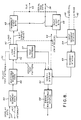
- Figure 3 is a schematic block diagram of a system for driving and verifying, in accordance with the invention, segmented digital displays of a capacitive nature.
- Figure 4 is a schematic logic diagram of the buffer driver of figure 3.
- Figure 5a is a schematic diagram of the current probe of figure 3 utilized in determining segment status.
- Figure 5b is a schematic diagram of an alternative current probe for use in the system of figure 3.
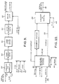
- Figure 6 is a detailed logic diagram of the Sample Control and Output Shift Register circuits of the system of figure 3.
- Figure 6a is an illustration of the current pulses measured with respect to on and off segments and the sample point utilized in the pulse mode of measurement.
- Figure 6b is an illustration of the sample point utilized in the square wave mode of operation for detecting shorted segments.
- Figure 7 is a top level data and control flow diagram for the system of figure 3.
- Figure 8 is a lower level data and control flow diagram of the Control Unit of figure 7 illustrating the primitive software elements thereof.
- Figure 9 is a lower level data and control flow diagram of the Drive LCD Unit of figure 7 which is implemented in hardware as illustrated in figure 3.
- Figure 10 ⁇ is a lower level data and control flow diagram of the Determine Segment Status Unit of figure 7 which is implemented in hardware as illustrated in figure 3.
- FIG. 1a seven segments a-g are illustrated arranged in a conventional array for providing one digit of a decimal digital numerical indicator. Selective energization of the segments a-g form the decimal digits 0 ⁇ -9.
- a malfunctioning segment or its associated circuitry which results in a segment being on when it should be off or off when it should be on, may result in a symbol that is clearly non-numeric thus representing to the user that a malfunction has occured. Conversely, however, such a malfunction may result in the display of a digit other than that commanded.
- a digital altitude indicator for aircraft an erroneous display of altitude to the pilot can precipitate an dangerous situation. For example, if the numeral 9 is commanded for which segments a-d, f and g should be on but segment f is erroneously off the numeral 3 is instead displayed.
- LCD material is sandwiched between two glass substrates 10 ⁇ and 11 on which transparent electrodes are deposited.
- a reflective surface 12 is deposited followed by a transparent electrode backplane 13.
- a polarizer 14 is deposited on the inner surface of the front substrate 10 ⁇ .
- transparent electrodes 15 forms a small capacitive element for each segment with respect to the backplane 13.
- electroluminescent displays have the same characteristics as the LCD since EL displays have a 5 layer sandwich construction comprising electrode, dielectric, phosphor, dielectric, and electrode.
- Both of these types of displays are driven by an alternating voltage which is typically a square wave with the "on" segment driven out of phase and the "off” segment driven in phase with the backplane. Since each segment is capacitive, the status of a segment can be measured, in accordance with the invention, by the existance or absence of a current pulse. Additionally an open connection between the driver and the segment is detectable as an off segment and a failure of the driver to a high or low state, that can source or sink current, is detectable as an on segment. The only coverage not provided is the mechanical leakage of the liquid crystal material from between the glass plates 10 ⁇ and 11 in the LCD and the fading of the phosphor luminescence in the EL display. Neither leakage in the LCD or phosphor fading in the EL display, however, is critical since data is not misrepresented.
- the LCD material sandwiched between the glass substrates 10 ⁇ and 11 includes liquid crystal molecules 16.
- Light entering the front glass substrate 10 ⁇ is polarized by the polarizer 14, reflected from the reflective surface 12 and retransmitted through the polarizer 14 to provide a silver appearance to the viewer.
- the liquid crystal molecules 16, in the vicinity of the energized electrode 15 experience a rotation or twist that rotates the axis of polarization as the polarized light is transmitted through the LCD material.
- This light is reflected from the reflective surface 12 but is blocked from reemerging through the front glass substrate 10 ⁇ by the polarizer 14 since the direction of polarization of this light is no longer coincident with the axis of polarization of the polarizer 14.
- the energized segment 15 provides a black appearance to the viewer, thereby displaying the LCD information.
- a 10 ⁇ 0 ⁇ Hz square wave source 20 ⁇ applies a 10 ⁇ 0 ⁇ Hz square wave to the backplane electrode 13 of the LCD.
- the 10 ⁇ 0 ⁇ Hz square wave is also applied directly and through an inverter 21 to an LCD segment electrode 15 via a single pole double throw switch 22.
- a current probe 23 is interposed between the switch 22 and the segment electrode 15.
- the segment command that determines if the segment should be on or off is applied to position the switch 22. When the switch 22 is in the off position the electrode 15 is driven by the 10 ⁇ 0 ⁇ Hz square wave in phase with the backplane electrode 13.
- the electrode 15 When the switch 22 is in the on position the electrode 15 is driven by the 10 ⁇ 0 ⁇ Hz square wave through the inverter 21 and is thus driven 180 ⁇ 0 ⁇ out of phase with the backplane electrode 13. Since an on segment electrode 15 is driven out of phase with the backplane electrode 13, the capacitive segment electrode 15 will be continually charging and discharging thus demanding current pulses. These current pulses are detected by the current probe 23 thus measuring the on status of the segment. Since an off segment electrode 15 is driven in phase with the backplane electrode 13, no current pulses are demanded. The current probe 23 detects this condition and provides a signal indicative of the off status of the segment. Thus, the current probe 23 verifies the status of the segments by the measurement of the current pulses required to charge the effective capacitance of each segment.
- Curve 26 depicts the current pulses detected for an off segment and curve 27 depicts the current pulses detected for an on segment. It is appreciated that the current pulses or spikes for an on segment are significantly larger in amplitude and greater in duration than those for an off segment.
- a control unit formats incoming display data into appropriate form for the segmented display.
- the control unit converts the data into serial format and provides it to the display by a serial bus structure.
- the serial interconnect interface between the control unit and the display simplifies the apparatus and permits the display to be located remotely from the control unit.
- the display unit inputs the serial display data, converts the data to parallel, buffers the data, and drives the backplane and each display segment.
- the 10 ⁇ 0 ⁇ Hz square wave oscillator 20 ⁇ ( Figure 2b) is utilized to drive the segments in phase with the backplane for an off segment and out of phase with the backplane for an on segment.
- Segment status determining circuitry utilizes the 10 ⁇ 0 ⁇ Hz signal as a clock to synchronize the measurement of the current pulses between the display drivers and the capacitive segments of the display.
- An on segment continually charges and discharges thus demanding current pulses.
- An off segment does not require current pulses. These current pulses are sensed as one's or zero's which are loaded into a shift register utilized to transmit the segment status data to the control unit via the serial bus structure.
- the serial status output data from the display is converted in the control unit to parallel and compared with the desired result.
- Two modes of operation are utilized. In one mode the output status data from the display is compared to the desired result each update frame of the control unit. Thus the control unit verifies segment status each time a frame of display data is transmitted to the display unit. In the second mode of operation, the control unit generates a test pattern which is transmitted to the display and the segment status data generated thereby is utilized to verify the display operational integrity.
- the display pattern alters and restores the display over a sufficiently short time interval that the human eye integration causes the pattern to be unnoticed by the user.
- the following chart provides a failure analysis depicting detection responses for all types of display failures.
- FIG. 3 a schematic block diagram of a system for driving and verifying an LCD in accordance with the invention is illustrated.
- the system of Figure 3 includes a Control Unit 30 ⁇ , a Drive LCD Unit 31, a Determine Segment Status Unit 32 and a 10 ⁇ 0 ⁇ Hz square wave clock 33.
- the Drive LCD Unit 31 provides segment driving signals to a liquid crystal display 34 via strip connectors 35.
- the LCD 34 comprises a plurality of display indicators with the backplane electrodes thereof receiving drive energization directly from the square wave clock 33.
- the Control Unit 30 ⁇ is preferably implemented by an 80 ⁇ 51 microprocessor 36 that receives display data from an external source, not shown, at a port 37. The display data is received in parallel and reformated by the control unit 30 ⁇ into Serial Segment Data transmitted to the Drive LCD Unit 31 by a serial bus 38.
- the 80 ⁇ 51 microprocessor 36 includes a main program 39 that provides overall control of the system.
- the main program 39 provides an interrupt signal on a line 40 ⁇ and a Select Test Pattern Control signal on a line 41.
- the microprocessor 36 reads a frame of update display data at the port 37.
- the microprocessor 36 loads the Serial Segment Data via the bus 38 into the Drive LCD Unit 31 and verifies the display utilizing the Determine Segment Status Unit 32.
- the main program 39 issues the Select Test Pattern Signal on the line 41 when the LCD 34 is to be verified with the test pattern.
- the microprocessor 36 issues a load signal on a line 42 to the Drive LCD Unit 31 as well as a clock signal (CLK) on a line 43, a chip select signal (CS0 ⁇ ) on a line 44 and a read signal on a line 45 to the Drive LCD Unit 31 and to the Determine Segment Status Unit 32.
- the microprocessor 36 also issues a SQ*/PUL signal on a line 46 to the Determine Segment Status Unit 32.
- the CS0 ⁇ signal on the line 44 is applied to AND gates 47,48, and 49 to enable the chip.
- the microprocessor 36 also issues chip enable signals CS1-CS4 to enable other display chips (not shown) in the system.
- the read signal on the line 45 is utilized by the microprocessor 36 to read the status of the segments from the Determine Segment Status Unit 32. Segment data is loaded when the microprocessor 36 is not reading status data. Thus, read-not is applied as an input to the AND gate 48 to enable the Drive LCD Unit 31 to receive the Serial Segment Data on the bus 38.
- the Drive Unit 31 includes a serial-in parallel-out input shift register 50 ⁇ coupled to the serial bus 38 to receive the Serial Segment Data at the serial input (SI) thereof.
- the input shift register 50 ⁇ receives the output of the AND gate 48 at the enable input thereof and the clock signal on the line 43 at the clock input thereof. Thus, when the read signal on the line 45 is low, the input shift register 50 ⁇ is enabled to receive the Serial Segment Data on the bus 38 which is clocked in by the clock signal on the line 43.
- the parallel output Q 0 ⁇ -Q N of the input shift register 50 ⁇ is applied in parallel to a parallel-in parallel-out display register 51.
- the display register 51 is clocked by the load signal on the line 42 applied through the AND gate 47.
- the parallel output DR 0 ⁇ -DR N of the display register 51 is applied to segment buffer drivers 52.
- the buffer drivers 52 are responsive to the square wave signal from the clock 33 and the respective data bits from the display register 51 to provide a square wave signal that is either in phase or out of phase with the clock 33 at each of the buffer driver outputs D 0 ⁇ -D N in a manner to be described.
- the buffer driver outputs are applied through respective current probes 53 and the strip connector 35 to the respective segments of the LCD 34.
- the current probes 53 are interposed between the buffer drivers 52 and the segments of the LCD 34, respectively, to provide the LCD segment drive via the outputs S 0 ⁇ -S N of the respective current probes 53 and the segment status signals via the current probe outputs I 0 ⁇ -I N .
- the segment status signals from the current probes 53 are applied as inputs to a parallel-in serial-out output shift register 54.
- the current probe outputs I 0 ⁇ -I N are strobed in parallel into the shift register 54 by a Sample Strobe signal on a line 55 from a Sample Control Circuit 56.
- the Sample Control Circuit 56 receives the SQ*/PUL signal on the line 46 to time the Sample Strobe on the line 55 in accordance with whether square wave or pulse mode segment status information is required by the microprocessor 36.
- the Sample Control Circuit 56 is also responsive to the square wave drive from the clock 33 for timing the Sample Strobe on the line 55.
- the serial output (SO) of the output shift register 54 is applied to the serial bus 38 so as to provide Serial Segment Status Data to the microprocessor 36.
- the microprocessor 36 issues CLK on the line 43 to the clock input of the output shift register 54 to clock the Serial Segment Status Data onto the bus 38.
- the read signal on the line 45 is applied via the AND gate 49 to enable the output shift register 54 and the Sample Control Circuit 56 when the microprocessor 36 requires Segment Status Data.
- the microprocessor 36 reformats the Serial Segment Status Data into a parallel structure for comparison with the input display data provided at the port 37 so as to provide error status signals with respect to the segments of the LCD 34, respectively.
- the microprocessor 36 contains software for inputting and issuing the data and control signals herein described.
- the primitive software elements are schematically illustrated as Input Segment Data 60 ⁇ , Load Display 61, Verify Display 62, Transmit 8 Bits 63, Input Segment Status 64, and Input 8 Bits 65.
- the microprocessor 36 also includes storage for Buffered Segment Data 66, Test Pattern 67, Error Maintenance Status 68, and Segment Status 69 as schematically illustrated. It is appreciated that the processes 60 ⁇ -65 with the exeception of Transmit 8 Bits 63 and Input 8 Bits 65 are performed by the system software in a manner to be described in further detail hereafter. Processes 63 and 65 are performed by the serial port hardware of the 80 ⁇ 51 microprocessor 36.
- the outputs DR 0 ⁇ -DR N from the display register 51 are applied as inputs to respective EXCLUSIVE OR gates 80 ⁇ .
- the other input to each of the gates 80 ⁇ is provided by the 10 ⁇ 0 ⁇ Hz square wave from the clock 33.
- the outputs of the EXCLUSIVE OR gates 80 ⁇ are applied as inputs to respective high voltage buffer drivers 81.
- the respective outputs of the buffer drivers 81, D 0 ⁇ -D N are applied to the current probes 53 respectively.
- the drivers 81 provide the high voltage buffers required for dichroic type LCD's.
- the buffer drivers 52 provide the process for driving the "on" segments out of phase with the backplane and the "off" segments in phase with the backplane.
- Figures 5a, 5b, 6, 6a, and 6b Details of the Determine Segment Status Unit 32 (Fig. 3) are illustrated in Figures 5a, 5b, 6, 6a, and 6b. Three basic elements are utilized; viz, the current probes of Figures 5a or 5b, the output shift register 54 and the Sample Control Circuit of Figure 6.
- Figures 6a and 6b illustrate waveforms and sample points illustrating the operations occuring in the SQ (square wave) mode and in the PUL (pulse) mode.
- Each current probe comprises a resistor 82 in series between the output of the buffer driver 52 and the LCD segment.
- a level detector 83 connected across the resistor 82 is set at 1/3 the peak current pulse.
- Figure 5b illustrates an alternative current probe for utilization in the preferred embodiment of the invention.
- Each current probe is comprised of a photo emitter 84 connected in series between the output of the buffer driver and the segment of the LCD.
- a photo detector 85 responsive to the light output of the photo emitter 84 is set at a threshold of 1/3 the peak current pulse.
- the outputs I O -I N of the current probes 53 are applied to the parallel input of the output shift register 54 wherein they are sampled at a time determined by the Sample Control 56.
- the Serial Segment Status Data provided at the serial output (SO) of the output shift register 54 is clocked onto the serial bus 38 by the clock signal from the microprocessor 36 on the line 43.
- the read signal on the line 45 and the chip select signal, CS0 ⁇ , on the line 44 enable the output shift register 54 via the AND gate 49.
- the output of the AND gate 49 is also applied as an input to an AND gate 86 to enable the Sample Control 56.
- the output of the AND gate 86 triggers a Sample Strobe circuit 87 to provide the Sample Strobe to the output shift register 54 on the line 55.
- the 10 ⁇ 0 ⁇ Hz square wave from the clock 33 through a 2.5 microsecond delay element 88 and through a 30 ⁇ microsecond delay element 89 is applied as inputs to AND gates 90 ⁇ and 91 respectively.
- the SQ*/PUL signal on the line 46 is applied as an input to the AND gate 90 ⁇ and through and inverting input to the AND gate 91.
- the SQ*/PUL signal enables the AND gate 90 ⁇ and disables the AND gate 91.
- the SQ*/PUL signal enables the AND gate 91 and disables the AND gate 90 ⁇ .
- the outputs of the AND gates 90 ⁇ and 91 provide inputs to an OR gate 92 which in turn provides an input to the AND gate 86.
- the SQ*/PUL control signal on the line 46 provided by the Control Unit 30 ⁇ to the Sample Control Circuit 56 selects the type of sample to be verified.
- the Sample Control Circuit 56 provides the necessary delay of the 10 ⁇ 0 ⁇ Hz display clock to strobe the sample line 55 to the output shift register 54.
- FIG. 7 a top level data and control flow diagram of the system of Figure 3 for driving an LCD and verifying its status is illustrated.
- the control signals illustrated in dashed line are required to achieve the data flow illustrated in solid line.
- the Control Unit 30 ⁇ receives Display Data from an external source. The data is reformated by the Control Unit 30 ⁇ into Serial Segment Data and transmitted to the Drive LCD Unit 31 via the serial bus 38.
- the Control Unit 30 ⁇ also loads the store Error Maintenance Status 68 ( Figure 3) with the LCD error status.
- the Drive LCD Unit 31 supplies the Backplane energization and LCD Data to be transmitted to the LCD 34 (Fig. 3) utilizing the 10 ⁇ 0 ⁇ Hz clock 33.
- Determine Segment Status Unit 32 inserts a current probe in series with the LCD Data to LCD Output path, sampling for current pulses timed by the 10 ⁇ 0 ⁇ Hz clock 33.
- the Determine Segment Status Unit 32 then transmits to the Control Unit 30 ⁇ the Serial Segment Data, via the serial bus 38, containing the segment status information.
- the clock signal (CLK) on the line 43 is a timing control utilized to synchronize data bits between the Control Unit 30 ⁇ , the Drive LCD Unit 31, and the Determine Segment Status Unit 32.
- CS0 ⁇ , on the line 44 is a chip select control signal utilized to activate one of a multiplicity of displays and drives. Only one display activated by CS0 ⁇ is illustrated herein for simplicity.
- the Select Test Pattern signal on the line 41 is a control signal provided by the main program utilized to select the Control Unit 30 ⁇ mode of operation. As discussed above, the two selectable modes are; 1) sample and verify the display status after each update frame and, 2) at regular intervals issue and verify a test pattern for the Serial Segment Data.
- the SQ*/PUL signal on the line 46 is utilized to select segment status detection delays for square wave or pulse current detection.
- FIG. 8 a lower level diagram is illustrated depicting the data flows, processes and control flows associated with the operation of the Control Unit 30 ⁇ .
- the data flow signals are illustrated in solid line and the control flow signals are illustrated in dashed line.
- the processes 60 ⁇ , 61, 62, and 64 are performed by software and the processes 63 and 65 are performed by the serial port hardware of the 80 ⁇ 51 microprocessor 36 ( Figure 3).
- the operational description of each process, in Structured English, is as follows:
- the input shift register 50 ⁇ (Fig. 3) is represented by the combination of Convert to Parallel 56 and the Store-Temp Serial Data 50 ⁇ .
- Serial Segment Data on the serial bus 38 is clocked in on the rising edge of CLK on the line 43.
- the Load LCD Drive 51 combined with the Store-LCD Segment Data 51 from a latch which is implemented by the display register 51 of Figure 3. This latch is clocked on the rising edge of the load signal on the line 42.
- the Drive LCD 52 implemented by the buffer driver 52 of Figure 3, continually accesses the latched output from LCD Segment Data and provides the drive to the LCD segments.
- FIG. 10 ⁇ lower level data and control flow details of the Determine Segment Status Unit 32 are illustrated.
- the current probes 53 ( Figure 3) on the LCD Data Segment Drives and the Sample Control Circuit 56 that measures the current pulses are represented by Measure Segment Status 53, 56.
- the output shift register 54 ( Figure 3) is represented by Convert to Serial 54.
- CS0 ⁇ on the line 44 and read on the line 45 are enables provided by the Control Unit 30 ⁇ when Segment Status Data is required.
- SQ*/PUL on the line 46 modifies the time delay in sampling the current as controlled by Measure Segment Status 53, 56.
- Measure Segment Status 53, 56 issues a Sample Strobe on the line 55 to Convert to Serial 54 when a sample is to be taken.
- the present invention provides a system for displaying and verifying information with respect to segmented displays having a capacitive nature such as Liquid Crystal Displays or Electroluminescent Displays. Verification is automatic with each display update and is performed without user intervention or distraction.
- the invention provides an automatic fault self detection system.
Landscapes
- Engineering & Computer Science (AREA)
- Theoretical Computer Science (AREA)
- Physics & Mathematics (AREA)
- Computer Hardware Design (AREA)
- General Physics & Mathematics (AREA)
- General Engineering & Computer Science (AREA)
- Quality & Reliability (AREA)
- Control Of Indicators Other Than Cathode Ray Tubes (AREA)
- Liquid Crystal Display Device Control (AREA)
- Control Of El Displays (AREA)
- Liquid Crystal (AREA)
- Testing Of Short-Circuits, Discontinuities, Leakage, Or Incorrect Line Connections (AREA)
Claims (9)
- Vorrichtung zur Überprüfung des Betriebszustandes einer digitalen Anzeige (34), die auf Eingangs-Anzeigedaten anspricht, wobei die Anzeige Anzeigesegmente mit einem kapazitiven Charakter aufweist, und die Anzeigesegmenttreiber (52) zum Anlegen von Anregungssignalen an die Segmente in Übereinstimmung mit den Eingangs-Anzeigedaten aufweist, gekennzeichnet durch :
eine Steuereinheit (30) mit Mitteln (36,67) für die Erzeugung der Anregungssignale als ein Testmuster zum Überprüfen des Betriebszustandes der digitalen Anzeige;
eine Segmentstatus-Feststelleinrichtung (32) mit Stromtasteinrichtungen (53), die die Treiber (52) an die Segmente ankoppeln, um Stromimpulse festzustellen, die aus der Anlegung der Anregungssignale durch die Steuereinheit an die Segmente resultieren, wobei die Segmentstatus-Feststelleinrichtung Mittel (55,56) aufweist, um Segmentstatussignale in Übereinstimmung mit den Stromimpulsen vorzugeben;
und wobei die Steuereinheit (30) eine Vergleichseinrichtung aufweist, um die Segmentstatussignale mit den Anregungssignalen zu vergleichen und Diskrepanzen dazwischen festzustellen. - Vorrichtung nach Anspruch 1, dadurch gekennzeichnet, daß die Stromimpulse für ein eingeschaltetes Segment eine wesentlich größere Amplitude als die Stromimpulse für ein ausgeschaltetes Segment aufweisen.
- Vorrichtung nach Anspruch 2, dadurch gekennzeichnet, daß die Stromtasteinrichtung (53) umfaßt:
einen Widerstand (82), der den Treiber (52) mit dem Segment verbindet, und
einen Pegeldetektor (83), der an den Widerstand (82) angeschlossen ist und einen Schwellwert besitzt, um zwischen den Stromimpulsen für die eigeschalteten Segmente und den Stromimpulsen für die ausgeschalteten Segmente zu unterscheiden. - Vorrichtung nach Anspruch 2, dadurch gekennzeichnet, daß die Stromtasteinrichtung (53) umfaßt:
einen Photoemitter (84), der den Treiber (52) an das Segment anschließt, und
einen Photodetektor (85), der optisch mit dem Photoemitter (84) gekoppelt ist und einen Schwellwert besitzt, der so eingestellt ist, um zwischen Stromimpulsen für die eingeschalteten Segmente und den Stromimpulsen für die ausgeschalteten Segmente zu unterscheiden. - Vorrichtung nach Anspruch 1, dadurch gekennzeichnet, daß die Mittel zur Vorgabe der Segmentstatussignale eine Abtaststeuereinrichtung (56) für die Vorgabe eines Abtastsignales umfassen, um die Abtastung der Stromtasteinrichtung zu steuern.
- Vorrichtung nach Anspruch 5, dadurch gekennzeichnet, daß die Abtasteinrichtung (56) Mittel (86-92) umfaßt, um selektiv das Abtastsignal zur Abtastung der Stromtasteinrichtung (53,54) während der Dauer der Stromimpulse für das eingeschaltete Segment vorzugeben und um die Stromtasteinrichtung zu einem Zeitpunkt abzutasten, zu dem ein Stromimpuls für ein eingeschaltetes Segment beendet sein sollte.
- Vorrichtung nach Anspruch 1, dadurch gekennzeichnet, daß die Steuereinheit (30) die Eingangs-Anzeigedaten in parallelem Format empfängt und daß die Steuereinheit Mittel (36) für die Umwandlung dieser parallelen Eingangs-Anzeigedaten in serielles Format umfaßt.
- Vorrichtung nach Anspruch 7, dadurch gekennzeichnet, daß die Anzeige einen Serien/Parallel-Wandler (50,51) für die Vorgabe von Steuersignalen an die entsprechenden Segmenttreiber (52) umfaßt und daß die Vorrichtung einen seriellen Bus (38) aufweist, der die Steuereinheit (30) mit der Anzeige verbindet, um die Eingangs-Anzeigedaten in seriellem Format an den Serien/Parallel-Wandler zu übertragen.
- Vorrichtung nach Anspruch 8, dadurch gekennzeichnet, daß die Mittel zur Vorgabe der Segmentstatussignale einen Parallel/Serien-Wandler (54) umfassen, der auf die Stromtasteinrichtung (53) anspricht, um die Segmentstatussignale in serielles Format für die Übertragung zu der Steuereinheit (30) über den seriellen Bus (38) umzuwandeln.
Applications Claiming Priority (2)
| Application Number | Priority Date | Filing Date | Title |
|---|---|---|---|
| US169540 | 1988-03-17 | ||
| US07/169,540 US4951037A (en) | 1988-03-17 | 1988-03-17 | Display segment fault detection apparatus |
Publications (3)
| Publication Number | Publication Date |
|---|---|
| EP0333136A2 EP0333136A2 (de) | 1989-09-20 |
| EP0333136A3 EP0333136A3 (de) | 1991-03-20 |
| EP0333136B1 true EP0333136B1 (de) | 1994-08-31 |
Family
ID=22616129
Family Applications (1)
| Application Number | Title | Priority Date | Filing Date |
|---|---|---|---|
| EP89104519A Expired - Lifetime EP0333136B1 (de) | 1988-03-17 | 1989-03-14 | Gerät zur Erkennung von Fehlern eines Anzeigesegments |
Country Status (5)
| Country | Link |
|---|---|
| US (1) | US4951037A (de) |
| EP (1) | EP0333136B1 (de) |
| JP (1) | JP2756817B2 (de) |
| CA (1) | CA1331058C (de) |
| DE (1) | DE68917758T2 (de) |
Cited By (2)
| Publication number | Priority date | Publication date | Assignee | Title |
|---|---|---|---|---|
| US7561144B2 (en) | 2003-11-25 | 2009-07-14 | Sorin Group Deutschland Gmbh | Touch-sensitive input device and fault detection device for a touch-sensitive input device, in particular for medico-technical devices |
| US11462140B2 (en) | 2020-09-30 | 2022-10-04 | GE Precision Healthcare LLC | Methods and systems for detecting a malfunctioning display device |
Families Citing this family (17)
| Publication number | Priority date | Publication date | Assignee | Title |
|---|---|---|---|---|
| US5319786A (en) * | 1987-05-20 | 1994-06-07 | Hudson Soft Co., Ltd. | Apparatus for controlling a scanning type video display to be divided into plural display regions |
| FR2680595B1 (fr) * | 1991-08-21 | 1993-11-26 | Satam | Dispositif de controle de segment pour afficheur a cristaux liquides, et procede de controle correspondant. |
| US5184082A (en) * | 1991-09-18 | 1993-02-02 | Honeywell Inc. | Apparatus and method for testing an active matrix pixel display |
| JP3118682B2 (ja) * | 1992-12-25 | 2000-12-18 | キヤノン株式会社 | 液晶表示装置 |
| GB9308294D0 (en) * | 1993-04-22 | 1993-06-09 | Gilbarco Ltd | Error detection apparatus for an electro-optic display |
| EP0713100A1 (de) * | 1994-11-15 | 1996-05-22 | AT&T GLOBAL INFORMATION SOLUTIONS INTERNATIONAL INC. | Fehlererkennender elektronischer Anzeigemodul |
| US5767454A (en) * | 1996-10-22 | 1998-06-16 | Ncr Corporation | Electronic scale including a fault-detecting electronic display module |
| US5812102A (en) * | 1997-03-12 | 1998-09-22 | Union Switch & Signal Inc. | Vital monitoring system for seven-segment display used in railroad applications |
| JP2004500731A (ja) | 1998-06-18 | 2004-01-08 | ソニー エレクトロニクス インク | 複数のディスプレイ装置に亘ってビデオ及び/又はグラフィック画像を分割し、スケーリングし、表示する方法及び装置 |
| US6097302A (en) * | 1999-06-23 | 2000-08-01 | Union Switch & Signal, Inc. | System and method for monitoring a plural segment light-emitting display |
| US7348690B2 (en) * | 2002-02-25 | 2008-03-25 | Alfred Wade Muldoon | Preventing unsafe operation by monitoring switching means |
| JPWO2015132908A1 (ja) * | 2014-03-05 | 2017-03-30 | パイオニア株式会社 | 表示制御装置 |
| US10832604B2 (en) | 2016-04-22 | 2020-11-10 | Nec Display Solutions, Ltd. | Video monitoring method, display device, and display system |
| JP7371455B2 (ja) * | 2019-11-21 | 2023-10-31 | セイコーエプソン株式会社 | 駆動回路、表示モジュール、及び移動体 |
| CN110940906B (zh) * | 2019-12-26 | 2025-03-11 | 烟台持久钟表有限公司 | 一种数码管运行状态检测系统及自诊断方法 |
| JP7593050B2 (ja) * | 2020-10-26 | 2024-12-03 | セイコーエプソン株式会社 | 表示装置、電子機器及び移動体 |
| EP4278869A1 (de) * | 2021-01-13 | 2023-11-22 | Lichtwart GmbH | Verfahren und steuervorrichtung zur steuerung einer lichtanlage |
Family Cites Families (6)
| Publication number | Priority date | Publication date | Assignee | Title |
|---|---|---|---|---|
| JPS5189348A (de) * | 1975-02-04 | 1976-08-05 | ||
| NL171845C (nl) * | 1977-02-18 | 1983-05-16 | Philips Nv | Gasontladingsweergeefinrichting. |
| CH627575A5 (de) * | 1978-06-09 | 1982-01-15 | Mettler Instrumente Ag | Multisegment-fluessigkristall-anzeige mit einer funktionsueberwachungsschaltung. |
| DE2951584A1 (de) * | 1979-12-21 | 1981-07-16 | Kienzle Apparate Gmbh, 7730 Villingen-Schwenningen | Verfahren und anordnung zur ansteuerung, ueberwachung und kontrolle des betriebes einer weitgehend passiven datenanzeige, insbesondere z.b. einer fluessigkristallanzeige (lcd-anzeige) |
| DE3026848A1 (de) * | 1980-07-16 | 1982-02-04 | Kienzle Apparate Gmbh, 7730 Villingen-Schwenningen | Ueberwachungsschaltung zur kontrolle der anschluesse von lcd-anzeigen |
| DE3043723A1 (de) * | 1980-11-20 | 1982-06-24 | Pfister Gmbh, 8900 Augsburg | Verfahren und vorrichtung zur ueberpruefung der funktionen eines anzeigesystems |
-
1988
- 1988-03-17 US US07/169,540 patent/US4951037A/en not_active Expired - Lifetime
-
1989
- 1989-02-27 CA CA000592910A patent/CA1331058C/en not_active Expired - Fee Related
- 1989-03-14 EP EP89104519A patent/EP0333136B1/de not_active Expired - Lifetime
- 1989-03-14 DE DE68917758T patent/DE68917758T2/de not_active Expired - Fee Related
- 1989-03-17 JP JP1065799A patent/JP2756817B2/ja not_active Expired - Fee Related
Cited By (2)
| Publication number | Priority date | Publication date | Assignee | Title |
|---|---|---|---|---|
| US7561144B2 (en) | 2003-11-25 | 2009-07-14 | Sorin Group Deutschland Gmbh | Touch-sensitive input device and fault detection device for a touch-sensitive input device, in particular for medico-technical devices |
| US11462140B2 (en) | 2020-09-30 | 2022-10-04 | GE Precision Healthcare LLC | Methods and systems for detecting a malfunctioning display device |
Also Published As
| Publication number | Publication date |
|---|---|
| US4951037A (en) | 1990-08-21 |
| JP2756817B2 (ja) | 1998-05-25 |
| DE68917758D1 (de) | 1994-10-06 |
| CA1331058C (en) | 1994-07-26 |
| DE68917758T2 (de) | 1995-02-09 |
| EP0333136A3 (de) | 1991-03-20 |
| EP0333136A2 (de) | 1989-09-20 |
| JPH0234893A (ja) | 1990-02-05 |
Similar Documents
| Publication | Publication Date | Title |
|---|---|---|
| US4951037A (en) | Display segment fault detection apparatus | |
| US4311993A (en) | Multisegment liquid crystal indication system | |
| US5515390A (en) | Error detection apparatus for an electro-optic display | |
| US4541066A (en) | Method and apparatus for checking the functions of a display system | |
| US4247852A (en) | Monitoring system for indicators utilizing individually energizable segments | |
| US5268635A (en) | Intelligent self-diagnosing and sparing light emitting diodes | |
| US4734688A (en) | Methods and means for testing faults in a liquid crystal display system | |
| GB2075737A (en) | A liquid crystal display device | |
| KR100414522B1 (ko) | 점검기능을 갖는 전광판 및 에러검출방법 | |
| CN114373412A (zh) | 一种显示装置及其异常检测方法 | |
| US4188626A (en) | Method for scanning a keyboard and for actuating a display device via common conductors | |
| US5113130A (en) | Testing operation of electric energy meter optics system | |
| US5268633A (en) | Testing operation of electric energy meter optics system | |
| US4255804A (en) | Electronic watch | |
| KR102174972B1 (ko) | 고장 검출 가능한 발광 소자 어레이 | |
| EP0135331A2 (de) | System und Technik zur Prüfung von Flüssigkristallanzeigen | |
| US4829521A (en) | Test circuit for detecting short duration pulses | |
| GB2080593A (en) | Monitoring circuit for checking the connections of liquid crystal displays | |
| US6295621B1 (en) | Apparatus for detecting output bond integrity in a display driver circuit | |
| US4618965A (en) | Monitoring of data transfer system having serially distributed data ports | |
| JPH0415474B2 (de) | ||
| US6188672B1 (en) | Circuit arrangement for sensing errors in bit patterns | |
| JPS6323194A (ja) | 液晶デイスプレイ装置用検査方法および装置 | |
| CN111402770A (zh) | 显示装置的测试装置 | |
| JP2512325B2 (ja) | ファン故障検出装置 |
Legal Events
| Date | Code | Title | Description |
|---|---|---|---|
| PUAI | Public reference made under article 153(3) epc to a published international application that has entered the european phase |
Free format text: ORIGINAL CODE: 0009012 |
|
| AK | Designated contracting states |
Kind code of ref document: A2 Designated state(s): DE FR GB IT NL |
|
| PUAL | Search report despatched |
Free format text: ORIGINAL CODE: 0009013 |
|
| AK | Designated contracting states |
Kind code of ref document: A3 Designated state(s): DE FR GB IT NL |
|
| 17P | Request for examination filed |
Effective date: 19910812 |
|
| 17Q | First examination report despatched |
Effective date: 19931026 |
|
| GRAA | (expected) grant |
Free format text: ORIGINAL CODE: 0009210 |
|
| AK | Designated contracting states |
Kind code of ref document: B1 Designated state(s): DE FR GB IT NL |
|
| PG25 | Lapsed in a contracting state [announced via postgrant information from national office to epo] |
Ref country code: FR Free format text: THE PATENT HAS BEEN ANNULLED BY A DECISION OF A NATIONAL AUTHORITY Effective date: 19940831 |
|
| REF | Corresponds to: |
Ref document number: 68917758 Country of ref document: DE Date of ref document: 19941006 |
|
| ET | Fr: translation filed | ||
| ITF | It: translation for a ep patent filed | ||
| PG25 | Lapsed in a contracting state [announced via postgrant information from national office to epo] |
Ref country code: GB Effective date: 19950314 |
|
| PLBE | No opposition filed within time limit |
Free format text: ORIGINAL CODE: 0009261 |
|
| STAA | Information on the status of an ep patent application or granted ep patent |
Free format text: STATUS: NO OPPOSITION FILED WITHIN TIME LIMIT |
|
| 26N | No opposition filed | ||
| PG25 | Lapsed in a contracting state [announced via postgrant information from national office to epo] |
Ref country code: NL Effective date: 19951001 |
|
| GBPC | Gb: european patent ceased through non-payment of renewal fee |
Effective date: 19950314 |
|
| NLV4 | Nl: lapsed or anulled due to non-payment of the annual fee |
Effective date: 19951001 |
|
| PG25 | Lapsed in a contracting state [announced via postgrant information from national office to epo] |
Ref country code: DE Effective date: 19951201 |
|
| REG | Reference to a national code |
Ref country code: FR Ref legal event code: ST |
|
| PG25 | Lapsed in a contracting state [announced via postgrant information from national office to epo] |
Ref country code: IT Free format text: LAPSE BECAUSE OF NON-PAYMENT OF DUE FEES;WARNING: LAPSES OF ITALIAN PATENTS WITH EFFECTIVE DATE BEFORE 2007 MAY HAVE OCCURRED AT ANY TIME BEFORE 2007. THE CORRECT EFFECTIVE DATE MAY BE DIFFERENT FROM THE ONE RECORDED. Effective date: 20050314 |