EP0332448A2 - Superconductive optoelectronic devices - Google Patents
Superconductive optoelectronic devices Download PDFInfo
- Publication number
- EP0332448A2 EP0332448A2 EP89302357A EP89302357A EP0332448A2 EP 0332448 A2 EP0332448 A2 EP 0332448A2 EP 89302357 A EP89302357 A EP 89302357A EP 89302357 A EP89302357 A EP 89302357A EP 0332448 A2 EP0332448 A2 EP 0332448A2
- Authority
- EP
- European Patent Office
- Prior art keywords
- superconductive
- photoconductive
- region
- gate region
- photoconductivity
- Prior art date
- Legal status (The legal status is an assumption and is not a legal conclusion. Google has not performed a legal analysis and makes no representation as to the accuracy of the status listed.)
- Granted
Links
Images


Classifications
-
- H—ELECTRICITY
- H10—SEMICONDUCTOR DEVICES; ELECTRIC SOLID-STATE DEVICES NOT OTHERWISE PROVIDED FOR
- H10N—ELECTRIC SOLID-STATE DEVICES NOT OTHERWISE PROVIDED FOR
- H10N60/00—Superconducting devices
- H10N60/10—Junction-based devices
- H10N60/128—Junction-based devices having three or more electrodes, e.g. transistor-like structures
-
- H—ELECTRICITY
- H10—SEMICONDUCTOR DEVICES; ELECTRIC SOLID-STATE DEVICES NOT OTHERWISE PROVIDED FOR
- H10N—ELECTRIC SOLID-STATE DEVICES NOT OTHERWISE PROVIDED FOR
- H10N60/00—Superconducting devices
- H10N60/80—Constructional details
- H10N60/84—Switching means for devices switchable between superconducting and normal states
-
- Y—GENERAL TAGGING OF NEW TECHNOLOGICAL DEVELOPMENTS; GENERAL TAGGING OF CROSS-SECTIONAL TECHNOLOGIES SPANNING OVER SEVERAL SECTIONS OF THE IPC; TECHNICAL SUBJECTS COVERED BY FORMER USPC CROSS-REFERENCE ART COLLECTIONS [XRACs] AND DIGESTS
- Y10—TECHNICAL SUBJECTS COVERED BY FORMER USPC
- Y10S—TECHNICAL SUBJECTS COVERED BY FORMER USPC CROSS-REFERENCE ART COLLECTIONS [XRACs] AND DIGESTS
- Y10S505/00—Superconductor technology: apparatus, material, process
- Y10S505/70—High TC, above 30 k, superconducting device, article, or structured stock
- Y10S505/701—Coated or thin film device, i.e. active or passive
- Y10S505/702—Josephson junction present
-
- Y—GENERAL TAGGING OF NEW TECHNOLOGICAL DEVELOPMENTS; GENERAL TAGGING OF CROSS-SECTIONAL TECHNOLOGIES SPANNING OVER SEVERAL SECTIONS OF THE IPC; TECHNICAL SUBJECTS COVERED BY FORMER USPC CROSS-REFERENCE ART COLLECTIONS [XRACs] AND DIGESTS
- Y10—TECHNICAL SUBJECTS COVERED BY FORMER USPC
- Y10S—TECHNICAL SUBJECTS COVERED BY FORMER USPC CROSS-REFERENCE ART COLLECTIONS [XRACs] AND DIGESTS
- Y10S505/00—Superconductor technology: apparatus, material, process
- Y10S505/70—High TC, above 30 k, superconducting device, article, or structured stock
- Y10S505/701—Coated or thin film device, i.e. active or passive
- Y10S505/703—Microelectronic device with superconducting conduction line
Definitions
- This invention relates to a number of superconductive optoelectronic device and a superconductive optoelectronic apparatus.
- the superconductive optoelectronic devices and apparatuses of the invention are novel and vastly different from those of prior art in that the invention uses a combination of superconductive material and special superconductive photoconductive-material which reveals photoconductivity below the critical temperature of the relevant superconductive material.
- a number of new electronic devices and optoelectronic apparatuses may be developed, for instance, a switching device with no power loss, an optically operating device with no power loss, an optically operating logical device, a space parallel type optically operating apparatus, a camera or an image forming device possibly with superconducting wiring, a high-speed optically operating apparatus to be driven at an extremely low power, and the like.
- the superconductive photoconductive-oxide materials are so far electric insulators at room temperature, but when they are cooled down to the temperatures below the transition points of superconductive materials related to them, they reveal photoconductivity, i.e., they produce photo carriers and their conductivity varies depending on the intensity of the excitation light which is incident thereto.
- a power-loss-free useful superconductive optoelectronic device can be formed by combining a superconductive photoconductive-material of for instance the Ca-Sr-Bi-Cu-O system with its related superconductive material of for instance the Ca-Sr-Bi-Cu-O system.
- superconductive optoelectronic device is an optoelectronic device made of a combination of a superconductive material of one oxide system and that superconductive photoconductive-material of the same oxide system which reveals photoconductivity at temperatures below the critical temperatures of the superconductive material.
- An object of the invention is to provide a novel superconductive optoelectronic device by using effectively the optical properties of that superconductive photoconductive-material which is discovered by the inventor.
- the invention is neither a mere improvement of the prior art nor a simple solution of problems existing in the prior art, but an entirely new achievement.
- a superconductive optoelectronic device for instance, comprises a substrate, a photoconductive gate region formed on the substrate, and a source region and a drain region formed on the substrate at opposite sides of the gate region respectively so as to face toward each other across the gate region.
- the source and drain regions are made of a superconductive material
- the gate region is made of a superconductive photoconductive-material which reveals photoconductivity at temperatures below the critical temperature for superconductivity of the superconductive material
- the superconductive photoconductive-material and the superconductive material are of the same general chemical formula but with different contents of constituent elements.
- Bias source may be connected across the source region and the drain region of the optoelectronic devices of the invention, so as to drive an electric current through its photoconductive gate region depending on the intensity of light which is incident to the photoconductive gate region.
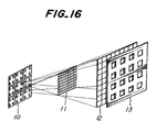
- 1 is a substrate, 2 a gate region, 3 a source region, 4 a drain region, 5 an insulating layer, 6 a conductive glass layer, 10 an alley-like light source, 11 a coding image-mask pattern, 12 a correlative image screen, and 13 is a decoding mask optical element alley.
- the inventor's experiments and analyses on the photoconductivity and superconductivity of various superconductive materials showed that a certain portions of superconductive materials in their phase diagram reveal photoconductivity complementary to or as well as superconductivity at temperature below their regions of transition temperatures from normal conductivity to superconductivity. For instance, in the case of superconductive oxides of the Ca-Sr-Bi-Cu-O system, the inventors discovered that with changing Sr content their superconductivity can be converted into photoconductivity at temperatures below their critical temperatures.
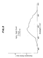
- Figure 1 illustrates typical results of experiments on the superconductivity and photoconductivity of the Ca-Sr-Bi-Cu-O system oxides.
- the curve (a) in Fig. 1 shows the temperature dependence of photoconductivity of Bi2O3 ceramics which is a reference substance clarified by the inventor.
- the Ca-Sr-Bi-Cu-O system reveals superconductivity if, e.g., its content x of Sr is in the range of 0.7 ⁇ 1 ⁇ x ⁇ 2, and if its content x of Sr is smaller than 0.7 ⁇ 1 such superconductivity disappears and it reveals complementary photoconductivity at temperature regions below their transition temperatures.
- an optoelectronic element of FET-like shape is formed by making a gate region with a superconductive photoconductive-material while making a source region and a drain region with a relevant superconductive material, an output current whose magnitude varies depending on the wavelength and intensity of light incident to the gate region can be produced so as to flow across the source and drain regions. If such an optoelectronic device is sustained at a temperature below the transition temperature of its superconductive material, it must work as a superconductive optoelectronic device which can be used in numerous ways; for instance, as a power-loss-free optical switching device with high-speed response, an optical detector, an optical signals amplifying device, or the like.
- Fig. 6 shows test results on its superconductivity and photoconductivity.
- z ⁇ 6.5 is a merely rough indication of the boundary not clearly and should not be taken exactly, since the superconductive defined photoconductive-area are continuously close to the superconductive-areas in thier phase diagram. Similar situations are the cases also for the other systems as far as the oxygen content z concerns.
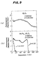
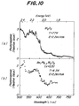
- Oxide material of Ba-Pb-Bi-O system will be described now by referring to Fig. 9 and Fig. 10.
- Curves (a) and (b) in Fig. 9 show the temperature dependences of photoresponse Q (T, ⁇ ) of a reference substance Bi2O3 ceramics and oxide specimens with a general chemical formula of Ba1-Pb 1-x -Bi x O z , respec tively.
- the inventor found that they reveal superconductivity under the conditions of 0.20 ⁇ x ⁇ 0.35 and 2.81 ⁇ z ⁇ 3, while they reveal photoconductivity under the conditions of x ⁇ 0.35 and 2.7 ⁇ z ⁇ 2.81.
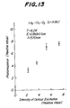
- Fig. 13 shows the relationship between the photoconductivity and the quantity of incident light (i.e., excitation light intensity) for the above oxide with z ⁇ 3.88. It can be seen from Fig. 13 that the photoresponse current clearly increases with the intensity of incident light.
- Fig. 14 is a schematic diagram showing the structure of an embodiment of the superconductive optoelectronic device according to the invention.
- the embodiment is a superconductive phototransistor in which a positive gate voltage V G is used (V G ⁇ 0).
- a substrate 1 is made of SrTiO3, and a photoconductive gate region 2 is formed on the substrate 1 with superconductive photoconductive-material Ca2-Bi1-Cu2-O z .
- the photoconductive gate region 2 has a width of 0.2 ⁇ m to 1.0 mm and a thickness of 1-10 ⁇ m.
- the above superconductive photoconductive-material Ca2-Bi1-Cu2-O z reveals photoconductivity in response to excitation by incident light of wavelength at least ⁇ 540-740 nm at a temperature below the transition temperature of a superconductive substance Ca1-Sr1-Bi1-Cu2-O z .
- a source region 3 and a drain region 4 are formed with Ca1-Sr1- Bi1-Cu2-O z oxide which reveals superconductivity below its critical temperature of 80K or 105-115 K.
- An electrically insulating layer 5 which is optically transparent is formed so as to cover top surfaces of the gate resion 2, the source region 3, and the drain region 4.
- the insulating layer 5 of the illustrated example was a 1 ⁇ m thick SiO2 film or mylar sheet. Further, a conductive surface of glass layer 6, for instance made of a NESA (Trademark of Pittsburgh Plate Glass Company) glass layer, is placed on the insulating layer 5, and electrodes are deposited on the conductive surface of glass layer 6.
- NESA Trademark of Pittsburgh Plate Glass Company
- a source for bias voltage V G is connected across the source region 3 and electrodes of the conductive surface of glass layer and a source for source-drain voltage V SD is connected between the source region 3 and the drain region 4 across the gate region 2.
- the superconducting optoelectronic element of Fig. 14 is cooled to a temperature below the critical temperatures, i.e., about 80K or 105-115K, of the superconducting zones of Ca 2-x -Sr x -Bi1-Cu2-O z and excitation light signals in a wavelength range is irradiated to the gate region 2.
- a pulsed dye ;aser of 3 nsec width can be used for an excitation light source. This fact basically indicates a high speed response of the device itself.
- photocarriers are generated in the gate region 2 depending on the photon number or intensity of light incident thereto.
- the generated carriers are accelerated by the source-drain voltage V SD so as to produce an induced output current which is delivered to an output resistor R. Accordingly, an output voltage due to incident photosignals appears across the resistor R.
- the amount and density of optically excited carriers in the gate region 2 can be variable depending not only on the photon number or intensity of incident light thereto but also the bias voltage V G , and the bias voltage V G can be harmoniously adjusted so as to meet specific requirements from users .
- photocarrier density of the order e.g., of 1012/cm3 can be obtainable in a surface layer of the gate region 2.
- the superconducting optoelectronic device of Fig. 14 can be used as a superconductive switching device.
- the source region 3 and the drain region 4 made of superconductive material are free from heat generation during operation, so that the optoelectronic device of Fig. 14 possesses those advantages which are inherent to superconductivity.
- Fig. 15 is a partial schematic diagram of an embodiment of the superconductive optoelectronic device of the invention, in which device a number of the superconductive optoelectronic devices of Fig. 16 are integrated at a high density in the form of one- or two-dimensional alleys. If wiring among different devices in the device of Fig. 15 is made by using superconducting material, heat generation in the alley or apparatus can be suppressed to an extremely low level.
- the superconducting optoelectronic device and apparatus of the invention can be used in various fields; for instance, as a loss free pick up (or camera) devices, loss-free detectors of optical signals in an optical computer which executes parallel operations in a spatially arranged manner, and the like.
- the device of the invention can be also used in a multiple channel system which selectively utilizes a number of different wavelengths in the incident light.
- Fig. 16 schematically illustrates an optical calculation procedure in a projection-correlative optical system of a space parallel optical computer in which system the superconductive optoelectronic devices of the invention are used.
- alley-like light source 10 projects a number of optical signals in parallel onto a coding mask pattern 11.
- the mask pattern 11 carries coding image signals in a mask fashion, which signals correspond to the type of operation to be superposed to the light beams.
- the light beams pass a correlative image screen 12 and then enter in parallel into the corresponding devices in a decoding mask optical device alley 13.
- Each optical device receives a coded signal which is modulated by the mask screen, and operated results can be obtained from the optoelectronic output signals from each of the optical devices.
- each optical device of the decoding mask optical device alley 13 is the superconductive optoelectronic device of the invention, parallel optical operations can be effected while minimizing heat generation during the operation.
- the illustrated embodiment of the invention is made by using the Ca-Sr-Bi-Cu-O system oxides, but other superconductive photoconductive-materials such as those of the Ba-Pb-Bi-O system, La-Cu-O system, or Y-Ba-Cu-O system can be also used to form the superconducting optoelectronic device and apparatus of the invention.
- a superconducting optoelectronic device which is similar to the embodiment of Fig. 14 can be made by forming the gate region with Ba1-Pb 0.5 -Bi 0.5 -O3, while forming the source region and the drain region with Ba1-Pb 0.75 -Bi 0.25 -O3.
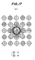
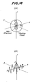
- a polaron is a freely moving conduction electron or a positive hole associated with LO-phonons or latice deformations or even more generally with electronic polarization as schematically illustrated in Fig. 17(a).
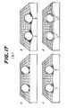
- Fig. 17(b) There is also even a concept of "bipolaron" due to coherent electronphonon intraction or electron-electron correlation effects as illustrated in Fig. 17(b).
- An exciton is an entity of elementary excitation as depicted in Fig. 18(a) which consists of a conduction electron and a positive hole bound together in an atomic hydrogen-like manner, sometimes, hybridized with (b) phonons to compose a "polariton".
- the spectral response or photoresponse signal Q(T, ⁇ ) of the curves (a) and (b) of Fig. 2 implies that there exist such parts in the specimen of Ca 2-x -Sr x -Bi 3-y -Cu y -Oz system oxide which are similar to Bi2O3 in an atomic sense, e.g., the (Bi2O2)2+ layer.
- the phenomena of optical absorption and photoconductivity of Bi2O3 have been clarified even only in part neither by experiments nor by the exciton theory. However, it is probably a typical example of Frenkel type exciton that is related to and associated with mobile charge in cation shell.
- a superconductive optoelectronic device comprises a source region, a drain region, the two regions being made of superconductive material, and a gate region made of "superconductive photoconductive-material” revealing photoconductivity at a temperature below the transition temperature of the above superconductive material.
- the invention provides an optoelectronic device with intrinsic "superconductive properties", i.e., extremely low generation rate of heat such as Joule heat during operation, and it facilitates development of various novel superconducting devices such as “an optically controllable superconductive Josephson junction devices” and “superconductive phototransistors”.
- a two-dimensional alley-like device with a high density integration of the superconductive optoelectronic devices of the invention has such electrodes and lead wire terminals which are of perfect diamagnetism, so that it is free from noises and interferences due to mutual electromagentic induction between adjacent devices or due to outside magnetic fields. Therefore, the invention enables production of an ideal "superconductive optoelectronic device or apparatus" which operates under optimal thermal and electromagentic conditions, such as a space parallel optical computer with a very high operating speed.
- the present invention is a pioneer in novel scientific field of "Superconductive Opto-Electronics”.
Abstract
Description
- This invention relates to a number of superconductive optoelectronic device and a superconductive optoelectronic apparatus. The superconductive optoelectronic devices and apparatuses of the invention are novel and vastly different from those of prior art in that the invention uses a combination of superconductive material and special superconductive photoconductive-material which reveals photoconductivity below the critical temperature of the relevant superconductive material.
- With recent development of superconductive materials, various new superconductive substances have been found; for instance, superconductive oxide materials such as those of Y-Ba-Cu-O system and Ca-Sr-Bi-Cu-O systems. However, most of current research effort are focussed on the raising of transition temperature or critical current, and not much studies except those on the reflection or scattering have been made on either optical properties of superconductive substance or industrial applications of such optical properties. The reason for it is in that, generally speaking, researchers have considered that superconductivity is incompatible with such physical properties as optical absorption and photoconductivity and they have assumed that optical irradiation in the region of an excess amount of energy with the relevant wave number beyond the energy gap of the BCS theory will merely destroy the stability of superconductivity. Further, most of the superconductive materials which have been developed so far are metals or alloys, and no superconductive materials with useful optical properties have been found. No concept has existed on a new field to be called "Superconductive Opto-Electronics"
- On the other hand, if high-temperature superconductive oxide material are combined with recently developed superconductive photoconductive-materials which reveal their proper photoconductivity at temperatures below the transition temperatures of the relevant superconductive oxide materials, a number of new electronic devices and optoelectronic apparatuses may be developed, for instance, a switching device with no power loss, an optically operating device with no power loss, an optically operating logical device, a space parallel type optically operating apparatus, a camera or an image forming device possibly with superconducting wiring, a high-speed optically operating apparatus to be driven at an extremely low power, and the like.
- Although most researchers currently aim at the raising of transition temperatures of superconductive materials, the inventor has performed a number of experiments and analyses on optical properties of superconductive oxide materials, such as those of the Y-Ba-Cu-O and La-Cu-O system, Ca-Sr-Bi-Cu-O system and Ba-Pb-Bi-O system. Consequently, the inventor has discovered an entirely new and remarkable phenomenon in that some of the above oxide materials, i.e., superconductive photoconductive-materials to be defined later, reveal onsets of photoconductivity at temperatures below the critical temperature for superconductivity (transition point) of that superconductive substance which is related to the superconductive photoconductive-material. The superconductive photoconductive-oxide materials are so far electric insulators at room temperature, but when they are cooled down to the temperatures below the transition points of superconductive materials related to them, they reveal photoconductivity, i.e., they produce photo carriers and their conductivity varies depending on the intensity of the excitation light which is incident thereto.
- A power-loss-free useful superconductive optoelectronic device can be formed by combining a superconductive photoconductive-material of for instance the Ca-Sr-Bi-Cu-O system with its related superconductive material of for instance the Ca-Sr-Bi-Cu-O system. What is meant by "superconductive optoelectronic device" is an optoelectronic device made of a combination of a superconductive material of one oxide system and that superconductive photoconductive-material of the same oxide system which reveals photoconductivity at temperatures below the critical temperatures of the superconductive material.
- An object of the invention is to provide a novel superconductive optoelectronic device by using effectively the optical properties of that superconductive photoconductive-material which is discovered by the inventor. Thus, the invention is neither a mere improvement of the prior art nor a simple solution of problems existing in the prior art, but an entirely new achievement.
- A superconductive optoelectronic device according to the present invention, for instance, comprises a substrate, a photoconductive gate region formed on the substrate, and a source region and a drain region formed on the substrate at opposite sides of the gate region respectively so as to face toward each other across the gate region. The source and drain regions are made of a superconductive material, while the gate region is made of a superconductive photoconductive-material which reveals photoconductivity at temperatures below the critical temperature for superconductivity of the superconductive material, and the superconductive photoconductive-material and the superconductive material are of the same general chemical formula but with different contents of constituent elements.
- Bias source may be connected across the source region and the drain region of the optoelectronic devices of the invention, so as to drive an electric current through its photoconductive gate region depending on the intensity of light which is incident to the photoconductive gate region.
- Once such a type of superconductive optoelectronic device is formed, it must be naturally straight forward to develop the new field from such a device to other devices, and eventually to superconductive optoelectronic apparatus, for instance a switching device with no power loss, an optically operating device with no power loss, an optically operating logical device, a space parallel type optically operating device, a camera or an image forming device possibly with superconducting wiring, a high-speed optically operating apparatus to be driven at an extremely low power, and the like.
- For a better understanding of the invention, reference is made to the accompanying drawings, in which:
- Figure 1 illustrates typical graphs showing of the temperature dependences of photoconductivity Q(T, λ) and superconductivity in resistivity ρ(T) of the Ca-Sr-Bi-Cu-O system oxides ceramics at λ≃ 580 mm and with the data of photoconductivity of the reference substance Bi₂O₃ ceramics at λ≃ 660 mm;
- Figure 2 is a graph showing the wavelength dependence of the photoconductive response Q(T, λ) of the Ca Sr Bi-Cu-O system oxides at T≃4.2K and with that of the reference substance Bi₂O₃ ceramics at T≃77K;
- Figure 3 illustrates typical graphs of the temperature dependences of photoconductivity Q(T, λ) of the Ca 1-x -Yx-Sr₂- Bi₂-Cu₂-O₂ system (X=1) oxide ceramics at λ≃660nm with the data of the photoconductivity of Q(T, λ) of the reference substance Bi₂O₃ single crystal at λ≃ 515 nm;
- Figures 4 are graphs showing the temperature dependences of resistivity in the dark of the Ca 1-x-Yx- Sr₂-Bi-Cu₂-Oz system (x=1∼0) to display an insulator to superconductor transition at x∼0.6;
- Figure 5 is a graph showing the wavelength dependences of the photoconductivity Q(T, λ) of the reference substance Bi₂O₃ single crystal at λ≃4.2K;
- Figure 6 is a graph showing the photoconductivity Q(T, λ) and superconductivity in resistivity ρ(T) of the Y3-x-Bax-Cu₃-Oz system oxides including the photoconductivity of Y₃Cu₃Oz (x=0) at λ≃480 nm and (b) Y₂Ba₁Cu₃Oz (x-1) at λ≃570 nm;
- Figure 7 is a graph showing the wavelength dependence of the photoconductive response Q(T, λ) of the Y3-x-BaxCu₃-Oz system oxides including that of Y₃Cu₃Oz (x=0) with the data of optical absorption of the reference substance Cu₂O at λ= 4.2K;
- Figure 8 is a graph to show at example of the relationship between the intensity of excitation light and photoconductive response of the Y-Ba-Cu-O system oxides Y₂Cu₃Oz (x=0) at λ≃ 470 nm;
- Figure 9 is a graph showing the temperature dependence of photoconductivity Q(T, λ) of the Ba-Pb Bi-O system oxides and at λ≃580 nm the photoconductivity of the reference substance Bi₂O₃ ceramics at λ ≃660 nm;
- Figure 10 is a graph showing the wavelength dependence of the photoconductive response Q(T, λ) of the Ba-Pb-Bi-O system oxides T≃ 4.2K and that of the reference substance Bi₂O₃ ceramics at T≃77K;
- Figure 11 is a graph showing the temperature dependence of photoconductivity Q(T, λ) and superconductivity in resistivity ρ(T) of the La-Cu-O system oxides;
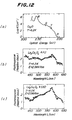
- Figure 12 is a graph showing the wavelength dependence of the photoconductive response Q(T, λ) of the semiconductive and superconductive La-Cu-O system oxides at T≃4.2K with the data of the optical abosrption of the reference substance Cu₂O at T≃4.2K;
- Figure 13 is a graph to show an example of the relationship between the intensity of excitation light and photoconductive response of La-Cu-O system oxides at λ≃570 nm;
- Figure 14 is a schematic sectional view of a superconductive optoelectronic device according to the invention;
- Figure 15 is a schematic partial sectional view of a superconductive optoelectronic alley device according to the invention;
- Figure 16 is a diagrammatic illustration of a space parallel optically operating superconductive optoelectronic apparatus which uses alleys of the superconductive optoelectronic devices of the invention;
- Figures 17 illustrate the concepts of (a) a "polaron", i.e., a conduction electron or a positive hole associated with LO-phonons or deformation of host crystal lattice together in free motion; (b) a "bipolaron" mediated via a coherent ensemble of phonons or lattice deformations;
- Figures 18 illustrate a schematic form of (a) an exciton with a wavevector K and transistion moment P, which sometimes couples with (b) photons with a wavevector η and the direction of polarization ε;
- Figures 19 are schematic diagrams to show the relationship between energy E and density of state N(E) of (a) the Ca2-x-Srx-Bi3-y-Cuy-Oz system, for the cases of x=0 (insulator) and x=1 (superconductor) and both for y=2; and (b) Ba₁-pb1-x-Bix-Oz for the cases of x≧0.35, x≃0.3, 0.2 and x<0.15; and
- Figures 20 are schematic diagrams to show the relationship between energy E and density of state N (E) of the Y3-x-Bax-Cu₃-Oz, and (b) the La₂-Cu₁-Oz systems.
- Throughout different views of the drawing in Figs. 14∼16, 1 is a substrate, 2 a gate region, 3 a source region, 4 a drain region, 5 an insulating layer, 6 a conductive glass layer, 10 an alley-like light source, 11 a coding image-mask pattern, 12 a correlative image screen, and 13 is a decoding mask optical element alley.
- The inventor's experiments and analyses on the photoconductivity and superconductivity of various superconductive materials showed that a certain portions of superconductive materials in their phase diagram reveal photoconductivity complementary to or as well as superconductivity at temperature below their regions of transition temperatures from normal conductivity to superconductivity. For instance, in the case of superconductive oxides of the Ca-Sr-Bi-Cu-O system, the inventors discovered that with changing Sr content their superconductivity can be converted into photoconductivity at temperatures below their critical temperatures.
- Figure 1 illustrates typical results of experiments on the superconductivity and photoconductivity of the Ca-Sr-Bi-Cu-O system oxides. The curve (a) in Fig. 1 shows the temperature dependence of photoconductivity of Bi₂O₃ ceramics which is a reference substance clarified by the inventor. The curve (b) in Fig. 1 illustrates the temperature dependence of superconductive photoresponse of Ca2-x-Srx-Bi₁-Cu₂-Oz (x=0). The curve (c) in Fig. 1 illustrates the temperature dependence of electric resistance of Ca2-x-Srx-Bi₁-Cu₂-Oz (x=1) in the dark. After a number of experiments and analyses on the Ca-Sr-Bi-Cu-O system oxides with a general chemical formula of Cam-x-Srx-Bin-y-Cuy-Oz, the inventors found that, under the conditions of
2≦m≦4, 3≦n≦5, 0≦x≦2, 1≦y≦3, 4≦z≦11,
if the content x of Sr is between 1 and 2, i.e., 1≦x≦2,
the oxides reveals superconductivity, while if the content x of Sr is not more than 1,i.e., 0≦x<1, the oxides reveals photoconductivity. - More particularly, with m=2, n=3, y=2 under the above-mentioned conditions, the Ca-Sr-Bi-Cu-O system reveals superconductivity if, e.g., its content x of Sr is in the range of 0.7∼1≦x≦2, and if its content x of Sr is smaller than 0.7∼1 such superconductivity disappears and it reveals complementary photoconductivity at temperature regions below their transition temperatures. Those materials whose superconductivity is converted into complementary photoconductivity and vise versa depending on the concentration of a part of their ingredient atoms at temperature regions below their transition point temperatures will be referred to as "superconductive photoconductive-materials" and their property will be referred to as "superconductive photoconductivity" herein.
- Curves (a) and (b) in Fig. 2 display wavelength dependence of photoresponse of the reference substance and the oxide specimen Bi₂O₃ ceramics at T≃77K and Ca2-x-Srx-Bi₁-Cu₂-Oz (x=0) at 4.2 K, respectively. The reference substance Bi₂O₃ ceramics and the oxide Ca2-x-Srx-Bi₁-Cu₂-Oz (x=0) have similar wavelength dependences; more specifically, as the wavelength λ decreases from 650 nm, their photoresponse Q (T, λ) gradually increases, whereas their photoresponses remain substantially at low levels for wavelengths longer than 650 nm. The inventors noted that if a material revealing photoconductivity at a temperature below its transition temperature is combined with another material revealing superconductivity at a temperature below its transition temperature, then such a combination will provide a useful superconductive optoelectronic device which reveals both superconductivity and photoconductivity at a temperature below the transition temperature thereof.
- More specifically, if an optoelectronic element of FET-like shape is formed by making a gate region with a superconductive photoconductive-material while making a source region and a drain region with a relevant superconductive material, an output current whose magnitude varies depending on the wavelength and intensity of light incident to the gate region can be produced so as to flow across the source and drain regions. If such an optoelectronic device is sustained at a temperature below the transition temperature of its superconductive material, it must work as a superconductive optoelectronic device which can be used in numerous ways; for instance, as a power-loss-free optical switching device with high-speed response, an optical detector, an optical signals amplifying device, or the like.
- In order to obtain more systematic knowledge on the characters of material systems in a series of compositions, e.g., the effect of the composition on the variations of lattice constants in a crystal structure, the inventor has studied also the (Ca1-xYx)Sr₂Bi₂Cu₂Oz system to obtain data especially from the view point of photoconductivity complementary to superconductivity together with new data of the reference substance Bi₂O₃ single crystals. [Characteristic features of this series of system such as the variations of lattice constants, electrical resistivity in the dark and a magnetic susceptibility with varying x have been studied in details by T. Tamegai et al. Jpn. J. Appln. Phys. 27 L1074 (1988) and T. Tamegai, Parity Vol.3, No. 11, 43 06 (1988) (in Japanese).] The single crystals of Bi₂O₃ have been grown for the first time in the inventor's laboratory.
- Figure 3(a) and (b) illustrate typical traces of the temperature dependences of photoconductivity signals Q (T, λ) of the reference substance Bi₂O₃ single crystal and of the Ca1-xYxSr₂Bi₂Cu₂Oz (x=1) specimen of oxide Ceramics, whereas Fig. 4(a) and (b) show the temperature dependences of resistivity in the dark of the Ca1-xYxSr₂Bi₂Cu₂Oz System (x=1∼0) to display an insulator to superconductor transition between x≃ 0.55 and x≃0.6.
- With these data, one can definitely recognize even another more systematic series of material Ca1-xYxSr₂Bi₂Cu₂Oz also exhibits an emergence of superconductive photoconductivity at x≃ 1, but rather low temperature T≃20K. In Fig. 5, the graph displays the wavelength dependences of the photoconductivity Q (T, λ) of the reference substance Bi₂O₃ single crystal. This is not necessarily inconsistent with the data in Fig. 2(a), since thickness of specimens and proportion of the surface to volume ratio are different from each other.
- Oxide material of the Y-Ba-Cu-O system will be described now by referring to Fig. 6 which shows test results on its superconductivity and photoconductivity. The curve (a) in Fig. 6 shows the temperature dependence of photoresponse Q (T, λ) of Y3-x-Bax-Cu₃-Oz (x=0), the curve (b) shows the temperature dependence of photo-response Q (T, λ) of Y3-x-Bax-Cu₃-Oz (x=1), and curves (c) in Fig. 3 show the temperature dependence of dark resistivity of two specimens of Y3-x-Bax-Cu₃-Oz (x=1, x=2). In the case of Y-Ba-Cu-O system oxides with a general chemical formula of Y3-x-Bax-Cuy-Oz , their superconductivity is converted into photoconductivity depending on both the content x of Ba and the content z of oxygen. Under the conditions of
1≦x≦2 and 6.5≦z≦7,
the oxides reveal superconductivity, while under the conditions of
0≦x≦1 and 7.0≦z≦7.5, or x=2 and 6.0≦z<6.5,
the oxides reveal photoconductivity at temperatures below their transition temperatures. Here, z< 6.5 is a merely rough indication of the boundary not clearly and should not be taken exactly, since the superconductive defined photoconductive-area are continuously close to the superconductive-areas in thier phase diagram. Similar situations are the cases also for the other systems as far as the oxygen content z concerns. - As can be seen from the curves (a) and (b) in Fig. 6, the two specimens of Y3-x-Bax-Cu₃-Oz (x=0, x=1) clearly reveal superconductive photoconductivity at temperatures below their transition temperatures.
- Fig. 7 shows the dependence of photoconductivity Q(T, λ) of the above Y-Ba-Cu-O system oxides on the wavelength λ of excitation light at a temperature T=79 K. As can be seen from Fig. 7, the oxides reveal intrinsic photoconductivity at a temperature below their transition temperatures in response to excitation light with wavelength at λ=420-640 nm. Fig. 8 shows the dependence of the photoconductivity of the similar oxide (x=0) system on the intensity of excitation light at a wavelength λ=470 nm. It may be concluded from Fig. 8 that photoresponse signals Q (T, λ) of the oxide material of Y3-x-Bax-Cu₃-Oz system increases with the intensity of the excitation light. The inventors found that the Y3-x-Bax-Cu₃-Oz system oxide becomes a superconductive photoconductive-material when its Ba concentration x is in a
range 0≦x≦1, while it becomes a superconductive material for 1≦x≦2. - Oxide material of Ba-Pb-Bi-O system will be described now by referring to Fig. 9 and Fig. 10. Curves (a) and (b) in Fig. 9 show the temperature dependences of photoresponse Q (T, λ) of a reference substance Bi₂O₃ ceramics and oxide specimens with a general chemical formula of Ba₁-Pb1-x-Bix Oz, respec tively. Curves (a) and (b) in Fig. 10 show the wavelength dependences of such photoresponse Q (T, λ) of the reference substance Bi₂O₃ ceramics and the above specimens Ba₁-Pb1-x-Bix-Oz (x=0.5), respectively. In the case of the oxides with a general chemical formula of Ba₁-Pb1-x-Bix-Oz, the inventor found that they reveal superconductivity under the conditions of
0.20≦x≦0.35 and 2.81≦z≦3,
while they reveal photoconductivity under the conditions of
x≧0.35 and 2.7≦z≦2.81. - Referring to Fig. 11 through Fig. 13, oxide material of the La₂-Cu₁-Oz system will be described now. Curves (a) and (b) in Fig. 11 show the temperature dependence of photoresponse Q (T, λ) of the oxide for cases of z=3.88 and z=3.92, respectively. Curve (c) in Fig. 11 shows the temperature dependence of resistance of the oxide in the dark for both z=3.88 and z=3.92. It has been known that La₂-Cu₁-Oz system oxide with z≧3.92 reveals superconductivity at a temperature below about 30 K. The inventors found that if the oxygen concentration of such oxide is reduced, its superconductivity is converted into photoconductivity as shown in Fig. 11. It was also found that the oxide reveals photoconductivity over a wavelength range of λ≃450-650 nm as shown by curve (b) (for z=3.88) and curve (c) for (z≃3.92) in Fig. 9. Fig. 13 shows the relationship between the photoconductivity and the quantity of incident light (i.e., excitation light intensity) for the above oxide with z≃3.88. It can be seen from Fig. 13 that the photoresponse current clearly increases with the intensity of incident light.
- Fig. 14 is a schematic diagram showing the structure of an embodiment of the superconductive optoelectronic device according to the invention. The embodiment is a superconductive phototransistor in which a positive gate voltage VG is used (VG≧0). A
substrate 1 is made of SrTiO₃, and aphotoconductive gate region 2 is formed on thesubstrate 1 with superconductive photoconductive-material Ca₂-Bi₁-Cu₂-Oz. Thephotoconductive gate region 2 has a width of 0.2 µm to 1.0 mm and a thickness of 1-10 µm. The above superconductive photoconductive-material Ca₂-Bi₁-Cu₂-Oz reveals photoconductivity in response to excitation by incident light of wavelength at least λ≃540-740 nm at a temperature below the transition temperature of a superconductive substance Ca₁-Sr₁-Bi₁-Cu₂-Oz. At opposite portions over thegate region 2, asource region 3 and adrain region 4 are formed with Ca₁-Sr₁- Bi₁-Cu₂-Oz oxide which reveals superconductivity below its critical temperature of 80K or 105-115 K. An electrically insulatinglayer 5 which is optically transparent is formed so as to cover top surfaces of thegate resion 2, thesource region 3, and thedrain region 4. The insulatinglayer 5 of the illustrated example was a 1 µm thick SiO₂ film or mylar sheet. Further, a conductive surface ofglass layer 6, for instance made of a NESA (Trademark of Pittsburgh Plate Glass Company) glass layer, is placed on the insulatinglayer 5, and electrodes are deposited on the conductive surface ofglass layer 6. - A source for bias voltage VG is connected across the
source region 3 and electrodes of the conductive surface of glass layer and a source for source-drain voltage VSD is connected between thesource region 3 and thedrain region 4 across thegate region 2. - In preparation of the
source region 3 and thedrain region 4, it is also possible even to form a comparatively broad region of Ca2-x Srx Bi₁-Cu₂-Oz (x=0) at first and then change continuously the concentrations of Ca and Sr so as to produce a gradual concentration change from x=0 to x=1 in the broad region only at both sides. - In operation, the superconducting optoelectronic element of Fig. 14 is cooled to a temperature below the critical temperatures, i.e., about 80K or 105-115K, of the superconducting zones of Ca2-x-Srx-Bi₁-Cu₂-Oz and excitation light signals in a wavelength range is irradiated to the
gate region 2. A pulsed dye ;aser of 3 nsec width can be used for an excitation light source. This fact basically indicates a high speed response of the device itself. Thereby, photocarriers are generated in thegate region 2 depending on the photon number or intensity of light incident thereto. The generated carriers are accelerated by the source-drain voltage VSD so as to produce an induced output current which is delivered to an output resistor R. Accordingly, an output voltage due to incident photosignals appears across the resistor R. - The amount and density of optically excited carriers in the
gate region 2 can be variable depending not only on the photon number or intensity of incident light thereto but also the bias voltage VG, and the bias voltage VG can be harmoniously adjusted so as to meet specific requirements from users . By selecting an appreciate wavelength λ for excitation light, photocarrier density of the order, e.g., of 10¹²/cm³ can be obtainable in a surface layer of thegate region 2. With the above output current characteristics depending on the intensity of incident light, the superconducting optoelectronic device of Fig. 14 can be used as a superconductive switching device. Thesource region 3 and thedrain region 4 made of superconductive material are free from heat generation during operation, so that the optoelectronic device of Fig. 14 possesses those advantages which are inherent to superconductivity. - Fig. 15 is a partial schematic diagram of an embodiment of the superconductive optoelectronic device of the invention, in which device a number of the superconductive optoelectronic devices of Fig. 16 are integrated at a high density in the form of one- or two-dimensional alleys. If wiring among different devices in the device of Fig. 15 is made by using superconducting material, heat generation in the alley or apparatus can be suppressed to an extremely low level.
The superconducting optoelectronic device and apparatus of the invention can be used in various fields; for instance, as a loss free pick up (or camera) devices, loss-free detectors of optical signals in an optical computer which executes parallel operations in a spatially arranged manner, and the like. The device of the invention can be also used in a multiple channel system which selectively utilizes a number of different wavelengths in the incident light. - Fig. 16 schematically illustrates an optical calculation procedure in a projection-correlative optical system of a space parallel optical computer in which system the superconductive optoelectronic devices of the invention are used. As alley-like
light source 10 projects a number of optical signals in parallel onto a coding mask pattern 11. The mask pattern 11 carries coding image signals in a mask fashion, which signals correspond to the type of operation to be superposed to the light beams. After passing through the mask pattern 11, the light beams pass acorrelative image screen 12 and then enter in parallel into the corresponding devices in a decoding maskoptical device alley 13. Each optical device receives a coded signal which is modulated by the mask screen, and operated results can be obtained from the optoelectronic output signals from each of the optical devices. If each optical device of the decoding maskoptical device alley 13 is the superconductive optoelectronic device of the invention, parallel optical operations can be effected while minimizing heat generation during the operation. - Although the invention has been described so far by referring to an embodiment in the form of three-terminal device, the superconductive optoelectronic device of the invention can be also made in the form of a two-terminal device. More particularly, carriers generated under the condition of VG=0 in a broad gate region are influenced by the superconductive proximity effect due to superconductive photoconductivity irrespective of a small coherence length, and one can expect that the superconductive optoelectronic device of the invention may be used as a superconductive Josephson junction device based on light irradiation. Thus, such two-terminal device may be treated as a "superconductive photoconductivity or optically controlled Josephson junction device". In this case, the gate width and the intensity of the incident light must be properly selected.
- The illustrated embodiment of the invention is made by using the Ca-Sr-Bi-Cu-O system oxides, but other superconductive photoconductive-materials such as those of the Ba-Pb-Bi-O system, La-Cu-O system, or Y-Ba-Cu-O system can be also used to form the superconducting optoelectronic device and apparatus of the invention. For instance, a superconducting optoelectronic device which is similar to the embodiment of Fig. 14 can be made by forming the gate region with Ba₁-Pb0.5-Bi0.5-O₃, while forming the source region and the drain region with Ba₁-Pb0.75-Bi0.25-O₃.
- The detailed mechanism of the above photoconductive phenomenan of the superconductive photoconductive materials have not been fully clarified yet, but the inventor assumes it on the basis of the concepts of "polarons and excitions as follows. A polaron is a freely moving conduction electron or a positive hole associated with LO-phonons or latice deformations or even more generally with electronic polarization as schematically illustrated in Fig. 17(a). There is also even a concept of "bipolaron" due to coherent electronphonon intraction or electron-electron correlation effects as illustrated in Fig. 17(b).
- An exciton is an entity of elementary excitation as depicted in Fig. 18(a) which consists of a conduction electron and a positive hole bound together in an atomic hydrogen-like manner, sometimes, hybridized with (b) phonons to compose a "polariton".
- The spectral response or photoresponse signal Q(T, λ) of the curves (a) and (b) of Fig. 2 implies that there exist such parts in the specimen of Ca2-x-Srx-Bi3-y-Cuy-Oz system oxide which are similar to Bi₂O₃ in an atomic sense, e.g., the (Bi₂O₂)²⁺ layer. The phenomena of optical absorption and photoconductivity of Bi₂O₃ have been clarified even only in part neither by experiments nor by the exciton theory. However, it is probably a typical example of Frenkel type exciton that is related to and associated with mobile charge in cation shell. The positions of the fine structures in the Q(λ, T) in Fig. 2 basically coincide with those of the fundamental absorption edge in Bi₂O₃ itself. We can recognize a few prominent fine structures probably due to the excitons, e.g., structures around λ≃623 nm in the photoconductivity spectra of Ca₂-Bi₁-Cu₂-O₃ similar to those of Bi₂O₃ ceramics structure of which appear to correspond to the n=2 state in a certain series of excitons of Bi₂O₃. Thus, we may reasonably conceive that there exists at least a finite fraction of the Bi₂O₃-like part or phase which cannot be ignored in the Ca-Sr-Bi-Cu-O system substance, where the photoexcited electrons and holes are definitely mobile, irrespective of a certain difference of the crystal structures and the density of states. (See Fig. 19 (a))
- A conduction electron or a positive hole in standard types of Bi₂O₃ or Cu₂O crystals has been reported to form a rather small or large polaron, respectively. However, an onset of "photoconductivity" Q(λ, T) even in the insulating specimens is clearly associated with an onset of "superconductivity" as if the superconductivity potentially underlies the photoconductivity phenomenon or vice versa. Thus, as to the effects of a polaron, whether it is a large polaron due to interaction with the LO-phonons, a small one due to the Jahn-Teller effect or possibly an intermediate one due to both effects, the effects of a polaron must be at least potentially important as indicated in Fig. 1 through Fig. 13, as well as "the electronically polarized polaron effect". They are probably effective in a coherently hybridized form of elementary excitations. Here, we must pay special attention to the electronically polarized polarons, which one may call an "excitonic polaron". No one can fail to recognize close association among polarons and excitons with the experimental data here.
- As shown in Fig. 19 (a), these polarons and excitons in the Ca Sr-Bi-Cu-O system had yielded out of the optical interband transition from the hybridized oxygen-(2p) and Bi-(6s) valence bands mainly to the Bi-(6p) conduction band together with the LO-phonon interaction, while leaving O(2p)⁶Bi(6s)¹ "holes" (represented by a white circle) and creating a Bi(6p)¹ conduction electron. However, a polaron in the Ca-Sr-Bi-Cu-O system substance can be created either by the optical excitation or substitution of Ca with Sr perhaps via a chemical pressure. (See Fig. 19 (a) x=0 and (b) x=1). In this case, the substance becomes superconductive at x=1.) Since the positive holes in the hybrid Bi(6s) and O(2p) bands can be created from the many-body ground state by either an intra- or interband transition, the electron correlation effects naturally important. One must pay more attention to the dynamical valence fluctuation between Bi³⁺ and Bi⁵⁺ and especially between Cu¹⁺and Cu²⁺, as well as between Bi³⁺ and Bi⁴⁺ and between Cu²⁺ and Cu³⁺. Therefore, for the mechanism of high-temperature superconductivity, we may reasonably conceive potential roles of an ensemble of polarons, whether large or small, and especially closely associated excitons. The ensemble of united polarons and excitons here are probably a set of bipolarons, polaronic excitons and/or, most probably, "exciton-mediated bipolarons" due to the dynamical electronphonon and electron correlation effects.
- The photoresponse signals Q(T, λ) of Ca-Sr-Bi-Cu-O system substance as depicted by the curve (b) in Fig. 2 are very similar to those of Bi₂O₃ ceramics of the curve (a) in Fig. 2. Consequently, we believe that these studies of elementary excitations here must reveal the nature of superconducting ground state, irrespective of an enormous difference in carrier density. In both, the an excited state via elementary excitation (insulator) in Fig. 19 (a) and the ground state (superconductor) in Fig. 19 (b), one can expect occurrence of similar phenomena to those of the Josephson effect. Similar situations must be the cases also for the Ba-Pb-Bi-O, Y-Cu-O, Y-Ba-Cu-O, La-Cu-O systems but with other reasoning as suggested in Fig. 19(b) and Figs. 20(a) and (b).
- To the best of our knowledge, this is the first clear experimental indication of the polaron and exciton mechanisms displayed in the high-temperature super conductivity of Ca-Sr-Bi-Cu-O, Ca(Y)-Sr-Bi-Cu-O, Y-Cu-O, Y-Ba-Cu-O, Ba-Pb-Bi-O, and La-Cu-O system substances.
- As described in detail in the foregoing, a superconductive optoelectronic device according to the invention comprises a source region, a drain region, the two regions being made of superconductive material, and a gate region made of "superconductive photoconductive-material" revealing photoconductivity at a temperature below the transition temperature of the above superconductive material. Thus, the invention provides an optoelectronic device with intrinsic "superconductive properties", i.e., extremely low generation rate of heat such as Joule heat during operation, and it facilitates development of various novel superconducting devices such as "an optically controllable superconductive Josephson junction devices" and "superconductive phototransistors".
- Further, a two-dimensional alley-like device with a high density integration of the superconductive optoelectronic devices of the invention has such electrodes and lead wire terminals which are of perfect diamagnetism, so that it is free from noises and interferences due to mutual electromagentic induction between adjacent devices or due to outside magnetic fields. Therefore, the invention enables production of an ideal "superconductive optoelectronic device or apparatus" which operates under optimal thermal and electromagentic conditions, such as a space parallel optical computer with a very high operating speed.
- In short, the present invention is a pioneer in novel scientific field of "Superconductive Opto-Electronics".
- Although the invention has been described with a certain degree of particularity, it must be understood that the present disclosure has been made only by way of example and that numerous variations in details may be resorted to without departing from the scope of the invention as hereinafter claimed.
Claims (6)
0≦x≦1, y=3, 7.0≦z≦7.5,
and said source region and said drain region are made of a superconductive material having a general chemical formula of Y3-x-Bax-Cuy-Oz with numbers of atom of
1≦x≦2, y=3, 6.5≦z≦7.
x=2, y=3, 6.0≦z≦6.5,
and said source region and said drain zone are made of a superconductive material having a general chemical formula of Y3-x-Bax-Cuy-Oz with numbers of atom of
1≦x≦2, y=3, 6.5≦z≦7.
3.86≦z≦3.92,
and said source region and said drain region are made of a superconductive material having a general chemical formula of La₂-Cu₁-Oz with a number of atom of
3.92≦z≦4.02.
2≦m≦4, 0≦x≦2, 3≦n≦5, 1≦y≦3, 4≦z≦11,
and said source region and said drain region are made of a superconductive material having a general chemical formula Cam-x-Srx-Bin-y-Cuy-Oz of with number of atom of
2≦m≦4, 1≦x≦2, 3≦n≦5, 1≦y≦3, 4≦ z≦11.
0.35≦x, 2.7≦ z≦3,
and said source region and said drain region are made of a superconductive material having a general chemical formula Ba₁-Pb1-x-Bix-Oz of with numbers of atom of
0.2≦x≦0.35, 2.81 ≦z≦3.
Applications Claiming Priority (4)
| Application Number | Priority Date | Filing Date | Title |
|---|---|---|---|
| JP57844/88 | 1988-03-11 | ||
| JP5784488 | 1988-03-11 | ||
| JP201655/88 | 1988-08-12 | ||
| JP63201655A JPH01315177A (en) | 1988-03-11 | 1988-08-12 | Superconductive optoelectronic element and device thereof |
Publications (3)
| Publication Number | Publication Date |
|---|---|
| EP0332448A2 true EP0332448A2 (en) | 1989-09-13 |
| EP0332448A3 EP0332448A3 (en) | 1989-11-23 |
| EP0332448B1 EP0332448B1 (en) | 1996-05-15 |
Family
ID=26398929
Family Applications (1)
| Application Number | Title | Priority Date | Filing Date |
|---|---|---|---|
| EP89302357A Expired - Lifetime EP0332448B1 (en) | 1988-03-11 | 1989-03-09 | Superconductive optoelectronic devices |
Country Status (4)
| Country | Link |
|---|---|
| US (1) | US4990487A (en) |
| EP (1) | EP0332448B1 (en) |
| CA (1) | CA1310391C (en) |
| DE (1) | DE68926471T2 (en) |
Cited By (21)
| Publication number | Priority date | Publication date | Assignee | Title |
|---|---|---|---|---|
| EP0456513A2 (en) * | 1990-05-11 | 1991-11-13 | The University of Tokyo | Superconductive optoelectronic device with Cu20 as photoconductive material |
| EP0469922A2 (en) * | 1990-08-03 | 1992-02-05 | The University of Tokyo | Superconductive optoelectronic devices with the basic substance Bi203 of superconductive-conjugate photoconductivity |
| EP0523937A1 (en) * | 1991-07-16 | 1993-01-20 | The University of Tokyo | Photoconductive substances of the bismuth-strontium-calcium-lanthanum-yttrium-copper-oxygen system |
| EP1427028A1 (en) * | 2001-09-14 | 2004-06-09 | National Institute of Advanced Industrial Science and Technology | ULTRA HIGH−SPEED PHOTOELECTRIC SIGNAL CONVERSION ELEMENT |
| EP1715055A2 (en) | 2005-04-22 | 2006-10-25 | Degussa GmbH | Process for the production of L-amino acids using improved Enterobacteriaceae strains |
| DE102007051024A1 (en) | 2007-03-05 | 2008-09-11 | Evonik Degussa Gmbh | Process for the preparation of L-amino acids using strains of the family Enterobacteriaceae |
| EP1975241A1 (en) | 2007-03-29 | 2008-10-01 | Evonik Degussa GmbH | Method for manufacturing L-amino acids using improved strains of the enterobacteriaceae family |
| EP2036979A1 (en) | 2007-09-15 | 2009-03-18 | Evonik Degussa GmbH | Method for manufacturing L-amino acids using improved strains of the enterobacteriaceae family |
| EP2055785A1 (en) | 2007-11-02 | 2009-05-06 | Evonik Degussa GmbH | Method for manufacturing L-amino acids using improved strains of the enterobacteriaceae family |
| EP2060636A1 (en) | 2007-11-14 | 2009-05-20 | Evonik Degussa GmbH | Method for manufacturing L-amino acids using improved strains of the enterobacteriaceae family |
| EP2098597A1 (en) | 2008-03-04 | 2009-09-09 | Evonik Degussa GmbH | Method for manufacturing L-amino acids using improved strains of the enterobacteriaceae family |
| DE102008002309A1 (en) | 2008-06-09 | 2009-12-10 | Evonik Degussa Gmbh | Process for the preparation of L-amino acids using improved strains of the family Enterobacteriaceae |
| DE102008040352A1 (en) | 2008-07-11 | 2010-01-14 | Evonik Degussa Gmbh | Process for the preparation of L-tryptophan using improved strains of the family Enterobacteriaceae |
| DE102008044768A1 (en) | 2008-08-28 | 2010-03-04 | Evonik Degussa Gmbh | Process for the preparation of organochemical compounds using improved strains of the family Enterobacteriaceae |
| WO2010149574A1 (en) | 2009-06-25 | 2010-12-29 | Evonik Degussa Gmbh | Method for fermentatively preparing l-amino acids |
| EP2267145A1 (en) | 2009-06-24 | 2010-12-29 | Evonik Degussa GmbH | Method for manufacturing L-amino acids using improved strains of the enterobacteriaceae family |
| WO2011124477A2 (en) | 2010-03-30 | 2011-10-13 | Evonik Degussa Gmbh | METHOD FOR THE PRODUCTION OF L-ORNITHINE USING BACTERIA THAT OVEREXPRESS LysE |
| DE102011006716A1 (en) | 2011-04-04 | 2012-10-04 | Evonik Degussa Gmbh | Microorganism and process for the fermentative production of an organic chemical compound |
| EP2762571A1 (en) | 2013-01-30 | 2014-08-06 | Evonik Industries AG | Microorganism and method for the production of amino acids by fermentation |
| EP3608409A1 (en) | 2018-08-09 | 2020-02-12 | Evonik Operations GmbH | Process for preparing l amino acids using improved strains of the enterobacteriaceae family |
| DE102020213681A1 (en) | 2020-10-30 | 2022-05-05 | Forschungszentrum Jülich GmbH | Electroluminescence of ceramic materials |
Families Citing this family (10)
| Publication number | Priority date | Publication date | Assignee | Title |
|---|---|---|---|---|
| US5168165A (en) * | 1988-02-04 | 1992-12-01 | The University Of Tokyo | Superconductive photoconductive-substance of the Y-Ba-Cu-O system and a method for producing the same |
| US5219831A (en) * | 1988-02-04 | 1993-06-15 | University Of Tokyo | Superconductive photoconductive-substance of the La-Cu-O system and a method for producing the same |
| JPH06102549B2 (en) * | 1988-08-12 | 1994-12-14 | 東京大学長 | Ca-Sr-Bi-Cu-O-based oxide superconducting photoconductive material and method for producing the same |
| JPH06102548B2 (en) * | 1988-08-12 | 1994-12-14 | 東京大学長 | Ba-Pb-Bi-O-based oxide superconducting photoconductive material and method for producing the same |
| DE69009109T2 (en) * | 1989-07-05 | 1994-09-15 | Canon Kk | Device and method for measuring light. |
| JP2503091B2 (en) * | 1990-03-14 | 1996-06-05 | 富士通株式会社 | Superconducting light guide function element |
| US5116807A (en) * | 1990-09-25 | 1992-05-26 | The United States Of America As Represented By The Administrator Of The National Aeronautics And Space Administration | Monolithic MM-wave phase shifter using optically activated superconducting switches |
| US5328893A (en) * | 1991-06-24 | 1994-07-12 | Superconductor Technologies, Inc. | Superconducting devices having a variable conductivity device for introducing energy loss |
| US5768002A (en) * | 1996-05-06 | 1998-06-16 | Puzey; Kenneth A. | Light modulation system including a superconductive plate assembly for use in a data transmission scheme and method |
| US20100013559A1 (en) * | 2007-02-02 | 2010-01-21 | Max Lee B | High frequency amplifying device |
Family Cites Families (10)
| Publication number | Priority date | Publication date | Assignee | Title |
|---|---|---|---|---|
| NL286177A (en) * | 1961-12-01 | |||
| US4464065A (en) * | 1982-08-09 | 1984-08-07 | The United States Of America As Represented By The Secretary Of The Navy | Fast granular superconducting bolometer |
| JPS6065582A (en) * | 1983-09-20 | 1985-04-15 | Nippon Telegr & Teleph Corp <Ntt> | Grain boundary josephson junction photodetector |
| DE3373167D1 (en) * | 1983-12-28 | 1987-09-24 | Ibm | Low temperature tunneling transistor |
| JPS60253929A (en) * | 1984-05-31 | 1985-12-14 | Shimadzu Corp | Infrared image sensor |
| JPS61271487A (en) * | 1985-05-27 | 1986-12-01 | Masahiko Kurakado | Radiation using superconductive tunnel junction and light incident position detector |
| US4843446A (en) * | 1986-02-27 | 1989-06-27 | Hitachi, Ltd. | Superconducting photodetector |
| JPS63241809A (en) * | 1987-03-27 | 1988-10-07 | Sumitomo Electric Ind Ltd | Transparent conductor |
| JPS63245973A (en) * | 1987-03-31 | 1988-10-13 | Sumitomo Electric Ind Ltd | Superconducting element |
| US4814598A (en) * | 1987-09-03 | 1989-03-21 | Hypres, Inc. | Optical wavelength analyzer and image processing system utilizing Josephson junctions |
-
1989
- 1989-03-07 US US07/320,131 patent/US4990487A/en not_active Expired - Lifetime
- 1989-03-08 CA CA000593077A patent/CA1310391C/en not_active Expired - Lifetime
- 1989-03-09 DE DE68926471T patent/DE68926471T2/en not_active Expired - Fee Related
- 1989-03-09 EP EP89302357A patent/EP0332448B1/en not_active Expired - Lifetime
Non-Patent Citations (4)
| Title |
|---|
| APPLIED PHYSICS LETTERS, vol. 43, no. 3, 1st August 1983, pages 314-316, American Institute of Physics, New York, US; M. ITO et al.: "Highly sensitive photodetection using a microwave-coupled BaPb0.7Bi0.3O3 Josephson junction array" * |
| APPLIED PHYSICS LETTERS, vol. 51, no. 24, 14th December 1987, pages 2046-2047, American Institute of Physics, Tokyo, JP; M. LEUNG et al.: "Optical detection in thin granular films of Y-Ba-Cu-O at temperatures between 4.2 and 100 K" * |
| JAPANESE JOURNAL OF APPLIED PHYSICS, vol. 24, no. 24-2, 1985, pages 471-473, "Proceedings of the sixt international meeting on ferroelectricity", Kobe, JP; Y. ENOMOTO et al.: "Optical detector using superconducting BaPb0.7Bi0.3O3 (BPB) thin films" * |
| JOURNAL OF APPLIED PHYSICS, vol. 59, no. 11, 1st June 1987, pages 3807-3814, American Institute of Physics, New York, US; Y. ENOMOTO et al.: "Optical detector using superconducting BaPb0.7Bi0.3O3 thin films" * |
Cited By (39)
| Publication number | Priority date | Publication date | Assignee | Title |
|---|---|---|---|---|
| EP0456513A2 (en) * | 1990-05-11 | 1991-11-13 | The University of Tokyo | Superconductive optoelectronic device with Cu20 as photoconductive material |
| EP0456513A3 (en) * | 1990-05-11 | 1992-02-19 | University Of Tokyo | Superconductive optoelectronic device with the basic substance cu20 of superconductive-conjugate photoconductivity |
| US5244870A (en) * | 1990-05-11 | 1993-09-14 | The University Of Tokyo | Superconductive optoelectronic device with the basic substance Cu2 O of superconductive-conjugate photoconductivity |
| EP0469922A2 (en) * | 1990-08-03 | 1992-02-05 | The University of Tokyo | Superconductive optoelectronic devices with the basic substance Bi203 of superconductive-conjugate photoconductivity |
| EP0469922A3 (en) * | 1990-08-03 | 1992-06-03 | University Of Tokyo | Superconductive optoelectronic devices with the basic substance bi203 of superconductive-conjugate photoconductivity |
| US5462916A (en) * | 1990-08-03 | 1995-10-31 | The University Of Tokyo | Superconductive optoelectronic devices with the basic substance Bi2 O3 of superconductive-conjugate photoconductivity |
| EP0523937A1 (en) * | 1991-07-16 | 1993-01-20 | The University of Tokyo | Photoconductive substances of the bismuth-strontium-calcium-lanthanum-yttrium-copper-oxygen system |
| US5445766A (en) * | 1991-07-16 | 1995-08-29 | The University Of Tokyo | Superconductive conjugate photoconductive substances of the Bi-SrCa(LaY)-Cu-O system, a method for producing the same and superconductive optoelectronic devices using the same |
| US5654259A (en) * | 1991-07-16 | 1997-08-05 | The University Of Tokyo | Superconductive conjugate photoconductive substances of the Bi-SrCa (laY)-Cu-O system, a method for producing the same and superconductive optoelectronic devices using the same |
| EP1427028A4 (en) * | 2001-09-14 | 2009-08-12 | Nat Inst Of Advanced Ind Scien | Ultra high-speed photoelectric signal conversion element |
| EP1427028A1 (en) * | 2001-09-14 | 2004-06-09 | National Institute of Advanced Industrial Science and Technology | ULTRA HIGH−SPEED PHOTOELECTRIC SIGNAL CONVERSION ELEMENT |
| EP1715055A2 (en) | 2005-04-22 | 2006-10-25 | Degussa GmbH | Process for the production of L-amino acids using improved Enterobacteriaceae strains |
| DE102007051024A1 (en) | 2007-03-05 | 2008-09-11 | Evonik Degussa Gmbh | Process for the preparation of L-amino acids using strains of the family Enterobacteriaceae |
| EP1975241A1 (en) | 2007-03-29 | 2008-10-01 | Evonik Degussa GmbH | Method for manufacturing L-amino acids using improved strains of the enterobacteriaceae family |
| EP2036979A1 (en) | 2007-09-15 | 2009-03-18 | Evonik Degussa GmbH | Method for manufacturing L-amino acids using improved strains of the enterobacteriaceae family |
| DE102007044134A1 (en) | 2007-09-15 | 2009-03-19 | Evonik Degussa Gmbh | Process for the preparation of L-amino acids using improved strains of the family Enterobacteriaceae |
| EP2465869A1 (en) | 2007-11-02 | 2012-06-20 | Evonik Degussa GmbH | Method for manufacturing L-amino acids using improved strains of the enterobacteriaceae family |
| EP2055785A1 (en) | 2007-11-02 | 2009-05-06 | Evonik Degussa GmbH | Method for manufacturing L-amino acids using improved strains of the enterobacteriaceae family |
| DE102007052270A1 (en) | 2007-11-02 | 2009-05-07 | Evonik Degussa Gmbh | Process for the preparation of L-amino acids using improved strains of the family Enterobacteriaceae |
| EP2060636A1 (en) | 2007-11-14 | 2009-05-20 | Evonik Degussa GmbH | Method for manufacturing L-amino acids using improved strains of the enterobacteriaceae family |
| EP2098597A1 (en) | 2008-03-04 | 2009-09-09 | Evonik Degussa GmbH | Method for manufacturing L-amino acids using improved strains of the enterobacteriaceae family |
| DE102008002309A1 (en) | 2008-06-09 | 2009-12-10 | Evonik Degussa Gmbh | Process for the preparation of L-amino acids using improved strains of the family Enterobacteriaceae |
| EP2133420A1 (en) | 2008-06-09 | 2009-12-16 | Evonik Degussa GmbH | Method for manufacturing L-amino acids using improved strains of the enterobacteriaceae family |
| DE102008040352A1 (en) | 2008-07-11 | 2010-01-14 | Evonik Degussa Gmbh | Process for the preparation of L-tryptophan using improved strains of the family Enterobacteriaceae |
| EP2147972A1 (en) | 2008-07-11 | 2010-01-27 | Evonik Degussa GmbH | Method for manufacturing L-tryptophane using improved strains of the enterobacteriaceae family |
| DE102008044768A1 (en) | 2008-08-28 | 2010-03-04 | Evonik Degussa Gmbh | Process for the preparation of organochemical compounds using improved strains of the family Enterobacteriaceae |
| EP2163613A2 (en) | 2008-08-28 | 2010-03-17 | Evonik Degussa GmbH | Method for manufacturing organic chemical compounds using improved strains of the enterobacteriaceae family |
| EP2267145A1 (en) | 2009-06-24 | 2010-12-29 | Evonik Degussa GmbH | Method for manufacturing L-amino acids using improved strains of the enterobacteriaceae family |
| DE102009030342A1 (en) | 2009-06-25 | 2010-12-30 | Evonik Degussa Gmbh | Process for the fermentative production of organic chemical compounds |
| WO2010149574A1 (en) | 2009-06-25 | 2010-12-29 | Evonik Degussa Gmbh | Method for fermentatively preparing l-amino acids |
| WO2011124477A2 (en) | 2010-03-30 | 2011-10-13 | Evonik Degussa Gmbh | METHOD FOR THE PRODUCTION OF L-ORNITHINE USING BACTERIA THAT OVEREXPRESS LysE |
| DE102010003419A1 (en) | 2010-03-30 | 2012-04-12 | Evonik Degussa Gmbh | Process for the fermentative production of L-ornithine |
| DE102010003419B4 (en) | 2010-03-30 | 2019-09-12 | Evonik Degussa Gmbh | Process for the fermentative production of L-ornithine |
| DE102011006716A1 (en) | 2011-04-04 | 2012-10-04 | Evonik Degussa Gmbh | Microorganism and process for the fermentative production of an organic chemical compound |
| WO2012136506A2 (en) | 2011-04-04 | 2012-10-11 | Evonik Degussa Gmbh | Microorganism and processes for the fermentative production of an organo-chemical compound |
| EP2762571A1 (en) | 2013-01-30 | 2014-08-06 | Evonik Industries AG | Microorganism and method for the production of amino acids by fermentation |
| WO2014117992A1 (en) | 2013-01-30 | 2014-08-07 | Evonik Industries Ag | Microorganism and method for production of amino acids by fermentation |
| EP3608409A1 (en) | 2018-08-09 | 2020-02-12 | Evonik Operations GmbH | Process for preparing l amino acids using improved strains of the enterobacteriaceae family |
| DE102020213681A1 (en) | 2020-10-30 | 2022-05-05 | Forschungszentrum Jülich GmbH | Electroluminescence of ceramic materials |
Also Published As
| Publication number | Publication date |
|---|---|
| DE68926471T2 (en) | 1996-11-28 |
| DE68926471D1 (en) | 1996-06-20 |
| US4990487A (en) | 1991-02-05 |
| EP0332448A3 (en) | 1989-11-23 |
| CA1310391C (en) | 1992-11-17 |
| EP0332448B1 (en) | 1996-05-15 |
Similar Documents
| Publication | Publication Date | Title |
|---|---|---|
| EP0332448B1 (en) | Superconductive optoelectronic devices | |
| Wake et al. | Optically induced metastability in untwinned single-domain YBa 2 Cu 3 O 7 | |
| Loret et al. | Universal relationship between the energy scales of the pseudogap phase, the superconducting state, and the charge-density-wave order in copper oxide superconductors | |
| Casa et al. | Persistent X-ray photoconductivity and percolation of metallic clusters in charge-ordered manganites | |
| US5244870A (en) | Superconductive optoelectronic device with the basic substance Cu2 O of superconductive-conjugate photoconductivity | |
| US5462916A (en) | Superconductive optoelectronic devices with the basic substance Bi2 O3 of superconductive-conjugate photoconductivity | |
| Železný et al. | Anomalies in the infrared spectra of underdoped Bi 2 Sr 2 Ca Cu 2 O z as evidence for the intrabilayer Josephson effect | |
| US5654259A (en) | Superconductive conjugate photoconductive substances of the Bi-SrCa (laY)-Cu-O system, a method for producing the same and superconductive optoelectronic devices using the same | |
| Chen et al. | Resistivity and thermoelectric power of Bi2Sr2Ca− xPrxCu2Oy system | |
| US5554584A (en) | Superconductive photoconductive substance of the Ca-Sr-Bi-Cu-O group system and a method of producing the same | |
| CA1338852C (en) | Superconductive photoconductive-substance of the la-cu-o system and a method for producing the same | |
| US5219831A (en) | Superconductive photoconductive-substance of the La-Cu-O system and a method for producing the same | |
| US5371067A (en) | Superconductive photoconductive substance of the Ba-Pb-Bi-O group system and a method for producing the same | |
| US5168165A (en) | Superconductive photoconductive-substance of the Y-Ba-Cu-O system and a method for producing the same | |
| JPH01315177A (en) | Superconductive optoelectronic element and device thereof | |
| Masumi | Photoconductivity with anomalies in insulators correlated with high-Tc superconductivity | |
| US5140002A (en) | Photoconductive-substance of the Y-Ba-Cu-O system and a method for producing the same | |
| CA1338851C (en) | Superconductive photoconductive-substance of the y-ba-cu-o system and a method for producing the same | |
| Khurana | Electron superconductors challenge theories, start a new race | |
| Chuang et al. | Constancy of the bilayer splitting as a function of doping in $ Bi_ {2} Sr_ {2} CaCu_ {2} O_ {8+\delta} $ | |
| Hayashi et al. | Characteristics of Superconducting Gd-Ba-Cu-O Thin Films | |
| Prins et al. | Hole conductivity holds promise for transparent bipolar devices | |
| Bansal et al. | High-temperature resistance behavior of Bi/sub 2/Sr/sub 2/CaCu/sub 2/O/sub 8+//sub y/and YBa/sub 2/Cu/sub 3/O/sub 7-//sub x/superconductors | |
| Ming | Band structures of Al-doped superconductors YBa {sub 2} Cu {sub 3}-{sub x} Al {sub x} O {sub 7+{delta}} |
Legal Events
| Date | Code | Title | Description |
|---|---|---|---|
| PUAI | Public reference made under article 153(3) epc to a published international application that has entered the european phase |
Free format text: ORIGINAL CODE: 0009012 |
|
| AK | Designated contracting states |
Kind code of ref document: A2 Designated state(s): BE CH DE FR GB IT LI NL |
|
| PUAL | Search report despatched |
Free format text: ORIGINAL CODE: 0009013 |
|
| AK | Designated contracting states |
Kind code of ref document: A3 Designated state(s): BE CH DE FR GB IT LI NL |
|
| 17P | Request for examination filed |
Effective date: 19900522 |
|
| 17Q | First examination report despatched |
Effective date: 19930222 |
|
| GRAH | Despatch of communication of intention to grant a patent |
Free format text: ORIGINAL CODE: EPIDOS IGRA |
|
| GRAA | (expected) grant |
Free format text: ORIGINAL CODE: 0009210 |
|
| AK | Designated contracting states |
Kind code of ref document: B1 Designated state(s): BE CH DE FR GB IT LI NL |
|
| ITF | It: translation for a ep patent filed |
Owner name: BUGNION S.P.A. |
|
| REF | Corresponds to: |
Ref document number: 68926471 Country of ref document: DE Date of ref document: 19960620 |
|
| REG | Reference to a national code |
Ref country code: CH Ref legal event code: NV Representative=s name: KIRKER & CIE SA |
|
| ET | Fr: translation filed | ||
| PLBE | No opposition filed within time limit |
Free format text: ORIGINAL CODE: 0009261 |
|
| STAA | Information on the status of an ep patent application or granted ep patent |
Free format text: STATUS: NO OPPOSITION FILED WITHIN TIME LIMIT |
|
| REG | Reference to a national code |
Ref country code: CH Ref legal event code: NV Representative=s name: RITSCHER & SEIFERT PATENTANWAELTE VSP |
|
| 26N | No opposition filed | ||
| REG | Reference to a national code |
Ref country code: GB Ref legal event code: IF02 |
|
| PGFP | Annual fee paid to national office [announced via postgrant information from national office to epo] |
Ref country code: GB Payment date: 20040303 Year of fee payment: 16 |
|
| PGFP | Annual fee paid to national office [announced via postgrant information from national office to epo] |
Ref country code: FR Payment date: 20040309 Year of fee payment: 16 |
|
| PGFP | Annual fee paid to national office [announced via postgrant information from national office to epo] |
Ref country code: NL Payment date: 20040310 Year of fee payment: 16 |
|
| PGFP | Annual fee paid to national office [announced via postgrant information from national office to epo] |
Ref country code: CH Payment date: 20040317 Year of fee payment: 16 |
|
| PGFP | Annual fee paid to national office [announced via postgrant information from national office to epo] |
Ref country code: DE Payment date: 20040318 Year of fee payment: 16 |
|
| PGFP | Annual fee paid to national office [announced via postgrant information from national office to epo] |
Ref country code: BE Payment date: 20040518 Year of fee payment: 16 |
|
| PG25 | Lapsed in a contracting state [announced via postgrant information from national office to epo] |
Ref country code: IT Free format text: LAPSE BECAUSE OF NON-PAYMENT OF DUE FEES;WARNING: LAPSES OF ITALIAN PATENTS WITH EFFECTIVE DATE BEFORE 2007 MAY HAVE OCCURRED AT ANY TIME BEFORE 2007. THE CORRECT EFFECTIVE DATE MAY BE DIFFERENT FROM THE ONE RECORDED. Effective date: 20050309 Ref country code: GB Free format text: LAPSE BECAUSE OF NON-PAYMENT OF DUE FEES Effective date: 20050309 |
|
| PG25 | Lapsed in a contracting state [announced via postgrant information from national office to epo] |
Ref country code: LI Free format text: LAPSE BECAUSE OF NON-PAYMENT OF DUE FEES Effective date: 20050331 Ref country code: CH Free format text: LAPSE BECAUSE OF NON-PAYMENT OF DUE FEES Effective date: 20050331 Ref country code: BE Free format text: LAPSE BECAUSE OF NON-PAYMENT OF DUE FEES Effective date: 20050331 |
|
| BERE | Be: lapsed |
Owner name: THE *UNIVERSITY OF TOKYO Effective date: 20050331 |
|
| PG25 | Lapsed in a contracting state [announced via postgrant information from national office to epo] |
Ref country code: NL Free format text: LAPSE BECAUSE OF NON-PAYMENT OF DUE FEES Effective date: 20051001 Ref country code: DE Free format text: LAPSE BECAUSE OF NON-PAYMENT OF DUE FEES Effective date: 20051001 |
|
| REG | Reference to a national code |
Ref country code: CH Ref legal event code: PL |
|
| GBPC | Gb: european patent ceased through non-payment of renewal fee |
Effective date: 20050309 |
|
| PG25 | Lapsed in a contracting state [announced via postgrant information from national office to epo] |
Ref country code: FR Free format text: LAPSE BECAUSE OF NON-PAYMENT OF DUE FEES Effective date: 20051130 |
|
| NLV4 | Nl: lapsed or anulled due to non-payment of the annual fee |
Effective date: 20051001 |
|
| REG | Reference to a national code |
Ref country code: FR Ref legal event code: ST Effective date: 20051130 |
|
| BERE | Be: lapsed |
Owner name: THE *UNIVERSITY OF TOKYO Effective date: 20050331 |