EP0330213A2 - LRU-Schaltung für Cache-Speicher - Google Patents
LRU-Schaltung für Cache-Speicher Download PDFInfo
- Publication number
- EP0330213A2 EP0330213A2 EP89103219A EP89103219A EP0330213A2 EP 0330213 A2 EP0330213 A2 EP 0330213A2 EP 89103219 A EP89103219 A EP 89103219A EP 89103219 A EP89103219 A EP 89103219A EP 0330213 A2 EP0330213 A2 EP 0330213A2
- Authority
- EP
- European Patent Office
- Prior art keywords
- lru
- memory cells
- cell array
- memory cell
- data lines
- Prior art date
- Legal status (The legal status is an assumption and is not a legal conclusion. Google has not performed a legal analysis and makes no representation as to the accuracy of the status listed.)
- Withdrawn
Links
Images


Classifications
-
- G—PHYSICS
- G06—COMPUTING OR CALCULATING; COUNTING
- G06F—ELECTRIC DIGITAL DATA PROCESSING
- G06F13/00—Interconnection of, or transfer of information or other signals between, memories, input/output devices or central processing units
- G06F13/14—Handling requests for interconnection or transfer
- G06F13/16—Handling requests for interconnection or transfer for access to memory bus
-
- G—PHYSICS
- G06—COMPUTING OR CALCULATING; COUNTING
- G06F—ELECTRIC DIGITAL DATA PROCESSING
- G06F12/00—Accessing, addressing or allocating within memory systems or architectures
- G06F12/02—Addressing or allocation; Relocation
- G06F12/08—Addressing or allocation; Relocation in hierarchically structured memory systems, e.g. virtual memory systems
- G06F12/12—Replacement control
- G06F12/121—Replacement control using replacement algorithms
- G06F12/123—Replacement control using replacement algorithms with age lists, e.g. queue, most recently used [MRU] list or least recently used [LRU] list
- G06F12/125—Replacement control using replacement algorithms with age lists, e.g. queue, most recently used [MRU] list or least recently used [LRU] list being generated by decoding an array or storage
Definitions
- the present invention relates to an LRU (Least Recently Used) circuit adopted for a cache memory, etc., which is arranged between a CPU and a main storage to improve the memory accessing speed of a computer system.
- LRU east Recently Used
- the cache memory which is a high-speed buffer memory is arranged between the CPU and the main storage.
- the cache memory stores the contents of the main storage which have higher possibility to be accessed. Generally, the contents of an accessed address and the contents of nearby addresses of the accessed address are copied from the main storage to the cache memory. Therefore, most of the contents of the main storage can be obtained by accessing the cache memory instead of actually accessing the main storage.
- One of the techniques is an LRU method in which the contents which have not been accessed for the longest time period are replaced with the new data.
- a cache miss occurs, the contents of one of blocks a, b, c and d of the cache memory which is determined according to the LRU method are replaced with new data.
- a control table such as the one shown in Fig. 1 is used.
- the control table includes rows a, b, c and d, and columns a, b, c and d.
- values in the control table at intersections between a row corresponding to the accessed block and columns for the other blocks are set to 1, while values in the control table at intersections between a column corresponding to the accessed block and rows for the other blocks are set to 0.
- a block represented with a row of all zeros in the control table is selected as an LRU block. If the cache miss occurs, the contents of the current LRU block are replaced with new data.
- Fig. 1(A) to 1(H) show which block is selected as the LRU block after respective accesses.
- values in the control table are symmetrical in relation to a diagonal line connecting intersections of respective rows and columns of the same blocks. Therefore, one half of the control table is sufficient.
- an LRU circuit is used.
- Figs. 2 to 6 show an example of conventional LRU circuits which is a four-way-set-associative type LRU circuit adopted for a cache memory.
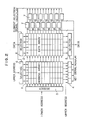
- Figs. 5 and 7 show a cache memory which comprises an address array 1 for storing addresses of a main storage, and a data array 2 for storing the contents of the addresses.
- the addresses and contents of the main storage are stored in corresponding blocks of the two arrays 1 and 2, respectively.
- Each of the blocks of the cache memory has one word capacity.
- a lower address of the given address is decoded in a decoder 3 to select a row which is called a "set" of the address array 1 as well as selecting a row (set) of the data array 2.
- a comparison circuit 4 compares in parallel an upper address of the given address with addresses stored in four blocks which are called "elements" of the selected set of the address array 1. If an address stored in any one of the elements coincides with the upper address, a selector 5 selects the contents of an element of the data array 2 corresponding to the element of the address array 1 storing the upper address, and reads out the contents of the selected element.
- the main storage is accessed. Then, the contents of an LRU element in the selected set of the address array 1 and the contents of an LRU element in the selected set of the data array 2 are replaced with the accessed address and contents of the main storage.
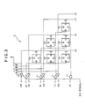
- the LRU circuit 17 shown in Fig. 2 is constituted as shown in Fig. 3. Each LRU circuit is provided for each of the sets of the cache memory.
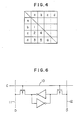
- the LRU circuit 17 comprises six R-S flip-flop circuits F/F 1 to 6. Output levels of the F/F 1 to 6 correspond to values at intersections 1 to 6 between rows "a" to "d” and columns "a" to "d” of the one half of a control table shown in Fig. 4.
- an accessed set of the cache memory transmits an enable signal EN to enable the LRU circuit 17 related to the accessed set. Further, a hit signal (ai, bi, ci or di) indicating an accessed one of elements of the accessed set is generated to set or reset the F/F circuits related to the rows and columns of the control table corresponding to the accessed element according to the algorithm of the LRU circuit. Then, an element specified with any one having a value of "1" among outputs "ao" to "do" is selected as an LRU element out of the element of the accessed set.
- selectors 6 select LRU elements among elements "a” to “d” of selected sets of both the address and data arrays according to the output signals "ao” to “do” from the LRU circuit 17, and the contents of the selected LRU elements are replaced with new data.
- This sort of LRU circuit can update LRU information at a speed equivalent to a cache memory accessing speed without using extra clock cycles.
- This circuit uses many elements to complicate wiring and hinder dense integration of the circuit.
- Fig. 5 shows another LRU circuit which comprises a memory cell array 8 and a control circuit 9.
- the number of rows corresponds to the number of sets of a cache memory, and each of the rows includes six memory cells necessary for storing LRU information related to four elements included in each of the sets of the cache memory.
- Fig. 6 shows the constitution of each memory cell of the LRU circuit of Fig. 5.
- a control line 10 is HIGH, the memory cell can be read or written through data lines 11 and 12.
- the control line 10 of a row of cells of the memory cell array 8 corresponding to the selected set of the cache memory is put in HIGH so that the LRU information may be read out of six cells contained in the above-mentioned row of the memory cell array 8.
- the read LRU information is inputted into the control circuit 9.
- the LRU information and a hit signal indicating an accessed element are inputted into the control circuit 9 to update the LRU information according to an LRU algorithm and rewrite it in the original six memory cells.
- control circuit 9 If a cache miss occurs, the control circuit 9 does not receive the hit signal so that the LRU information is not updated but rewritten as it is. Meanwhile, the control circuit 9 outputs an element selection signal (ao, bo, co or do) to selectors 7 to replace the contents of current LRU elements contained in accessed sets of the address and data arrays with new data.
- an element selection signal (ao, bo, co or do) to selectors 7 to replace the contents of current LRU elements contained in accessed sets of the address and data arrays with new data.
- This sort of LRU circuit can use the same memory cells as those used in a static RAM so that the memory cell array 8 may be integrated densely. This circuit, however, needs reading and writing operations in updating the LRU information to consume two memory cycles. Therefore, with this sort of LRU circuit, it is impossible to successively access the cache memory and a TLB (Translation Lookaside Buffer) each in one cycle so that a total operation speed may slow down.
- TLB Translation Lookaside Buffer
- An object of the present invention is to provide an LRU circuit which can update values in memory cells with no reading operation to realize a high-speed operation.
- the present invention provides an LRU circuit which comprises memory cells.
- Each of the memory cells has a control line enabling reading and writing operations, and two data lines used for the reading and writing operations.
- the memory cells are set in one of two statuses depending on the direction of a potential difference between the data lines, or held as they are if there is no potential difference between the data lines.
- the memory cells are arranged in a memory cell array.
- the number of columns (rows) of the memory cell array corresponds to the number of memory cells necessary to store binary LRU data required to execute an LRU algorithm on elements of each set, and the number of rows (columns) of the memory cell array corresponds to the number of sets.
- Memory cells in each row of the array are put in a reading and writing enabled state upon receiving a signal from one of the sets corresponding to the row in question of the array.
- the data lines of the memory cells in the same column are connected to each other in the direction of the column.
- the LRU circuit of the present invention further comprises an input control circuit which receives a hit signal indicating a used one of elements of a certain set and updates, according to the LRU algorithm, values in corresponding memory cells of the array through the column data lines, and an output control circuit for decoding values in the memory cells of specified one of the rows of the array to determine an LRU element.
- the LRU circuit of the present invention can update values in memory cells with no reading operation, thus realizing a high-speed operation. Further, the LRU circuit as a whole can be integrated densely.
- Fig. 7 is a view showing an LRU circuit according to an embodiment if the present invention.
- the LRU circuit is used for a four-way-set-associative type cache memory which is similar to those shown in Figs. 2 and 5.
- the LRU circuit 13 comprises a memory cell array 14, an input control circuit 15 and an output control circuit 16.
- the memory cell array 14 has rows whose number is the same as the number of sets contained in the cache memory, and each row includes six memory cells. According to this embodiment, values in six memory cells of each row correspond, from the left to the right, to values (1) to (6) in a control table shown in Fig. 8. Each of the memory cells has the same circuit constitution as that shown in Fig. 6.
- the input control circuit 15 when receiving a hit signal (ai, bi, ci or di) from a comparison circuit 4, updates LRU information stored in memory cells of a row whose control line is at HIGH due to an enable signal 171 transmitted from an accessed one of the sets in the cache memory.
- an external control signal may be provided to update or reset the LRU information.
- the input control circuit 15 outputs write signals to write 1 or 0 in the cells, and hold signals to hold values in the cells as they are.
- the input control circuit 15 provided write signals to write "1" in portions encircled with a continuous line shown in Fig. 8(B). These portions correspond to a leftmost memory cell of the above-mentioned certain row of the array 14. At the same time, the input control circuit 15 provides write signals to write "0" in portions encircled with a dotted line shown in the same figure. These portions correspond to the fourth and fifth memory cells from the left of the above-mentioned certain row of the array 14. To the other memory cells of the certain row, the input control circuit 15 provides hold signals.
- write masking signals may be provided to prevent values in the memory cells from changing.
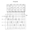
- Fig. 10 shows an example of the constitution of the input control circuit 15.
- the cells in respective columns of the memory cell array 14 have data lines D and D which are connected to column data lines Dl, D1 to D6, D6 .
- the column data lines are grounded through NMOS elements 17.
- Gates of the NMOS elements 17 which are connected to the column data lines D1 to D6 are connected with hit signals that correspond to the columns of the LRU control table, while gates of the NMOS elements 17 which are connected to the column data lines D1 to D6 are connected with hit signals that correspond to the rows of the LRU control table.
- control line C is HIGH, it is supposed to be “1” with the memory cell outputting a potential HIGH to the data line D, and it is supposed to be "0” with the memory cell outputting a potential LOW to the data line D.
- a table of Fig. 11 shows relations of hit signals for indicating accessed elements and outputs of the input control circuit 15. According to this table, values in memory cells of an enabled row are updated.
- the input control circuit 15 may comprise, instead of the NMOS elements, P-channel MOS transistors.
- the PMOS transistors are connected between a power source and the column data lines. Therefore, "1" and "0" are written in a manner opposite to the case of NMOS elements.
- the output control circuit 16 is a decoder which receives values in memory cells of an enabled row of the memory cell array 14 to determine an LRU element in a corresponding set of the cache memory, and sends an element selection signal to the selectors 7.
- Fig. 12 shows relations of values in respective memory cells and LRU elements determined according to the values.
- This kind of output control circuit 16 may easily be constituted by a logical circuit such as a PLA (Programmable Logic Array) circuit and a random logic circuit.
- values in memory cells in a row of the memory cell array corresponding to the accessed set of the cache memory are updated by the input control circuit 15 according to the LRU algorithm. If a cache miss occurs, values in memory cells in a row of the memory cell array corresponding to the accessed set of the cache memory are sent to the output control circuit 16 to determine an LRU element whose contents are replaced with the contents red out of the main storage.
- the LRU circuit of the present invention uses a memory cell array such as the one shown in Fig. 6 which can be integrated densely, together with a simple input control circuit such as the one shown in Fig. 10 to update values in cells of the memory cell array according to an LRU algorithm with no reading operation. Therefore, a high-speed operation and dense integration are realized.
- the LRU circuit of the present invention has been applied for the cache memory in this specification, the LRU circuit of the present invention is applicable not only for the cache memory but also for TLB, etc.
Landscapes
- Engineering & Computer Science (AREA)
- Theoretical Computer Science (AREA)
- Physics & Mathematics (AREA)
- General Engineering & Computer Science (AREA)
- General Physics & Mathematics (AREA)
- Memory System Of A Hierarchy Structure (AREA)
Applications Claiming Priority (2)
| Application Number | Priority Date | Filing Date | Title |
|---|---|---|---|
| JP63040687A JPH01216447A (ja) | 1988-02-25 | 1988-02-25 | Lru回路 |
| JP40687/88 | 1988-02-25 |
Publications (2)
| Publication Number | Publication Date |
|---|---|
| EP0330213A2 true EP0330213A2 (de) | 1989-08-30 |
| EP0330213A3 EP0330213A3 (de) | 1990-12-19 |
Family
ID=12587461
Family Applications (1)
| Application Number | Title | Priority Date | Filing Date |
|---|---|---|---|
| EP19890103219 Withdrawn EP0330213A3 (de) | 1988-02-25 | 1989-02-23 | LRU-Schaltung für Cache-Speicher |
Country Status (3)
| Country | Link |
|---|---|
| EP (1) | EP0330213A3 (de) |
| JP (1) | JPH01216447A (de) |
| KR (1) | KR910010136B1 (de) |
Family Cites Families (2)
| Publication number | Priority date | Publication date | Assignee | Title |
|---|---|---|---|---|
| JPS5771574A (en) * | 1980-10-21 | 1982-05-04 | Nec Corp | Siemconductor memory circuit |
| JPS62231350A (ja) * | 1986-03-31 | 1987-10-09 | Toshiba Corp | 論理回路 |
-
1988
- 1988-02-25 JP JP63040687A patent/JPH01216447A/ja active Granted
-
1989
- 1989-02-23 EP EP19890103219 patent/EP0330213A3/de not_active Withdrawn
- 1989-02-25 KR KR1019890002234A patent/KR910010136B1/ko not_active Expired
Also Published As
| Publication number | Publication date |
|---|---|
| JPH0550020B2 (de) | 1993-07-27 |
| JPH01216447A (ja) | 1989-08-30 |
| KR910010136B1 (ko) | 1991-12-17 |
| EP0330213A3 (de) | 1990-12-19 |
| KR890013566A (ko) | 1989-09-23 |
Similar Documents
| Publication | Publication Date | Title |
|---|---|---|
| US4683555A (en) | Serial accessed semiconductor memory with reconfigureable shift registers | |
| US5752260A (en) | High-speed, multiple-port, interleaved cache with arbitration of multiple access addresses | |
| US4831522A (en) | Circuit and method for page addressing read only memory | |
| US4648077A (en) | Video serial accessed memory with midline load | |
| US4636986A (en) | Separately addressable memory arrays in a multiple array semiconductor chip | |
| CA1224566A (en) | Content addressable memory cell | |
| US4667313A (en) | Serially accessed semiconductor memory with tapped shift register | |
| EP0355560A2 (de) | Bedingungsschreib-RAM | |
| EP0189576B1 (de) | Mehrfachvideospeichersystem mit Bildelementkartierung | |
| JPH04233825A (ja) | プログラマブル論理装置、この装置で使用する回路ブロック、及び前記装置への入力が論理機能で使用されるかどうかを決定する方法 | |
| US3644906A (en) | Hybrid associative memory | |
| EP0364110B1 (de) | Halbleiterspeichereinrichtung, die einen Speicher mit Seriengriff aufweist | |
| KR950000027B1 (ko) | 시리얼 입출력 반도체 메모리 | |
| US5165029A (en) | Cache memory with test function | |
| EP0564813A1 (de) | Bitleitungsschaltmatrix für elektronischen Rechnerspeicher | |
| KR100955251B1 (ko) | Sram 회로 및 이것을 이용한 버퍼 회로 | |
| US5121354A (en) | Random access memory with access on bit boundaries | |
| JPH0757469A (ja) | メモリ回路 | |
| EP0381940B1 (de) | Registerbankschaltung | |
| EP0330213A2 (de) | LRU-Schaltung für Cache-Speicher | |
| US5978245A (en) | Associative memory device having circuitry for storing a coincidence line output | |
| US5873126A (en) | Memory array based data reorganizer | |
| GB1278664A (en) | An associative memory | |
| US5166660A (en) | Random access compare array | |
| US5918075A (en) | Access network for addressing subwords in memory for both little and big endian byte order |
Legal Events
| Date | Code | Title | Description |
|---|---|---|---|
| PUAI | Public reference made under article 153(3) epc to a published international application that has entered the european phase |
Free format text: ORIGINAL CODE: 0009012 |
|
| 17P | Request for examination filed |
Effective date: 19890223 |
|
| AK | Designated contracting states |
Kind code of ref document: A2 Designated state(s): DE FR GB |
|
| RIN1 | Information on inventor provided before grant (corrected) |
Inventor name: SASAI, KIYOTAKA Inventor name: SASAKI, TOHRU |
|
| PUAL | Search report despatched |
Free format text: ORIGINAL CODE: 0009013 |
|
| AK | Designated contracting states |
Kind code of ref document: A3 Designated state(s): DE FR GB |
|
| 17Q | First examination report despatched |
Effective date: 19931005 |
|
| STAA | Information on the status of an ep patent application or granted ep patent |
Free format text: STATUS: THE APPLICATION IS DEEMED TO BE WITHDRAWN |
|
| 18D | Application deemed to be withdrawn |
Effective date: 19940216 |