EP0327475A1 - Structure de protection des sorties d'un circuit intégré de type MOS - Google Patents
Structure de protection des sorties d'un circuit intégré de type MOS Download PDFInfo
- Publication number
- EP0327475A1 EP0327475A1 EP89420027A EP89420027A EP0327475A1 EP 0327475 A1 EP0327475 A1 EP 0327475A1 EP 89420027 A EP89420027 A EP 89420027A EP 89420027 A EP89420027 A EP 89420027A EP 0327475 A1 EP0327475 A1 EP 0327475A1
- Authority
- EP
- European Patent Office
- Prior art keywords
- protection
- voltage
- protected
- drain
- mos
- Prior art date
- Legal status (The legal status is an assumption and is not a legal conclusion. Google has not performed a legal analysis and makes no representation as to the accuracy of the status listed.)
- Withdrawn
Links
- 230000004224 protection Effects 0.000 title claims abstract description 35
- 230000002457 bidirectional effect Effects 0.000 claims abstract description 19
- 230000015556 catabolic process Effects 0.000 claims abstract description 13
- 239000000758 substrate Substances 0.000 claims description 13
- 238000001465 metallisation Methods 0.000 claims description 8
- 230000001681 protective effect Effects 0.000 claims 1
- 230000001066 destructive effect Effects 0.000 description 4
- 238000010586 diagram Methods 0.000 description 3
- 238000005516 engineering process Methods 0.000 description 2
- 235000021183 entrée Nutrition 0.000 description 2
- 230000010287 polarization Effects 0.000 description 2
- 206010043268 Tension Diseases 0.000 description 1
- 238000004458 analytical method Methods 0.000 description 1
- 230000007423 decrease Effects 0.000 description 1
- 238000004519 manufacturing process Methods 0.000 description 1
- 238000000034 method Methods 0.000 description 1
- 230000003071 parasitic effect Effects 0.000 description 1
- 239000004065 semiconductor Substances 0.000 description 1
- 230000001960 triggered effect Effects 0.000 description 1
Images


Classifications
-
- H—ELECTRICITY
- H01—ELECTRIC ELEMENTS
- H01L—SEMICONDUCTOR DEVICES NOT COVERED BY CLASS H10
- H01L29/00—Semiconductor devices adapted for rectifying, amplifying, oscillating or switching, or capacitors or resistors with at least one potential-jump barrier or surface barrier, e.g. PN junction depletion layer or carrier concentration layer; Details of semiconductor bodies or of electrodes thereof ; Multistep manufacturing processes therefor
- H01L29/66—Types of semiconductor device ; Multistep manufacturing processes therefor
- H01L29/68—Types of semiconductor device ; Multistep manufacturing processes therefor controllable by only the electric current supplied, or only the electric potential applied, to an electrode which does not carry the current to be rectified, amplified or switched
- H01L29/76—Unipolar devices, e.g. field effect transistors
- H01L29/772—Field effect transistors
- H01L29/78—Field effect transistors with field effect produced by an insulated gate
-
- H—ELECTRICITY
- H01—ELECTRIC ELEMENTS
- H01L—SEMICONDUCTOR DEVICES NOT COVERED BY CLASS H10
- H01L27/00—Devices consisting of a plurality of semiconductor or other solid-state components formed in or on a common substrate
- H01L27/02—Devices consisting of a plurality of semiconductor or other solid-state components formed in or on a common substrate including semiconductor components specially adapted for rectifying, oscillating, amplifying or switching and having at least one potential-jump barrier or surface barrier; including integrated passive circuit elements with at least one potential-jump barrier or surface barrier
- H01L27/0203—Particular design considerations for integrated circuits
- H01L27/0248—Particular design considerations for integrated circuits for electrical or thermal protection, e.g. electrostatic discharge [ESD] protection
- H01L27/0251—Particular design considerations for integrated circuits for electrical or thermal protection, e.g. electrostatic discharge [ESD] protection for MOS devices
- H01L27/0255—Particular design considerations for integrated circuits for electrical or thermal protection, e.g. electrostatic discharge [ESD] protection for MOS devices using diodes as protective elements
Definitions
- An integrated circuit includes input pads and output pads. Overvoltages applied to these pads can destroy the circuit.
- An input pad is generally connected to at least one MOS transistor gate, and an output pad to at least one drain - or a source - of MOS transistor.
- the gate of a MOS transistor being a particularly fragile element, it constitutes the element mainly affected during the application of overvoltages. The effort on overvoltage protection therefore focused initially on the protection of the circuit's input gates.
- the protections of the input grids have made such progress that the drains / sources of output from the circuits are becoming the critical point. It is therefore essential to provide protection structures for drains / circuit output sources.
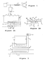
- FIG. 1 represents an example of a conventional input protection assembly of an MOS circuit.
- a conduction device bidirectional tion 1 is connected between an input pad 2, connected to the input gates 3 of the circuit to be protected, and a reference voltage 5, commonly ground.
- a resistor 4 is connected between the bidirectional conduction device 1 and the input gates 3 of the circuit.
- FIG. 2A shows a top view of an example of conventional bidirectional conduction device and Figure 2B shows a sectional view along AA of the device shown in Figure 2A.
- It is a device of type N+P ⁇ N+, comprising a first region 10 of type N+ connected to the input pad 2 by a contact 11, the part P ⁇ being constituted by the substrate 12 and another region 13 of type N+ being connected to the reference voltage by a contact 21.
- the first NP junction 14 formed of the region 10 of type N+ and of the part P ⁇ constituted by the substrate 12 connected to ground is in direct polarization and the overvoltage will be absorbed by the ground connection of the substrate.
- the first PN junction 14 is reverse biased. It goes in an avalanche for an overvoltage greater than a value V Z (approximately 20 volts) and the current begins to be evacuated by the ground connection of the substrate. Since the substrate is very resistive, its potential increases at the level of the second N+ 13 type region. As soon as the potential of the substrate exceeds 0.6 V, the second PN junction 15 formed of the part P ⁇ constituted by the substrate 12 and of region N de type 13 is in direct polarization. The overvoltage will then be absorbed by the avalanche of the structure P+N ⁇ P+.
- FIG. 3 represents an example of a conventional input protection assembly viewed from above on the wafer which supports the integrated circuit to be protected.
- a bidirectional conduction device 1 of the type shown in FIGS. 2A and 2B is connected on the one hand to an input pad 2 of the circuit by a contact 11 on the other hand to a metallization 20, located at the reference voltage, by a contact 21.
- the N+ type region 10 of this device which is connected to the stud comprises an extension 22 of considerable length before its width, this length extending in a direction which moves away from the device P +N ⁇ P+. This extension constitutes a resistor whose other end is connected by a metallization 23 to at least one input gate of the circuit (not shown in the figure).
- the value of the resistance must make it possible to drop the voltage which appears during the appearance of an overvoltage pulse on the pad 2, to a non-destructive value for the circuit.
- Each surface element between the extension N+ and the substrate P ⁇ constitutes an elementary Zener diode.
- the total interface between the resistor and the substrate corresponds to a distributed Zener diode.
- the voltage in the substrate during the pulse also high in the vicinity of the pad because of the fairly high value of the resistance of the part P ⁇ formed by the substrate 12 and the fairly large current which can pass between the region 10 and the P ⁇ part, decreases progressively when one moves away from the stud along the resistance and reaches a value close to 0 V at the end of the extension opposite to the stud.
- an object of the present invention is to provide a mode of protection of an MOS integrated circuit output terminal which does not harm the operation of the circuit.
- FIG. 4 represents a type of output protection structure of an MOS circuit which one might think of adopting on reading the documents of the prior art, namely a bidirectional conduction device without serial resistance between the pad and the device to be protected.
- a bidirectional conduction device 30 is connected between an output pad 31, connected to drains / output source 32 of the circuit to be protected, and a reference voltage, commonly ground.
- FIG. 5 represents on the same diagram, in the case where a pulse is applied to the pad 31 of the structure shown in FIG. 4, on the one hand, the voltage of the pulse dion, dotted line, which increases rapidly over time, on the other hand, the voltage at the drains / sources which increases simultaneously and stabilizes when the value of the voltage at the conduction V c of the MOS transistor is reached.
- the voltage V T is the breakdown voltage of the protection device. Current manufacturing technologies mean that the voltage V T is greater than the voltage V c if one does not want to resort to complex processes. Thus, during the pulse, the transistor will be put in conduction mode and will allow a destructive current to pass before the bidirectional conduction device is triggered.
- FIG. 6 represents a top view of an embodiment of an exit protection structure according to the present invention.
- a bidirectional conduction device similar to that shown in Figure 2, is connected between the pad 31 and a metallization 50 connected to the reference voltage.
- This bidirectional conduction device consists of a first region 51 of type N+, which is connected by a contact 52 to pad 31, of a part P enamel, which is the substrate 53, and of a second region 54 of type N+ connected by a contact 55 to the metallization 50 (ground).
- the N 51 type region 51 includes a short extension 56.
- This extension constitutes a resistor whose other end is connected by a metallization 57 to the drains / sources of the circuit to be protected (not shown in the figure).
- the time constants are such that, when an overvoltage is applied, the MOS transistor conducts first as soon as the voltage reaches the va their V c ; then the current increases, due to the voltage drop in the resistor constituted by the extension 56, the voltage on the region 51 of the N type type becomes greater than the breakdown voltage V T of the protection device.
- the value of the resistance of the extension 56 is chosen so that the product of this value by a current less than the maximum admissible current in the drains / sources of the transistors to be protected is slightly greater than the difference between the breakdown voltage V T of the device protection and the conduction voltage V c on the drains / sources of the transistors. In practice, with the usual technologies for doping the N+ regions, this resistance will have, when viewed from above, a surface corresponding to one to two squares, that is to say a value much lower than that of the extension 22 of FIG. 2 .
- the time constants of the circuit are such that the voltage V T is reached on the pad, before the voltage on the drain reaches the value VC.
- current will flow through the transistor if the pulse has not already been absorbed by the protection, but, due to the aforementioned choice of the value of resistor 56, this current in the drain will not be destructive.
- the resistor 56 has a different function from that of the resistor 22 of the known gate protection circuits. Indeed, in the case of gate protection circuits, it was sought to avoid any conduction of the gates. According to the invention, for the protection of drains or sources, it is only sought to limit the breakdown current, which makes it possible to choose resistors with non-zero but very low values which do not obstruct the proper normal operation of the output stages.
Applications Claiming Priority (2)
| Application Number | Priority Date | Filing Date | Title |
|---|---|---|---|
| FR8801551A FR2627028B1 (fr) | 1988-02-04 | 1988-02-04 | Structure de protection des sorties d'un circuit integre de type mos |
| FR8801551 | 1988-02-04 |
Publications (1)
| Publication Number | Publication Date |
|---|---|
| EP0327475A1 true EP0327475A1 (fr) | 1989-08-09 |
Family
ID=9363122
Family Applications (1)
| Application Number | Title | Priority Date | Filing Date |
|---|---|---|---|
| EP89420027A Withdrawn EP0327475A1 (fr) | 1988-02-04 | 1989-02-01 | Structure de protection des sorties d'un circuit intégré de type MOS |
Country Status (4)
| Country | Link |
|---|---|
| EP (1) | EP0327475A1 (ko) |
| JP (1) | JPH025571A (ko) |
| KR (1) | KR890013795A (ko) |
| FR (1) | FR2627028B1 (ko) |
Cited By (2)
| Publication number | Priority date | Publication date | Assignee | Title |
|---|---|---|---|---|
| EP0624906A1 (en) * | 1993-05-13 | 1994-11-17 | Consorzio per la Ricerca sulla Microelettronica nel Mezzogiorno - CoRiMMe | Integrated structure circuit for the protection of power devices against overvoltages |
| US5777367A (en) * | 1993-09-30 | 1998-07-07 | Consorzio Per La Ricerca Sulla Microelettronica Nel Mezzogiorno | Integrated structure active clamp for the protection of power devices against overvoltages |
Family Cites Families (2)
| Publication number | Priority date | Publication date | Assignee | Title |
|---|---|---|---|---|
| JPS6038858A (ja) * | 1983-08-12 | 1985-02-28 | Hitachi Ltd | 半導体集積回路装置 |
| JPH0665224B2 (ja) * | 1984-04-20 | 1994-08-22 | 日立マイクロコンピュ−タエンジニアリング株式会社 | 半導体集積回路装置 |
-
1988
- 1988-02-04 FR FR8801551A patent/FR2627028B1/fr not_active Expired - Lifetime
-
1989
- 1989-02-01 EP EP89420027A patent/EP0327475A1/fr not_active Withdrawn
- 1989-02-01 KR KR1019890001162A patent/KR890013795A/ko not_active Application Discontinuation
- 1989-02-03 JP JP1025582A patent/JPH025571A/ja active Pending
Non-Patent Citations (1)
| Title |
|---|
| PATENT ABSTRACTS OF JAPAN * |
Cited By (3)
| Publication number | Priority date | Publication date | Assignee | Title |
|---|---|---|---|---|
| EP0624906A1 (en) * | 1993-05-13 | 1994-11-17 | Consorzio per la Ricerca sulla Microelettronica nel Mezzogiorno - CoRiMMe | Integrated structure circuit for the protection of power devices against overvoltages |
| US5652455A (en) * | 1993-05-13 | 1997-07-29 | Consorzio Per La Ricerca Sulla Microelettronica Nel Mezzogiorno | Integrated structure circuit for the protection of power devices against overvoltage |
| US5777367A (en) * | 1993-09-30 | 1998-07-07 | Consorzio Per La Ricerca Sulla Microelettronica Nel Mezzogiorno | Integrated structure active clamp for the protection of power devices against overvoltages |
Also Published As
| Publication number | Publication date |
|---|---|
| JPH025571A (ja) | 1990-01-10 |
| FR2627028B1 (fr) | 1990-07-20 |
| KR890013795A (ko) | 1989-09-26 |
| FR2627028A1 (fr) | 1989-08-11 |
Similar Documents
| Publication | Publication Date | Title |
|---|---|---|
| EP0568421B1 (fr) | Dispositif de protection d'un circuit intégré contre les décharges électrostatiques | |
| EP0316211B1 (fr) | Circuit intégré protégé contre des décharges électrostatiques, avec seuil de protection variable | |
| EP0543742B1 (fr) | Diode de protection monolithique basse tension à faible capacité | |
| FR2631167A1 (fr) | Circuit integre comportant une protection contre les decharges electrostatiques | |
| FR2499315A1 (fr) | Dispositif semiconducteur de protection utilisant des diodes zener dos a dos | |
| FR2533369A1 (fr) | Circuit de protection pour dispositifs a circuit integre et structure de semi-conducteur pour proteger un circuit integre | |
| EP0515282B1 (fr) | Structure de protection dans un circuit CMOS contre le verrouillage | |
| FR2812972A1 (fr) | Dispositif a semiconducteur consistant en un thyristor pour la protection contre les decharges electrostatiques | |
| FR2685817A1 (fr) | Protection generale d'un circuit integre contre les surcharges permanentes et decharges electrostatiques. | |
| FR2494501A1 (fr) | Protection d'entree pour circuit integre de type mos a basse tension d'alimentation et a haute densite d'integration | |
| EP0664564B1 (fr) | Circuit intégré incorporant une protection contre les décharges électrostatistiques | |
| FR2694851A1 (fr) | Circuit de tirage vers un état déterminé d'une entrée de circuit intégré. | |
| EP0326777B1 (fr) | Structure de protection d'un accès à un circuit intégré | |
| FR2748854A1 (fr) | Structure de protection contre une decharge electrostatique pour circuit integre cmos | |
| FR2613131A1 (fr) | Circuit integre protege contre des surtensions | |
| FR2507819A1 (fr) | Dispositif de protection contre les surcharges pour circuit integre et circuit integre de protection contre les surcharges | |
| FR2582861A1 (fr) | Dispositif de protection contre des decharges electrostatiques, notamment pour des circuits integres bipolaires | |
| EP0518790B1 (fr) | Composant de protection bidirectionnel | |
| EP1638146A2 (fr) | Circuit électronique à double alimentation et à moyens de protection contre les claquages, et moyens de protection correspondants | |
| EP0327475A1 (fr) | Structure de protection des sorties d'un circuit intégré de type MOS | |
| FR2719158A1 (fr) | Circuit d'entrée pour protéger un circuit intégré monolithe. | |
| FR2904473A1 (fr) | Dispositif de protection d'un circuit integre contre les decharges electrostatiques | |
| FR2741756A1 (fr) | Circuit de protection contre les surtensions | |
| FR3106941A1 (fr) | Protection contre des surtensions | |
| EP0886316A1 (fr) | Protection du caisson logique d'un composant incluant un transistor MOS de puissance intégré |
Legal Events
| Date | Code | Title | Description |
|---|---|---|---|
| PUAI | Public reference made under article 153(3) epc to a published international application that has entered the european phase |
Free format text: ORIGINAL CODE: 0009012 |
|
| AK | Designated contracting states |
Kind code of ref document: A1 Designated state(s): DE FR GB IT NL |
|
| STAA | Information on the status of an ep patent application or granted ep patent |
Free format text: STATUS: THE APPLICATION IS DEEMED TO BE WITHDRAWN |
|
| 18D | Application deemed to be withdrawn |
Effective date: 19900210 |