EP0327420A1 - Vorrichtung und Verfahren zur Messung eines kurzen Lichtimpulses oder eines kurzen elektrischen Impulses - Google Patents
Vorrichtung und Verfahren zur Messung eines kurzen Lichtimpulses oder eines kurzen elektrischen Impulses Download PDFInfo
- Publication number
- EP0327420A1 EP0327420A1 EP89400158A EP89400158A EP0327420A1 EP 0327420 A1 EP0327420 A1 EP 0327420A1 EP 89400158 A EP89400158 A EP 89400158A EP 89400158 A EP89400158 A EP 89400158A EP 0327420 A1 EP0327420 A1 EP 0327420A1
- Authority
- EP
- European Patent Office
- Prior art keywords
- pulse
- photoconductors
- measuring
- photoconductor
- line
- Prior art date
- Legal status (The legal status is an assumption and is not a legal conclusion. Google has not performed a legal analysis and makes no representation as to the accuracy of the status listed.)
- Granted
Links
- 238000000034 method Methods 0.000 title claims description 15
- 230000005855 radiation Effects 0.000 claims abstract description 33
- 239000000969 carrier Substances 0.000 claims abstract description 21
- 238000005311 autocorrelation function Methods 0.000 claims abstract description 14
- 238000004458 analytical method Methods 0.000 claims abstract description 8
- 239000003989 dielectric material Substances 0.000 claims abstract description 4
- 238000005259 measurement Methods 0.000 claims description 24
- 239000000758 substrate Substances 0.000 claims description 23
- 238000005070 sampling Methods 0.000 claims description 10
- 239000004065 semiconductor Substances 0.000 claims description 8
- 230000002123 temporal effect Effects 0.000 claims description 7
- MARUHZGHZWCEQU-UHFFFAOYSA-N 5-phenyl-2h-tetrazole Chemical compound C1=CC=CC=C1C1=NNN=N1 MARUHZGHZWCEQU-UHFFFAOYSA-N 0.000 claims description 6
- 238000000429 assembly Methods 0.000 claims description 4
- 230000000712 assembly Effects 0.000 claims description 4
- 230000003111 delayed effect Effects 0.000 claims description 4
- GPXJNWSHGFTCBW-UHFFFAOYSA-N Indium phosphide Chemical compound [In]#P GPXJNWSHGFTCBW-UHFFFAOYSA-N 0.000 claims description 2
- 238000009532 heart rate measurement Methods 0.000 claims description 2
- GYHNNYVSQQEPJS-UHFFFAOYSA-N Gallium Chemical compound [Ga] GYHNNYVSQQEPJS-UHFFFAOYSA-N 0.000 claims 1
- 229910052733 gallium Inorganic materials 0.000 claims 1
- 238000010586 diagram Methods 0.000 description 11
- 230000003252 repetitive effect Effects 0.000 description 7
- 238000012731 temporal analysis Methods 0.000 description 6
- 239000010453 quartz Substances 0.000 description 5
- 230000035945 sensitivity Effects 0.000 description 5
- VYPSYNLAJGMNEJ-UHFFFAOYSA-N silicon dioxide Inorganic materials O=[Si]=O VYPSYNLAJGMNEJ-UHFFFAOYSA-N 0.000 description 5
- 238000000151 deposition Methods 0.000 description 3
- PCHJSUWPFVWCPO-UHFFFAOYSA-N gold Chemical compound [Au] PCHJSUWPFVWCPO-UHFFFAOYSA-N 0.000 description 3
- 229910052737 gold Inorganic materials 0.000 description 3
- 239000010931 gold Substances 0.000 description 3
- 230000001902 propagating effect Effects 0.000 description 3
- VYZAMTAEIAYCRO-UHFFFAOYSA-N Chromium Chemical compound [Cr] VYZAMTAEIAYCRO-UHFFFAOYSA-N 0.000 description 2
- 229910052782 aluminium Inorganic materials 0.000 description 2
- XAGFODPZIPBFFR-UHFFFAOYSA-N aluminium Chemical compound [Al] XAGFODPZIPBFFR-UHFFFAOYSA-N 0.000 description 2
- 229910052804 chromium Inorganic materials 0.000 description 2
- 239000011651 chromium Substances 0.000 description 2
- 230000008021 deposition Effects 0.000 description 2
- 230000005670 electromagnetic radiation Effects 0.000 description 2
- 230000005865 ionizing radiation Effects 0.000 description 2
- 239000000463 material Substances 0.000 description 2
- 230000002441 reversible effect Effects 0.000 description 2
- JBRZTFJDHDCESZ-UHFFFAOYSA-N AsGa Chemical compound [As]#[Ga] JBRZTFJDHDCESZ-UHFFFAOYSA-N 0.000 description 1
- 229910001218 Gallium arsenide Inorganic materials 0.000 description 1
- 230000005668 Josephson effect Effects 0.000 description 1
- BQCADISMDOOEFD-UHFFFAOYSA-N Silver Chemical compound [Ag] BQCADISMDOOEFD-UHFFFAOYSA-N 0.000 description 1
- 230000003321 amplification Effects 0.000 description 1
- 230000015556 catabolic process Effects 0.000 description 1
- 238000005229 chemical vapour deposition Methods 0.000 description 1
- 230000001427 coherent effect Effects 0.000 description 1
- 238000007796 conventional method Methods 0.000 description 1
- 239000013078 crystal Substances 0.000 description 1
- 238000001514 detection method Methods 0.000 description 1
- 230000005684 electric field Effects 0.000 description 1
- 238000005516 engineering process Methods 0.000 description 1
- 238000005286 illumination Methods 0.000 description 1
- 230000010354 integration Effects 0.000 description 1
- 239000004922 lacquer Substances 0.000 description 1
- 238000001465 metallisation Methods 0.000 description 1
- 238000003199 nucleic acid amplification method Methods 0.000 description 1
- 230000003287 optical effect Effects 0.000 description 1
- 125000002524 organometallic group Chemical group 0.000 description 1
- 230000003071 parasitic effect Effects 0.000 description 1
- 230000010287 polarization Effects 0.000 description 1
- 239000011347 resin Substances 0.000 description 1
- 229920005989 resin Polymers 0.000 description 1
- 230000000630 rising effect Effects 0.000 description 1
- 229910052709 silver Inorganic materials 0.000 description 1
- 239000004332 silver Substances 0.000 description 1
- 238000004544 sputter deposition Methods 0.000 description 1
- 239000004575 stone Substances 0.000 description 1
- 238000012546 transfer Methods 0.000 description 1
- 238000012800 visualization Methods 0.000 description 1
Images


Classifications
-
- G—PHYSICS
- G01—MEASURING; TESTING
- G01R—MEASURING ELECTRIC VARIABLES; MEASURING MAGNETIC VARIABLES
- G01R29/00—Arrangements for measuring or indicating electric quantities not covered by groups G01R19/00 - G01R27/00
- G01R29/02—Measuring characteristics of individual pulses, e.g. deviation from pulse flatness, rise time or duration
Definitions
- the subject of the invention is a device and a method for measuring a brief radiation pulse or a brief electrical pulse which makes it possible, from a single pulse, to know either its auto-correlation function or its time form. .
- pulses By short pulses is meant pulses whose duration can range from 1 to 1000 picoseconds.
- this pulse is conventionally sampled by means of a sampling oscilloscope which makes it possible to take part of the information at each pulse and thus to construct by part the pulse shape.
- a Josephson effect analysis can also be performed. This sampling technique can only be applied to repetitive pulses.
- a streak camera in which the visualization of the phenomenon on a memory tube linked to an electronic deflection has a temporal revolution close to the picosecond for photonic pulses (X-ray, visible ultraviolet or infrared).
- photonic pulses X-ray, visible ultraviolet or infrared
- the different photoconductors associated with each delay line in fact only allow time measurements very close to each other and only allow to know the inclination of the incident beam relative to its axis of propagation which is supposed to be perpendicular to the plane of the photoconductors. detectors.
- the different delay lines have different lengths in order to obtain different points of the autocorrelation function of a pulse.
- the photoconductive elements and the lines of propagation of the electrical signals are produced in surface technology (tape on substrate).
- This has the drawback of greatly limiting the usable bias voltages, failing which the ionization of the air between the electrodes in the vicinity of the photoconductive elements introduces a parasitic current which can introduce untimely breakdowns.
- This limitation introduces a significant loss of sensitivity which explains the necessity of operation with repetitive pulses.
- This device therefore makes it possible to carry out, by sampling, the analysis of the electrical pulse by optically introducing the delay necessary for the sampling function.
- the object of the present invention is to remedy these problems. It relates to a device for measuring a single short pulse characterized in that it comprises at least one measuring assembly capable of carrying out p measurement points of a pulse of duration ⁇ , comprising a conductive line to which is connected by one of their electrodes, a set of photoconductors, the line and the photoconductors being placed between two dielectrics and characterized in that the line length separating the photoconductors in pairs is equal to the product of the propagation speed on this line by the ratio ⁇ / p, the photoconductors being chosen so that the lifetime of the majority carriers which constitute them is less than or equal to 10% of the duration of the pulse to be analyzed.
- the device thus makes it possible to obtain a temporal analysis or the autocorrelation function, either of a radiation pulse or an electrical pulse.
- the subject of the invention is also a device for measuring a pulse comprising a plurality of measuring assemblies for which the lifetime of the majority carriers of the photoconductors is different from one assembly to another so as to obtain an identical sensitivity. for different pulse durations.
- the subject of the invention is also a device for measuring a short pulse in which each measuring assembly comprises p + 1 photoconducers whose lifetime ⁇ of majority carriers is less than or equal to 10% of 8, so as to have p measuring points for a pulse of duration ⁇ .
- the measuring device comprises a first substrate comprising a first metallized face and a second face opposite the first on which are arranged conductive tracks and a conductive line substantially perpendicular to the tracks and spaced from the latter. It also includes a second substrate placed on the tracks and the conductive line, this second substrate comprising orifices of length greater than the space which resides between the conductive line and the tracks and being covered with a metallized layer.
- the photoconductors consist of blocks comprising a substrate on which a semiconductor layer is deposited then a first and a second contact placed on the semiconductor layer at each of the ends of the block, each block having dimensions such that it can be housed in a orifice of the second substrate, one contact being placed on the conductive line while the other is placed on a track.
- the photoconductors are produced from a semiconductor layer consisting of cadmium telluride or gallium arsenide or indium phosphide.
- the invention also relates to a method for measuring a pulse for which the device of the invention is used, and in which the conductive line is closed at its two ends by its characteristic impedance; in which a short pulse of radiation to be analyzed is sent, illuminating all the photoconductors and, in synchronism with this pulse, a shorter radiation pulse of duration substantially equal to or less than the lifetime of the majority carriers of the photoconductors on the first photoconductor, this photoconductor being polarized by a predetermined direct voltage. A set of charges corresponding to a sampling of the radiation pulse to be analyzed is obtained, each charge being recovered on an output electrode of each photoconductor except the first.
- the temporal form of the pulse to be analyzed is obtained with a temporal resolution which is equal to the lifetime of the carriers present in the photoconductors.
- the subject of the invention is also a method for measuring a short pulse for which a device according to the invention is used in which the conductive line to which the photoconducers are connected is closed on its characteristic impedance at one end only and in which a short electrical pulse to be analyzed is sent to the other end, a shorter radiation pulse being sent to these photoconductors in synchronism with the electric pulse, the duration of the radiation pulse being substantially equal to or less than the duration of life of the majority of photoconductor carriers, a set of charges corresponding to a sampling of the electrical pulse to be analyzed being obtained, each charge being recovered on an output electrode of each photoconductor.
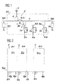
- the device for measuring a short pulse is illustrated in FIG. 1 by its electrical diagram.
- This measurement device comprises a conducting line L closed at its two ends 101 and 102 by its characteristic impedance Z0.
- a first photoconductor A is connected on the one hand to this line L and on the other hand to a bias voltage V.
- p photoconductors B1-Bp are connected on the one hand to this line L and on the other hand to integrating amplifiers I1, I2, ..., Ip, the photoconductor B1 being connected to an amplifier integrator I1, B2 to I2 and Bp to Ip.
- the device also includes p outputs Q1-Qp, each output corresponding to an output of an integrating amplifier. The distance x between each photoconductor is chosen equal to the product v.
- the distance between two photoconductors is therefore chosen so that it introduces a delay equal to the desired time interval between two successive points of the time analysis.
- the device according to the invention can comprise an assembly such as that shown in this FIG. 1 and which bears the reference Di, it can also comprise, according to an alternative embodiment, a plurality of assemblies Di, i ranging from 1 to n as is shown in FIG. 2. These assemblies are produced on the same support SP.
- the lifetime of the majority carriers of the photoconductors of each measurement set Di will be different from one set to another, for example a lifetime ⁇ 1 will be chosen for the set D1, ⁇ 2> ⁇ 1 for the set D2 and ⁇ n for the set Dn.
- An identical sensitivity is thus obtained for different pulse durations.
- Each set has a number of photoconductors equal to p + 1. If we choose a number p equal to 10, the first set will give 10 measurement points for a 100 ps pulse while the second set will give 5 measurement points for this same pulse, this second set will instead give 10 measurement points for a 200 ps pulse.
- each measurement set does not necessarily have to have the same number of photoconductors.
- FIG. 3A represents the electrical diagram of a device according to the invention corresponding to the assembly D1 of FIG. 2.
- FIG. 3B represents the electrical diagram of a device according to the invention corresponding to the assembly D2 of this same FIG. 2.
- the set of photoconductors A, B1, B2, Bp have a lifetime equal to ⁇ 1 while in the FIG. 3B these photoconductors A, B1, Bp have majority carriers which have a lifetime equal to ⁇ 2.
- the electric path traveled by the current on the line of the assembly D1 between two photoconductors B1, B2 or B2, B3 ..., is equal to x1, this path is equal to the length of the line between two adjacent photoconductors and is chosen equal to the product of the speed of propagation on the line by the desired time interval ⁇ A / p between two points of the temporal analysis of a pulse of duration ⁇ A.
- x2 v. ( ⁇ B / p) to perform a temporal analysis of a pulse of duration ⁇ B.
- the photoconductors are chosen so as to have a high resistivity in the absence of radiation (> 108lcm) so that the device has good dynamics.
- the charges accumulated by the outputs Qi in the absence of illumination are directly linked to the resistance of the photoconductive elements of type A and B considered to be polarized in series.
- the sensitivity being proportional to the bias voltage, it is preferable to use a high value for this bias voltage, a high resistivity being necessary to ensure good resistance in the electric field.
- FIG. 4 the structure of the device according to the invention is shown according to an embodiment according to the invention in which the line and the photoconductors are on the same support taken between two dielectrics, one of the dielectric which can be a gas or a vacuum.
- This structure comprises a first substrate 10 which has a first face 11 fully metallized, constituting a ground plane and which has a second face 12, partially metallized.
- the metallized parts constitute, on the one hand, a set of tracks 13 to which the integrating amplifiers I1-Ip are connected to form the outputs Q1, Q2, Qp of each set as shown in FIGS.
- these metallized zones also include a track 14 perpendicular to the tracks 13, this track 14 constitutes the conductive line L as can be seen in FIGS. 3A and 3B.
- the conductive track 14 is at a predetermined distance from the ends of the tracks 13 so that there is no contact between them.
- a second substrate 20 which comprises a set of orifices of length greater than the space which resides between the conductive track 14 and the tracks 13, so that an area 140 of the track 14 is not covered by the substrate 20 and so that a zone 130 of a given track 13, facing the track 14, is also not covered by this substrate 20.
- the face of the substrate 20 opposite the metallized face 12 of the substrate 10 is also covered with a metallization 220.
- Each photoconductor is produced so as to have the shape of a block 30 of dimensions such that it can be housed inside an orifice 21 of the support 20.
- the block 30 is constituted by a substrate 31 on which is deposited a layer of semiconductor material 32.
- a contact 33 and a contact 34 are made above this semiconductor material and at each of the ends of the block.
- the contact 33 is placed on the area 140 of the conductive track 14 and the contact 34 is placed on the area 130 of a track 13.
- each detection unit that is to say each photoconductor, is in the form of a quartz block of 125 ⁇ m thick, 200 ⁇ m wide, and 800 m long, on which a deposit of cadmium telluride 10 ⁇ m thick was made, the zones 140 and 130 having a width of 100 ⁇ m to allow contact with the paving stone.
- Each of these blocks is attached or glued with silver lacquer on tracks 14 and 13. These tracks are produced by depositing an aluminum layer on the quartz substrate 10 which has a thickness of 125 ⁇ m, the second substrate 20 is also made of quartz with the same thickness and is glued above the tracks using an insulating resin.
- Each photoconductor is obtained from a quartz substrate of 20 mm ⁇ 20 mm and a thickness equal to 125 ⁇ m onto which 12 ⁇ m cadmium telluride is deposited by a conventional technique known as OMCVD (Organometallic chemical vapor deposition).
- Conductive lines 14 are made of aluminum and are 5 ⁇ m thick and have a length of a few tens of millimeters.
- the plate is cut using a conventional saw suitable for these techniques.
- the quartz paver is positioned at the location of the contacts using a suction pump for example.
- the entire substrate 20 which includes the orifices is covered.
- FIG. 5 a particular example of a circuit for measuring the life of the majority carriers of a photoconductor intended to equip the measuring device has been shown diagrammatically.
- the principle of the measurement is as follows: as shown in this figure, an elementary pattern of the measuring device is used, this pattern therefore comprising a photoconductor A and a photoconductor B1 connected to the line L, the line being closed on its impedance characteristic Z0.
- the pattern is illuminated by very short laser pulses La .
- the answer to output Q1 is then directly a function of the lifespan of the carriers.
- the invention also relates to a method for measuring a short pulse for which the device which has just been described is used.
- the device makes it possible to measure points of the autocorrelation function of a single brief pulse either of radiation (electromagnetic or ionizing) or electric. It also makes it possible, from a single pulse to be analyzed, to obtain the time profile of this pulse whether it comes from electromagnetic or ionizing radiation or from an electric pulse.
- This device provides measurements without time linearity problem.
- the element Di has photoconductors whose majority carriers have a lifetime less than or equal to 10% of the duration of the pulse to be analyzed, and will provide p points of the autocorrelation function of this pulse.
- the reference photoconductors A are each polarized by a direct voltage.
- the lines L are closed at their ends on their characteristic impedance Z0.
- the distance x between each photoconductor is the electrical path traveled by the signal S (t), that is to say the length of the conductive line L between each photoconductor, this length has been determined from the duration of the pulse. and the number of measurement points, that is to say from the time intervals desired for the analysis.
- the delay x / v is therefore equal to ⁇ / p.
- the speed v of spread on the line is known.
- a charge Q1, for the photoconductor B1, (Qi for Bi) which is the result after amplification and integration of the convolution product is collected at the output of each photoconductor. Each charge collected corresponds to the measurement of a point in the autocorrelation function.
- the invention also relates to a method for performing a temporal analysis of a single brief pulse from the device according to the invention.
- the photoconductors A are polarized by a DC voltage.
- the lines L are closed on their characteristic impedance Z0 at the two ends.
- We send a short pulse of radiation E (t) which illuminates all the photoconductors and we send in synchronism with the rising edge of the radiation pulse another radiation pulse r (t) of extremely short duration compared to the range of duration that the first impulse can have.
- FIG. 6 shows the pulse E (t) and the propagation of the electric image on line L of the pulse r (t) as a function of time.
- the duration of the second pulse is less than or equal to the lifetime of the photoconductor carriers of the subassembly considered.
- This pulse r (t) lights up the polarized photoconductors A.
- the photoconductors B1-Bp are sequentially polarized by the signal propagating on the line, produced by this very short pulse. Is collected at the outputs of an element Di of the device, a set of charges corresponding to a temporal sampling of the radiation pulse to be analyzed E (t).
- the shortest pulse provides, like a strobe, an exact image in p points of the profile of the pulse to be analyzed.
- the invention also relates to a method for to perform a temporal analysis of a brief electrical pulse from the device according to the invention.
- the photoconductors A are not polarized by a DC voltage (they can be deleted) and the lines are closed on their characteristic impedance only at one end as can be seen in the diagram in Figure 7.
- a very short pulse of radiation r (t) illuminating the photoconductors B is sent.
- the duration of this very brief radiation pulse may correspond, for example, to the lifetime of the photoconductors of the subassembly considered
- This radiation pulse induces a time window for analyzing the pulse to be analyzed by making the elements B1-Bp conductive.
- the state of polarization of the various elements B1-Bp is a function of the voltage seen at its terminals which is directly linked to the shape of the pulse EL (t) propagating in the line L.
- the shortest pulse (of radiation) r (t) creates, like a stroboscope, an exact image, in p points of the profile of the electrical pulse to be analyzed EL (t).
Landscapes
- Physics & Mathematics (AREA)
- General Physics & Mathematics (AREA)
- Photometry And Measurement Of Optical Pulse Characteristics (AREA)
Applications Claiming Priority (2)
| Application Number | Priority Date | Filing Date | Title |
|---|---|---|---|
| FR8800694A FR2626376B1 (fr) | 1988-01-22 | 1988-01-22 | Dispositif et procede de mesure d'une impulsion breve de rayonnement ou d'une impulsion breve electrique |
| FR8800694 | 1988-01-22 |
Publications (2)
| Publication Number | Publication Date |
|---|---|
| EP0327420A1 true EP0327420A1 (de) | 1989-08-09 |
| EP0327420B1 EP0327420B1 (de) | 1993-04-21 |
Family
ID=9362522
Family Applications (1)
| Application Number | Title | Priority Date | Filing Date |
|---|---|---|---|
| EP89400158A Expired - Lifetime EP0327420B1 (de) | 1988-01-22 | 1989-01-19 | Vorrichtung und Verfahren zur Messung eines kurzen Lichtimpulses oder eines kurzen elektrischen Impulses |
Country Status (6)
| Country | Link |
|---|---|
| US (1) | US4933634A (de) |
| EP (1) | EP0327420B1 (de) |
| JP (1) | JPH02110384A (de) |
| CA (1) | CA1323503C (de) |
| DE (1) | DE68906039T2 (de) |
| FR (1) | FR2626376B1 (de) |
Cited By (4)
| Publication number | Priority date | Publication date | Assignee | Title |
|---|---|---|---|---|
| EP0559274A2 (de) * | 1992-03-03 | 1993-09-08 | Koninklijke Philips Electronics N.V. | Tastkopfgerät und Verfahren zum Messen von Hochfrequenzsignalen |
| FR2742866A1 (fr) * | 1995-12-22 | 1997-06-27 | Commissariat Energie Atomique | Procede et dispositif de caracterisation d'un milieu ionise mettant en oeuvre une source de rayonnement electromagnetique a duree ultracourte |
| FR2742867A1 (fr) * | 1995-12-22 | 1997-06-27 | Commissariat Energie Atomique | Procede et dispositif interferometrique de caracterisation d'un milieu |
| FR2766576A1 (fr) * | 1997-07-23 | 1999-01-29 | Commissariat Energie Atomique | Dispositif d'analyse d'impulsion unique a pas variable |
Families Citing this family (22)
| Publication number | Priority date | Publication date | Assignee | Title |
|---|---|---|---|---|
| US5142224A (en) * | 1988-12-13 | 1992-08-25 | Comsat | Non-destructive semiconductor wafer probing system using laser pulses to generate and detect millimeter wave signals |
| US5216359A (en) * | 1991-01-18 | 1993-06-01 | University Of North Carolina | Electro-optical method and apparatus for testing integrated circuits |
| US5159262A (en) * | 1991-07-09 | 1992-10-27 | Cascade Microtech, Inc. | Method for measuring the electrical and optical performance of on-wafer microwave devices |
| JP2726587B2 (ja) * | 1991-11-29 | 1998-03-11 | 株式会社東芝 | 電子ビーム照射装置および電気信号検出装置 |
| US5926950A (en) * | 1995-12-28 | 1999-07-27 | Fuji Machine Mfg. Co., Ltd. | Electronic component transferring device and method, and electronic component mounting system and method |
| US6168009B1 (en) | 1995-12-28 | 2001-01-02 | Fuji Machine Mfg. Co. Ltd. | Apparatus for positioning electronic component holder head and apparatus for transferring electronic component |
| US7088925B1 (en) * | 1999-06-28 | 2006-08-08 | Siemens Aktiengesellschaft | Device for detecting polarization mode dispersion |
| US6445202B1 (en) | 1999-06-30 | 2002-09-03 | Cascade Microtech, Inc. | Probe station thermal chuck with shielding for capacitive current |
| US6512385B1 (en) | 1999-07-26 | 2003-01-28 | Paul Pfaff | Method for testing a device under test including the interference of two beams |
| US6914423B2 (en) | 2000-09-05 | 2005-07-05 | Cascade Microtech, Inc. | Probe station |
| US6965226B2 (en) | 2000-09-05 | 2005-11-15 | Cascade Microtech, Inc. | Chuck for holding a device under test |
| US7206078B2 (en) | 2002-05-03 | 2007-04-17 | Attofemto, Inc. | Non-destructive testing system using a laser beam |
| US8462350B2 (en) | 2001-12-06 | 2013-06-11 | Attofemto, Inc. | Optically enhanced holographic interferometric testing methods for the development and evaluation of semiconductor devices, materials, wafers, and for monitoring all phases of development and manufacture |
| US7733499B2 (en) * | 2001-12-06 | 2010-06-08 | Attofemto, Inc. | Method for optically testing semiconductor devices |
| US9952161B2 (en) | 2001-12-06 | 2018-04-24 | Attofemto, Inc. | Methods for obtaining and analyzing digital interferometric data for computer testing and developing semiconductor and anisotropic devices and materials |
| US7400411B2 (en) | 2001-12-06 | 2008-07-15 | Attofemto, Inc. | Method for optically testing semiconductor devices |
| US7492172B2 (en) | 2003-05-23 | 2009-02-17 | Cascade Microtech, Inc. | Chuck for holding a device under test |
| US7250626B2 (en) | 2003-10-22 | 2007-07-31 | Cascade Microtech, Inc. | Probe testing structure |
| US7187188B2 (en) | 2003-12-24 | 2007-03-06 | Cascade Microtech, Inc. | Chuck with integrated wafer support |
| US7535247B2 (en) | 2005-01-31 | 2009-05-19 | Cascade Microtech, Inc. | Interface for testing semiconductors |
| US7656172B2 (en) | 2005-01-31 | 2010-02-02 | Cascade Microtech, Inc. | System for testing semiconductors |
| US8319503B2 (en) | 2008-11-24 | 2012-11-27 | Cascade Microtech, Inc. | Test apparatus for measuring a characteristic of a device under test |
Citations (1)
| Publication number | Priority date | Publication date | Assignee | Title |
|---|---|---|---|---|
| US4482863A (en) * | 1981-08-14 | 1984-11-13 | At&T Bell Laboratories | Apparatus and method for measuring electronic response of high speed devices and materials |
Family Cites Families (4)
| Publication number | Priority date | Publication date | Assignee | Title |
|---|---|---|---|---|
| US3278846A (en) * | 1962-05-03 | 1966-10-11 | Edgerton Germeshausen & Grier | Apparatus for sampling electric waves |
| GB1558042A (en) * | 1977-01-18 | 1979-12-19 | Cossor Ltd A C | Measurement of pulse duration |
| US4480192A (en) * | 1982-02-16 | 1984-10-30 | The University Of Rochester | Optical pulse correlation measurement |
| US4745361A (en) * | 1987-03-03 | 1988-05-17 | University Of Rochester | Electro-optic measurement (network analysis) system |
-
1988
- 1988-01-22 FR FR8800694A patent/FR2626376B1/fr not_active Expired - Lifetime
-
1989
- 1989-01-19 CA CA000588655A patent/CA1323503C/en not_active Expired - Fee Related
- 1989-01-19 DE DE89400158T patent/DE68906039T2/de not_active Expired - Fee Related
- 1989-01-19 US US07/300,086 patent/US4933634A/en not_active Expired - Fee Related
- 1989-01-19 EP EP89400158A patent/EP0327420B1/de not_active Expired - Lifetime
- 1989-01-19 JP JP1010948A patent/JPH02110384A/ja active Pending
Patent Citations (1)
| Publication number | Priority date | Publication date | Assignee | Title |
|---|---|---|---|---|
| US4482863A (en) * | 1981-08-14 | 1984-11-13 | At&T Bell Laboratories | Apparatus and method for measuring electronic response of high speed devices and materials |
Non-Patent Citations (1)
| Title |
|---|
| APPLIED PHYSICS LETTERS * |
Cited By (9)
| Publication number | Priority date | Publication date | Assignee | Title |
|---|---|---|---|---|
| EP0559274A2 (de) * | 1992-03-03 | 1993-09-08 | Koninklijke Philips Electronics N.V. | Tastkopfgerät und Verfahren zum Messen von Hochfrequenzsignalen |
| EP0559274A3 (en) * | 1992-03-03 | 1994-06-29 | Philips Nv | Probe apparatus and method for measuring high-frequency signals |
| FR2742866A1 (fr) * | 1995-12-22 | 1997-06-27 | Commissariat Energie Atomique | Procede et dispositif de caracterisation d'un milieu ionise mettant en oeuvre une source de rayonnement electromagnetique a duree ultracourte |
| FR2742867A1 (fr) * | 1995-12-22 | 1997-06-27 | Commissariat Energie Atomique | Procede et dispositif interferometrique de caracterisation d'un milieu |
| WO1997024020A1 (fr) * | 1995-12-22 | 1997-07-03 | Commissariat A L'energie Atomique | Procede et dispositif de caracterisation d'un milieu ionise mettant en oeuvre une source de rayonnement electromagnetique a duree ultracourte |
| WO1997024019A1 (fr) * | 1995-12-22 | 1997-07-03 | Commissariat A L'energie Atomique | Procede et dispositif interferometriques de caracterisation d'un milieu |
| FR2766576A1 (fr) * | 1997-07-23 | 1999-01-29 | Commissariat Energie Atomique | Dispositif d'analyse d'impulsion unique a pas variable |
| WO1999005534A1 (fr) * | 1997-07-23 | 1999-02-04 | Commissariat A L'energie Atomique | Dispositif d'analyse d'impulsion unique a pas variable |
| US6320367B1 (en) | 1997-07-23 | 2001-11-20 | Commissariat A L'energie Atomique | Device for analyzing a single pulse with variable step |
Also Published As
| Publication number | Publication date |
|---|---|
| US4933634A (en) | 1990-06-12 |
| DE68906039D1 (de) | 1993-05-27 |
| EP0327420B1 (de) | 1993-04-21 |
| FR2626376A1 (fr) | 1989-07-28 |
| CA1323503C (en) | 1993-10-26 |
| JPH02110384A (ja) | 1990-04-23 |
| FR2626376B1 (fr) | 1990-07-13 |
| DE68906039T2 (de) | 1993-10-14 |
Similar Documents
| Publication | Publication Date | Title |
|---|---|---|
| EP0327420B1 (de) | Vorrichtung und Verfahren zur Messung eines kurzen Lichtimpulses oder eines kurzen elektrischen Impulses | |
| EP0763751B1 (de) | Verfahren und Vorrichtung zur Korrektur von Signalen in der Gammaphotonenspektroskopie | |
| FR2812455A1 (fr) | Detecteur de photon unique supraconducteur | |
| EP2149912A1 (de) | Herstellungsmethode für einen optischen Analysator mit einem Quantenkaskadenlaser und einem Quantentrog-Detektor | |
| EP1004040B1 (de) | Vorrichtung zur spektrometrischen messung im gebiet der detektion von gammaphotonen | |
| EP2158494A2 (de) | Einrichtung zur bestimmung einer ladungsverteilung in einem dielektrischen element | |
| EP0194924A1 (de) | Vorrichtung zum Erkennen einer Impulsfolge im Rauschen und ihre Anwendung in einem DME-Funknavigationssystem | |
| EP0331546B1 (de) | Photoempfindlicher Matrix mit zwei Dioden pro Punkt ohne spezifischen Rückstellungsleiter | |
| WO1993003495A1 (fr) | Detecteur a gaz de rayonnement ionisant | |
| EP0615274A1 (de) | Bilderzeugungsvorrichtung von ionisierenden Partikeln mittels einer Mehrdraht-Proportionalkammer | |
| FR2705791A1 (fr) | Détecteur de rayons X pour l'obtention de réponses sélectives en énergie. | |
| FR2478370A1 (fr) | Dispositif localisateur d'impact de particules, oscilloscope cathodique et tube de prise de vues comportant un tel dispositif | |
| EP1188187B1 (de) | Halbleiterdetektor für ionisierende strahlung | |
| US4693599A (en) | Apparatus for measuring light beam characteristics | |
| EP1084416B1 (de) | Elektrischer sampler | |
| EP0866326B1 (de) | Installation zur Aufspürung und Ortung von Flüssigkeitsleckagen | |
| EP0998679A1 (de) | Pulsanalysegerät mit variabler auflösung | |
| EP1390769B1 (de) | Vorrichtung zur abtastung eines elektrischen hochfrequenzsignals | |
| FR2764070A1 (fr) | Echantillonneur electrique monocoup pour impulsions courtes | |
| EP4187265A1 (de) | Vorrichtung und verfahren zur charakterisierung eines halbleitermaterials | |
| FR3076948A1 (fr) | Detecteur de photons x dans la gamme d'energie 1 a 5 kev | |
| GB2131227A (en) | Apparatus for measuring light beam characteristics | |
| EP0839327A1 (de) | Stellenempfindlicher durchsichtigen teilchendetektoren | |
| FR2788605A1 (fr) | Separateur spectral et lidar doppler a detection directe en faisant application | |
| WO2006082295A1 (fr) | Procede de test de conducteurs electriques par effet photoelectrique, au moyen d'une plaque separatrice |
Legal Events
| Date | Code | Title | Description |
|---|---|---|---|
| PUAI | Public reference made under article 153(3) epc to a published international application that has entered the european phase |
Free format text: ORIGINAL CODE: 0009012 |
|
| AK | Designated contracting states |
Kind code of ref document: A1 Designated state(s): CH DE GB LI NL |
|
| 17P | Request for examination filed |
Effective date: 19900111 |
|
| 17Q | First examination report despatched |
Effective date: 19920312 |
|
| GRAA | (expected) grant |
Free format text: ORIGINAL CODE: 0009210 |
|
| AK | Designated contracting states |
Kind code of ref document: B1 Designated state(s): CH DE GB LI NL |
|
| REF | Corresponds to: |
Ref document number: 68906039 Country of ref document: DE Date of ref document: 19930527 |
|
| GBT | Gb: translation of ep patent filed (gb section 77(6)(a)/1977) |
Effective date: 19930708 |
|
| PLBE | No opposition filed within time limit |
Free format text: ORIGINAL CODE: 0009261 |
|
| STAA | Information on the status of an ep patent application or granted ep patent |
Free format text: STATUS: NO OPPOSITION FILED WITHIN TIME LIMIT |
|
| 26N | No opposition filed | ||
| PGFP | Annual fee paid to national office [announced via postgrant information from national office to epo] |
Ref country code: GB Payment date: 19971231 Year of fee payment: 10 |
|
| PGFP | Annual fee paid to national office [announced via postgrant information from national office to epo] |
Ref country code: NL Payment date: 19980130 Year of fee payment: 10 |
|
| PG25 | Lapsed in a contracting state [announced via postgrant information from national office to epo] |
Ref country code: GB Free format text: LAPSE BECAUSE OF NON-PAYMENT OF DUE FEES Effective date: 19990119 |
|
| PG25 | Lapsed in a contracting state [announced via postgrant information from national office to epo] |
Ref country code: NL Free format text: LAPSE BECAUSE OF NON-PAYMENT OF DUE FEES Effective date: 19990801 |
|
| GBPC | Gb: european patent ceased through non-payment of renewal fee |
Effective date: 19990119 |
|
| PGFP | Annual fee paid to national office [announced via postgrant information from national office to epo] |
Ref country code: CH Payment date: 20010125 Year of fee payment: 13 |
|
| PGFP | Annual fee paid to national office [announced via postgrant information from national office to epo] |
Ref country code: DE Payment date: 20010126 Year of fee payment: 13 |
|
| PG25 | Lapsed in a contracting state [announced via postgrant information from national office to epo] |
Ref country code: LI Free format text: LAPSE BECAUSE OF NON-PAYMENT OF DUE FEES Effective date: 20020131 Ref country code: CH Free format text: LAPSE BECAUSE OF NON-PAYMENT OF DUE FEES Effective date: 20020131 |
|
| PG25 | Lapsed in a contracting state [announced via postgrant information from national office to epo] |
Ref country code: DE Free format text: LAPSE BECAUSE OF NON-PAYMENT OF DUE FEES Effective date: 20020801 |
|
| REG | Reference to a national code |
Ref country code: CH Ref legal event code: PL |