EP0763751B1 - Verfahren und Vorrichtung zur Korrektur von Signalen in der Gammaphotonenspektroskopie - Google Patents
Verfahren und Vorrichtung zur Korrektur von Signalen in der Gammaphotonenspektroskopie Download PDFInfo
- Publication number
- EP0763751B1 EP0763751B1 EP96401963A EP96401963A EP0763751B1 EP 0763751 B1 EP0763751 B1 EP 0763751B1 EP 96401963 A EP96401963 A EP 96401963A EP 96401963 A EP96401963 A EP 96401963A EP 0763751 B1 EP0763751 B1 EP 0763751B1
- Authority
- EP
- European Patent Office
- Prior art keywords
- signal
- charge
- collection
- electrons
- electronic component
- Prior art date
- Legal status (The legal status is an assumption and is not a legal conclusion. Google has not performed a legal analysis and makes no representation as to the accuracy of the status listed.)
- Expired - Lifetime
Links
- 238000000034 method Methods 0.000 title claims description 45
- 238000004611 spectroscopical analysis Methods 0.000 title 1
- 239000004065 semiconductor Substances 0.000 claims description 60
- 230000003993 interaction Effects 0.000 claims description 44
- 239000000463 material Substances 0.000 claims description 42
- 238000001514 detection method Methods 0.000 claims description 23
- 230000005855 radiation Effects 0.000 claims description 14
- 230000004044 response Effects 0.000 claims description 11
- 238000012937 correction Methods 0.000 claims description 7
- 230000015572 biosynthetic process Effects 0.000 claims 2
- 230000007274 generation of a signal involved in cell-cell signaling Effects 0.000 claims 2
- 229910004613 CdTe Inorganic materials 0.000 description 11
- 238000005259 measurement Methods 0.000 description 7
- 239000013078 crystal Substances 0.000 description 6
- 238000013508 migration Methods 0.000 description 6
- 230000005012 migration Effects 0.000 description 6
- 239000002800 charge carrier Substances 0.000 description 5
- 238000012545 processing Methods 0.000 description 5
- 238000001228 spectrum Methods 0.000 description 5
- 238000001914 filtration Methods 0.000 description 4
- 238000001730 gamma-ray spectroscopy Methods 0.000 description 4
- 239000007789 gas Substances 0.000 description 4
- 230000008569 process Effects 0.000 description 4
- 230000008901 benefit Effects 0.000 description 3
- 239000000969 carrier Substances 0.000 description 3
- 230000010354 integration Effects 0.000 description 3
- MARUHZGHZWCEQU-UHFFFAOYSA-N 5-phenyl-2h-tetrazole Chemical compound C1=CC=CC=C1C1=NNN=N1 MARUHZGHZWCEQU-UHFFFAOYSA-N 0.000 description 2
- 239000003990 capacitor Substances 0.000 description 2
- 239000006185 dispersion Substances 0.000 description 2
- 230000005684 electric field Effects 0.000 description 2
- 238000003384 imaging method Methods 0.000 description 2
- 238000011017 operating method Methods 0.000 description 2
- BASFCYQUMIYNBI-UHFFFAOYSA-N platinum Chemical compound [Pt] BASFCYQUMIYNBI-UHFFFAOYSA-N 0.000 description 2
- 230000010287 polarization Effects 0.000 description 2
- 238000007493 shaping process Methods 0.000 description 2
- 229910001218 Gallium arsenide Inorganic materials 0.000 description 1
- 238000010521 absorption reaction Methods 0.000 description 1
- 230000009471 action Effects 0.000 description 1
- 230000003321 amplification Effects 0.000 description 1
- 238000004364 calculation method Methods 0.000 description 1
- 238000011088 calibration curve Methods 0.000 description 1
- 230000008878 coupling Effects 0.000 description 1
- 238000010168 coupling process Methods 0.000 description 1
- 238000005859 coupling reaction Methods 0.000 description 1
- 230000007547 defect Effects 0.000 description 1
- 230000001419 dependent effect Effects 0.000 description 1
- 238000000151 deposition Methods 0.000 description 1
- 238000013461 design Methods 0.000 description 1
- 238000010586 diagram Methods 0.000 description 1
- 230000004069 differentiation Effects 0.000 description 1
- 230000000694 effects Effects 0.000 description 1
- 230000005685 electric field effect Effects 0.000 description 1
- PCHJSUWPFVWCPO-UHFFFAOYSA-N gold Chemical compound [Au] PCHJSUWPFVWCPO-UHFFFAOYSA-N 0.000 description 1
- 229910052737 gold Inorganic materials 0.000 description 1
- 239000010931 gold Substances 0.000 description 1
- 230000005525 hole transport Effects 0.000 description 1
- 230000001939 inductive effect Effects 0.000 description 1
- 238000009206 nuclear medicine Methods 0.000 description 1
- 238000003199 nucleic acid amplification method Methods 0.000 description 1
- 230000000704 physical effect Effects 0.000 description 1
- 229910052697 platinum Inorganic materials 0.000 description 1
- 238000003672 processing method Methods 0.000 description 1
- 238000011160 research Methods 0.000 description 1
- 230000000717 retained effect Effects 0.000 description 1
- 230000008054 signal transmission Effects 0.000 description 1
- 230000007847 structural defect Effects 0.000 description 1
- 230000009897 systematic effect Effects 0.000 description 1
- 230000002123 temporal effect Effects 0.000 description 1
- 238000012546 transfer Methods 0.000 description 1
Images


Classifications
-
- G—PHYSICS
- G01—MEASURING; TESTING
- G01T—MEASUREMENT OF NUCLEAR OR X-RADIATION
- G01T1/00—Measuring X-radiation, gamma radiation, corpuscular radiation, or cosmic radiation
- G01T1/16—Measuring radiation intensity
- G01T1/17—Circuit arrangements not adapted to a particular type of detector
-
- G—PHYSICS
- G01—MEASURING; TESTING
- G01T—MEASUREMENT OF NUCLEAR OR X-RADIATION
- G01T1/00—Measuring X-radiation, gamma radiation, corpuscular radiation, or cosmic radiation
- G01T1/16—Measuring radiation intensity
- G01T1/24—Measuring radiation intensity with semiconductor detectors
- G01T1/247—Detector read-out circuitry
Definitions
- the invention relates to the field of detection ⁇ radiation, the detector used being a semiconductor. It also relates to the field of spectrometric measurements in ⁇ imaging.
- Semiconductor-based detectors directly convert the energy into ⁇ radiation in matter, without passing through intermediate stages, such as the emission of photons visible in the case of scintillators.
- the energy to create an electron-hole pair in a semiconductor is much weaker than in a gas or in a scintillator (around 4eV in semiconductors, against 30eV in gases, and 300eV in systems photomultiplier scintillator). Consequently, the number of free charges created per photon detected is more important, which results in better energy resolutions, with low noise.
- the high atomic number and density of materials semiconductors allow volumes of significantly lower detection than detectors at gas or scintillators, while maintaining the same quantum detection efficiency.
- CdTe For CdTe, a study of faults is given in the article by M. Samimi et al. "Structural defects in high resistivity Cadmium Telluride", published in Nuclear Instruments and Methods in Physics Research A283, 1989, pages 243 to 248. In the case of CdTe, it is the poor hole collection efficiency which is primarily responsible for the poor effectiveness of detection of the ⁇ detector.
- FIG. 1A a detector of ⁇ radiation, comprising a semiconductor material 2 used as a radiation detector, between two electrodes 6 and 4 used respectively as anode and as a cathode.
- Incident ⁇ 8 radiation crosses the cathode. Photons can interact with the semiconductor material at different points 10, 12, 14, 16 inside this material.
- one of the two parts is more or less predominant, as can be seen in FIG. 1B, where the numbering of the curves corresponds to the interaction point of the photon with the semiconductor material 2 in Figure 1A.
- the total measured charge Q is always the same (Q 0 ), and it is proportional to the energy of the photon ⁇ having been absorbed.
- the only difference between these different curves is the time after which it is possible to measure the charge Q 0 .
- a detector will irradiated through its negative electrode in order to limit the path of the holes in the volume as much as possible of the detector, and thus limit their trapping.
- Another possibility is to choose a specific geometry of the detector, for example a hemispherical structure, limiting the course of holes. But this method is cumbersome to implement work, with difficult technological stages and expensive and it does not allow the realization of a device for two-dimensional imaging.
- the interactions of photons with matter, for which trapping of carriers is limited. it is to select interactions close to the irradiated electrode, for which the signal electronics is predominant.
- the properties of electron transport being significantly greater than those of the holes, we get a very good resolution in energy.
- this is at the expense of quantum detection efficiency since this selection eliminates interactions occurring far of the irradiated electrode.
- a final technique is to compensate for poor transport properties of the holes in realizing a detection structure inspired by Frisch grids used for gas detectors. It consists of depositing classic contacts (electroless, Gold or Platinum), full face for cathode (irradiated electrode) and in the form of strips for the anode. Half of the strips are connected between them with a lower potential than that of bands of the other half, also connected between they. Each of these two potentials is linked to a charge preamplifier where the charge is integrated resulting from the migration of electrons to the anode. This will be identical on the two preamplifiers as long as the electrons do not reach the anode.
- the invention provides an operating method a signal supplied by a semiconductor detector, in the domain of ⁇ spectrometry, which allows get rid of the bad transport properties of holes.
- the subject of the invention is a process for exploiting a signal, or a set of data representative of the time evolution of a signal, supplied by a semiconductor detector, in response to the interaction of a ⁇ photon with the material semiconductor, in which a signal is produced representative, or representative data, of time rise of the electronic component of the signal supplied by the detector, i.e. the component of the total signal which corresponds to the collection of electrons from the interaction of each ⁇ photon with the semiconductor material.
- This process makes it possible to obtain, for a signal comprising both an electronic component and a hole component, information that is independent transport properties of the holes.
- the data representative, or the representative signal, of the time of rise of the electronic component depends only on mobility of electrons, thickness of detector and the voltage applied across the electrodes of the detector. For a given semiconductor (for example in CdTe) these parameters vary very little when goes from a method of drawing the semiconductor crystal to another drawing method. Of this We take advantage of the fact that the mobility of electrons is much better than that of holes.
- the subject of the invention is a method of operating a plurality of signals or of a plurality of data sets, each of which is representative of the temporal evolution of signals supplied by a semiconductor detector, each data set where each signal is exploited according to a method as described above, and a relation being established between, on the one hand, a first set of data representing the rise time, and, on the other hand, a second set of data representing the total charges detected or parts of the total charges resulting from the collection electrons.
- the method therefore allows, for each signal detected, in response to the interaction of a ⁇ photon with the semiconductor, to associate a charge with said signal maximum which is the load that should be detected if the system had operated without loss.
- the invention also relates to a device for signal processing, or a set of data representative of the time evolution of a signal, supplied by a semiconductor detector in response to the interaction of a ⁇ photon with the material semiconductor, this device comprising means to produce representative data, or a signal representative, of the rise time of the component electronic total signal supplied by the detector, that is to say of the component of the signal which corresponds to the collection of electrons from the interaction of each ⁇ photon with the semiconductor material.
- This device makes it possible to implement the operating method which has been described above, with all the advantages associated with it.
- This device may also include means for producing representative data, or a representative signal, ie of the total charge detected, i.e. of the part of the total charge resulting from the collection of electrons.
- means can be provided for produce representative data, or a signal representative, of an amplitude of the component signal electronics or an amplitude of the total signal.
- the subject of the invention is also a device for operating a plurality of sets of data, in ⁇ spectrometry, each set being representative of the time evolution of a signal provided by a semiconductor detector, in response to the interaction of a ⁇ photon with the semiconductor material.
- This device comprising means such as those already described above to exploit each data set, and means for establishing a relationship between on the one hand, a 'first set of data representing rise times and other share a second set of data representing the total charges detected or charges resulting from the electron collection.
- Means can also be provided for produce a representative signal, or data representative of the maximum electrical charge or the maximum load corresponding to at least part first and second data sets.
- Means may be provided to correct a load measured from a maximum load as well obtained, the rise time corresponding to this maximum load and measured rise time.
- the total signal corresponds to its electronic component, i.e. signal resulting from the collection of electrons from the interaction of each ⁇ photon with the semiconductor material.
- the maximum load measured i.e. the maximum amplitude of the electronic component, depends only on the point 10, 12, 14, 16 in the volume of the detector 2. Indeed, we can consider that the transport properties of electrons in the material semiconductor are sufficient not to influence no cases on their number detected.
- a signal representing the evolution, in the time, of the charge picked up by the electrodes due to of the interaction of a ⁇ photon with the semiconductor material is measured or produced between the electrodes 4 and 6 a signal representing the evolution, in the time, of the charge picked up by the electrodes due to of the interaction of a ⁇ photon with the semiconductor material.
- Means are provided for process and analyze this signal. We can also plan to record data representative of this signal, and then process them.
- the correlation does not depend on the properties of transport of holes, so it does not depend on the quality of the semiconductor material used. Slope of this linear correlation depends only on the mobility of electrons, thickness of detector and of the voltage applied across the electrodes of the detector. For a given semiconductor material, by example CdTe, these three parameters (mobility, thickness, tension) vary very little when passing a method of drawing the semiconductor crystal to another draw method.
- Knowing a correlation between the amplitude of the electronic signal and its rise time makes it possible to correct any interaction that then occurs in the detector.
- a signal or a set of data reproducing the evolution of a load at the terminals of the semiconductor, as a function of time is, or are, obtained.
- the rise time of the signal, or a representative signal or data representative of this rise time is produced.
- a signal representative, or data representative, of the detected charge Q m that is to say of the amplitude of the signal, is also produced.
- ⁇ we can deduce the maximum charge Q 0 of the corresponding electronic component, which is directly related to the energy of the photon ⁇ which gave rise to the interaction.
- the principle therefore consists in measuring the rise time of the signal, its amplitude, and to get the amplitude maximum that should have been measured using the. knowledge of the relationship, or correlation, between the measured loads and the rise times.
- the signal comprises on the one hand an electronic component which corresponds to the collection of electrons, and on the other hand a hole component which corresponds to the collection of holes.
- the electronic component can be isolated or identified, for example by time differentiation or filtering. We can thus end up in the previous case, where only the electronic signal existed: we identify the amplitude of the measured signal Q m and the measured rise time ⁇ m , of the electronic component, and compare these results with the correlations.
- FIG. 3 schematically represents an operating system of the signals obtained by ⁇ spectrometry, allowing an implementation of the invention.
- reference 30 generally designates an experimental irradiation bench, that is to say a semiconductor crystal and electrodes (cathode and anode) arranged so as to detect a signal in response to an interaction of a ⁇ photon with this semiconductor material.
- the reference 32 generally designates an assembly making it possible to carry out the reading, the amplification and the shaping of the electrical signal. This shaping can consist in filtering the global signal obtained at the output of the detectors, in order to isolate the electronic component therefrom.
- the means 34 are means for detecting the maximum amplitude, or the peak, of the signal supplied as an input.
- a device 38 is also provided for measuring the rise time of the signal retained, c that is to say in the case of the electronic component. This measuring device is controlled on the one hand by means 40 for detecting a start of climb threshold and by the means 34 for peak detection.
- the pulses supplied by these two means 34, 40 define a time interval.
- Means 38 produce a representative output signal, or representative data, of this time interval.
- the means 40 also transmit a pulse, or a signal, to the means 42, which makes it possible to initialize a measurement sequence and to reset the peak detector 34 at zero at the end of the sequence awaiting a new sequence.
- means 44 can be provided to carry out a detection total signal peak (electronic component + hole component).
- these detection means peak produce, on an output 46, a signal, by example a voltage, representative of the amplitude maximum total signal.
- FIG. 4 shows in more detail a data processing system for implementing a method according to the invention.
- the reference 50 designates a radiation source which emits ⁇ photons in the direction of a semiconductor detector 52, for example a CdTe detector.
- a semiconductor detector 52 for example a CdTe detector.
- Other detectors can be used in the context of the invention, in particular based on type IV semiconductor (Si, Ge, ...), type II-IV (ZnS, ...) , III-V (GaAs, InP, ...) or II-VII (HgI 2 , ).
- Means 54 are also provided which allow to choose the polarization of the detector.
- a charge preamplifier 56 for example a eV 5093 preamplifier.
- the output signal of the preamplifier charges 56 is transmitted to a preamplifier reading 58, the gain of which can for example be adjusted between 1 and 3.
- Means can also be provided to adjust the polarity of the signal.
- the means 60 combine an amplifier and a high pass filter. The high pass filter to reject any component keep on going.
- the amplified and filtered signal then attacks a high pass filter 62.
- This filter is used to reject the slow signal, i.e. the slow component of the signal which is due to the holes.
- the time constant of the high pass filter 62 is chosen very small in front of the time collection of holes and greater than or equal to or comparable to the time of electron collection.
- a signal representative of evolution time of the only electronic component is therefore transmitted to a peak detector 64 at the output of which is connected a discriminator 66 of climb towards the ridge of the signal.
- a transistor by example a 2N 2894 transistor, charges a capacitor to the peak signal level. At the boundaries of a collector resistance, a voltage is observed, indicating that the transistor is charging the capacitor. from signal peak crossing, charging is stopped and the collector voltage is canceled.
- the signal obtained at the output of the discriminator 66 is transmitted to means 68 which make it possible to determine the instant of end of rise t 1 of the electronic component of the total signal.
- the collector voltage of the discriminator transistor 66 is applied to a comparator. Consequently, during charging, that is to say during the rise of the electronic component, a current of approximately 2 milliamperes is supplied at the input of an integrator 70, the integration capacity of which is selected at the same time as the constant of the high-pass filter 62.
- Logic signals control the integration phase.
- An amplifier-adapter 72 follows the integrator and provides a signal, or a voltage, proportional to the rapid migration time which is a good approximation of the electron collection time, that is to say of the component rise time. electronic.
- the output signal of the discriminator 66 or the preamplified and filtered signal, taken at the output of means 60 or 62, also serves to trigger means 74 for detecting the threshold for the start of signal rise. For this, the preamplified and filtered signal is compared at a low threshold. Crossing this low threshold causes the transmission of a signal at the output of means 74 to means 76 for triggering a integration sequence over time and reset zero of the integrator 70 at the end of the sequence. Likewise, these means 76 transmit to the peak detector 64 a reset signal at end of sequence.
- a adapter 78 at the output of the means 76 makes it possible to generate a synchronization signal Sy.
- the peak detector 80 takes a signal in output of the high-pass amplifier-filter assembly 60.
- This peak detector 80 can be constituted so similar to detector 64.
- an adapter 65, 81 provides a signal representative of the amplitude, that is to say of the load, of the electronic component of the signal total, or the total signal itself (component electronics + hole component).
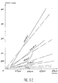
- FIGS. 5A to 5D show relationships, amplitude-time of rise of the electronic component for signals obtained in the case of a detector CdTe.
- a maximum amplitude is assigned to each straight or correlation curve.
- signal amplitude is proportional to energy of the photon ⁇ , it is possible to configure each of the curves by the energy of a ⁇ photon.
- FIG. 5A The results of FIG. 5A are obtained with a filtering constant (filter 62) of 0.5 ⁇ s.
- this time constant is 0.2 ⁇ s, 0.1 ⁇ s and 0.05 ⁇ s respectively.
- some curves obtained are not straight because the inability of the circuit to measure long times (greater than 0.4 ⁇ s). In all cases the estimate of the energy obtained is approximate ( ⁇ 5%).
- this signal is filtered to isolate the electronic component, and the maximum amplitude and the rise times of this electronic component are measures.
Landscapes
- Physics & Mathematics (AREA)
- Health & Medical Sciences (AREA)
- Life Sciences & Earth Sciences (AREA)
- General Physics & Mathematics (AREA)
- High Energy & Nuclear Physics (AREA)
- Molecular Biology (AREA)
- Spectroscopy & Molecular Physics (AREA)
- Measurement Of Radiation (AREA)
- Light Receiving Elements (AREA)
Claims (10)
- Verfahren zur Detektion von Gammastrahlung, das die Bildung einer Vielzahl von Signalen oder einer Vielzahl von Datengruppen umfasst, repräsentativ für die zeitliche Entwicklung eines Signals, das von einem Detektor aus Halbleitermaterial geliefert wird, wobei jedes Signal oder jede Datengruppe, geliefert durch den Detektor als Reaktion auf die Wechselwirkung der Gammastrahlung mit dem Halbleitermaterial, eine eine Elektronen-Sammlung betreffende Elektronen-Komponente und eine eine Löcher-Sammlung betreffende Löcher-Komponente enthält,
dadurch gekennzeichnet, dass es umfasst:für jedes Signal oder jede Datengruppe die Bildung einer Größe oder eines Signals, repräsentativ für die Anstiegszeit der Elektronen-Komponente, und die Bildung eines Signals, repräsentativ für entweder eine aus der Elektronen- und Löcher-Sammlung resultierende detektierte Gesamtaufladung oder einen Teil der detektierten Gesamtaufladung, der nur aus der Elektronen-Sammlung resultiert, unddas Herstellen einer Relation oder Korrelation zwischen einerseits einer ersten, die Anstiegszeiten der Elektronen-Komponenten repräsentierenden Datengruppe und andrerseits einer zweiten Datengruppe, die entweder die detektierten Gesamtaufladungen repräsentiert oder die Teile der Gesamtaufladungen, die nur aus der Elektronen-Sammlung resultieren. - Detektionsverfahren nach Anspruch 1, bei dem eine Größe oder ein Signal festgelegt bzw. ermittelt oder auch erzeugt wird, die oder das repräsentativ ist für die maximale elektronische Aufladung oder für die wenigstens einem Teil der ersten und zweiten Datengruppe entsprechende maximale Aufladung.
- Detektionsverfahren nach Anspruch 1 oder 2, dadurch gekennzeichnet, dass es die Ermittlung bzw. Festlegung einer maximalen Aufladung umfasst, aufgrund:von Signalen oder Daten bezüglich der Anstiegszeit der Elektronen-Komponenten und bezüglich der detektierten Gesamtaufladungen oder bezüglich Teilen der detektierten Gesamtaufladungen, die aus der Elektronen-Sammlung resultieren, undder genannten Relation oder Korrelation.
- Verfahren nach Anspruch 3, dadurch gekennzeichnet, dass es einen Schritt zur Korrektur einer detektierten Gesamtladung umfasst, aufgrund:der ermittelten bzw. festgelegten maximalen Aufladung,der der maximalen Aufladung entsprechenden Anstiegszeit, undder Anstiegszeit der Elektronen-Komponente.
- Detektionsverfahren nach Anspruch 1, dadurch gekennzeichnet, dass es die Bildung eines Signals umfasst, das entweder für die Amplitude eines Signals repräsentativ ist, das eine Elektronen-Komponente und eine Löcher-Komponente umfasst, oder für die Amplitude eines Signals, das nur eine Elektronen-Komponente umfasst.
- Gammastrahlungsdetektor, der Einrichtungen umfasst, um als Reaktion auf die Wechselwirkung einer Gammastrahlung mit einem Halbleitermaterial eine Vielzahl von Signalen oder von Datengruppen zu bilden, repräsentativ für die zeitliche Entwicklung eines Signals, wobei jedes Signal oder jede Datengruppe als Reaktion auf die Wechselwirkung der Gammastrahlung mit dem Halbleitermaterial eine eine Elektronen-Sammlung betreffende Elektronen-Komponente oder eine eine Löcher-Sammlung betreffende Löcher-Komponente enthält,
dadurch gekennzeichnet, dass er umfasst:für jedes Signal oder jede Datengruppe Einrichtungen (38, 68, 70, 72) zur Bildung einer Größe oder eines Signals, repräsentativ für die Anstiegszeit der Elektronen-Komponente, und Einrichtungen (34, 36, 64, 65, 80, 81) zur Bildung eines Signals, das repräsentativ ist für entweder eine aus der Elektronen- und Löcher-Sammlung resultierende detektierte Gesamtaufladung oder einen Teil der detektierten Gesamtaufladung, der nur aus der Elektronen-Sammlung resultiert, undEinrichtungen zum Herstellen einer Relation, oder Korrelation, zwischen einerseits einer ersten, die Anstiegszeiten der elektronischen Komponenten bzw. Elektronen-Komponenten repräsentierenden Datengruppe, und andrerseits einer zweiten Datengruppe, die entweder die detektierten Gesamtaufladungen repräsentiert oder die Teile der Gesamtaufladungen, die nur aus der Elektronen-Sammlung resultieren. - Detektor nach Anspruch 6, der außerdem Einrichtungen umfasst, um ein Signal oder eine Größe zur erzeugen, repräsentativ für die maximale elektronische Aufladung oder für die wenigstens einem Teil der ersten und zweiten Datengruppe entsprechende maximale Aufladung.
- Detektor nach Anspruch 6 oder 7, dadurch gekennzeichnet, dass es Einrichtungen zur Ermittlung bzw. Festlegung einer maximalen Aufladung umfasst, aufgrund:von Signalen oder Daten bezüglich der Anstiegszeit der Elektronen-Komponenten und bezüglich der detektierten Gesamtaufladungen oder bezüglich Teilen der detektierten Gesamtaufladungen, die aus der Elektronen-Sammlung resultieren, undder genannten Relation oder Korrelation.
- Verfahren nach Anspruch 8, dadurch gekennzeichnet, dass es Einrichtungen zur Korrektur einer detektierten Gesamtladung umfasst, aufgrund:der ermittelten bzw. festgelegten maximalen Aufladung,der der maximalen Aufladung entsprechenden Anstiegszeit, undder Anstiegszeit der Elektronen-Komponente.
- Detektor nach Anspruch 6, dadurch gekennzeichnet, dass es Einrichtungen zur Bildung eines Signals umfasst, das entweder für die Amplitude eines Signals repräsentativ ist, das eine Elektronen-Komponente und eine Löcher-Komponente umfasst, oder für die Amplitude eines Signals, das nur eine Elektronen-Komponente umfasst.
Applications Claiming Priority (2)
| Application Number | Priority Date | Filing Date | Title |
|---|---|---|---|
| FR9510849A FR2738919B1 (fr) | 1995-09-15 | 1995-09-15 | Procede et dispositif pour la correction de mesure spectrometrique dans le domaine de la detection de photons gamma |
| FR9510849 | 1995-09-15 |
Publications (2)
| Publication Number | Publication Date |
|---|---|
| EP0763751A1 EP0763751A1 (de) | 1997-03-19 |
| EP0763751B1 true EP0763751B1 (de) | 2002-01-09 |
Family
ID=9482599
Family Applications (1)
| Application Number | Title | Priority Date | Filing Date |
|---|---|---|---|
| EP96401963A Expired - Lifetime EP0763751B1 (de) | 1995-09-15 | 1996-09-13 | Verfahren und Vorrichtung zur Korrektur von Signalen in der Gammaphotonenspektroskopie |
Country Status (6)
| Country | Link |
|---|---|
| US (1) | US5854489A (de) |
| EP (1) | EP0763751B1 (de) |
| JP (1) | JP3961052B2 (de) |
| CA (1) | CA2185302A1 (de) |
| DE (1) | DE69618406T2 (de) |
| FR (1) | FR2738919B1 (de) |
Families Citing this family (29)
| Publication number | Priority date | Publication date | Assignee | Title |
|---|---|---|---|---|
| FR2767387B1 (fr) * | 1997-08-14 | 1999-10-01 | Commissariat Energie Atomique | Dispositif pour la mesure spectrometrique dans le domaine de la detection de photons gamma |
| FR2769099B1 (fr) * | 1997-10-01 | 1999-11-05 | Commissariat Energie Atomique | Dispositif de mesure du temps de montee de signaux parasites par des bruits, provenant de detecteurs de rayonnements y ou x |
| FR2790560B1 (fr) | 1999-03-05 | 2001-04-13 | Commissariat Energie Atomique | Procede et dispositif de tri en temps reel d'evenements de detection d'un detecteur de rayonnements gamma et de correction d'uniformite d'elements de detection du detecteur |
| AU2000274441A1 (en) * | 2000-09-25 | 2002-04-08 | Hamamatsu Photonics K.K. | Optical measurement apparatus and method for optical measurement |
| FR2815132B1 (fr) * | 2000-10-10 | 2002-11-29 | Commissariat Energie Atomique | Procede de traitement d'un spectre en energie de rayonnements gamma |
| FR2819054B1 (fr) * | 2000-12-28 | 2003-09-26 | Commissariat Energie Atomique | Procedes et appareils pour le traitement analogique du signal emis par un detecteur de particules |
| JP2005049144A (ja) * | 2003-07-30 | 2005-02-24 | Toshiba Corp | 放射線計測方法 |
| JP4619640B2 (ja) * | 2003-10-10 | 2011-01-26 | 富士フイルム株式会社 | 信号検出方法および装置 |
| FR2868545B1 (fr) | 2004-03-31 | 2006-05-19 | Commissariat Energie Atomique | Systeme d'acquisition de spectres avec integrateur a adaptation de seuil. |
| FR2869692B1 (fr) * | 2004-05-03 | 2006-06-23 | Commissariat Energie Atomique | Procede de correction des spectres bi-parametriques |
| FR2872921B1 (fr) * | 2004-07-09 | 2006-09-15 | Commissariat Energie Atomique | Dispositif et procede de mesure de l'energie et de la position d'une particule incidente dans un detecteur |
| US7820977B2 (en) | 2005-02-04 | 2010-10-26 | Steve Beer | Methods and apparatus for improved gamma spectra generation |
| US7847260B2 (en) | 2005-02-04 | 2010-12-07 | Dan Inbar | Nuclear threat detection |
| US8173970B2 (en) | 2005-02-04 | 2012-05-08 | Dan Inbar | Detection of nuclear materials |
| JP4611106B2 (ja) | 2005-03-11 | 2011-01-12 | 住友重機械工業株式会社 | 放射線検出回路及び放射線検査装置 |
| JP4670704B2 (ja) * | 2006-03-31 | 2011-04-13 | 株式会社日立製作所 | エネルギー較正方法,エネルギー関心領域の設定方法、放射線検出装置及び核医学診断装置 |
| WO2008054883A2 (en) * | 2006-06-07 | 2008-05-08 | Xrf Corporation | Devices and methods for detecting and analyzing radiation |
| FR2905766B1 (fr) | 2006-09-08 | 2011-09-30 | Ixsea | Sonar a antenne deformable et procede associe de traitement du signal pour former une antenne synthetique |
| JP2010507090A (ja) | 2006-10-20 | 2010-03-04 | コミサリア、ア、レネルジ、アトミク−セーエーアー | 検出器における相互作用深度を用いるガンマカメラ |
| JP4814808B2 (ja) * | 2007-02-05 | 2011-11-16 | 株式会社日立製作所 | 核医学撮像装置 |
| CN101470207A (zh) * | 2007-12-29 | 2009-07-01 | 同方威视技术股份有限公司 | 多道脉冲分析器及峰飘实时修正方法 |
| WO2010133871A2 (en) * | 2009-05-19 | 2010-11-25 | Durham Scientific Crystals Limited | Radiation detection |
| FR2950979B1 (fr) | 2009-10-07 | 2012-12-07 | Commissariat Energie Atomique | Procede de traitement de donnees issues d'un detecteur de rayonnements ionisants |
| CN101776577B (zh) * | 2010-02-26 | 2011-04-13 | 浙江大学 | 一种植物营养含量检测光谱仪的校正方法 |
| JP5661325B2 (ja) | 2010-04-20 | 2015-01-28 | 株式会社東芝 | X線ct装置 |
| EP3049828A4 (de) * | 2013-09-27 | 2017-06-07 | Saint-Gobain Ceramics&Plastics, Inc. | Analysator zur kompensation eines szintillators und verfahren zur verwendung davon |
| FR3058230B1 (fr) * | 2016-10-27 | 2019-03-15 | Detection Technology Sas | Dispositif de spectrometrie |
| JP7079748B2 (ja) * | 2019-03-14 | 2022-06-02 | 株式会社堀場製作所 | 放射線検出装置及び放射線検出用信号処理装置 |
| CA3115634A1 (en) * | 2021-04-20 | 2022-10-20 | Rodney HERRING | Charged particle imaging system and use thereof |
Family Cites Families (1)
| Publication number | Priority date | Publication date | Assignee | Title |
|---|---|---|---|---|
| EP0167119B1 (de) * | 1984-06-30 | 1991-10-23 | Shimadzu Corporation | Halbleiterstrahlungsdetektor |
-
1995
- 1995-09-15 FR FR9510849A patent/FR2738919B1/fr not_active Expired - Lifetime
-
1996
- 1996-09-11 CA CA002185302A patent/CA2185302A1/en not_active Abandoned
- 1996-09-13 EP EP96401963A patent/EP0763751B1/de not_active Expired - Lifetime
- 1996-09-13 DE DE69618406T patent/DE69618406T2/de not_active Expired - Lifetime
- 1996-09-13 US US08/713,630 patent/US5854489A/en not_active Expired - Lifetime
- 1996-09-13 JP JP24387396A patent/JP3961052B2/ja not_active Expired - Fee Related
Also Published As
| Publication number | Publication date |
|---|---|
| FR2738919B1 (fr) | 1997-10-17 |
| DE69618406D1 (de) | 2002-02-14 |
| EP0763751A1 (de) | 1997-03-19 |
| JPH09127249A (ja) | 1997-05-16 |
| DE69618406T2 (de) | 2002-08-29 |
| JP3961052B2 (ja) | 2007-08-15 |
| FR2738919A1 (fr) | 1997-03-21 |
| US5854489A (en) | 1998-12-29 |
| CA2185302A1 (en) | 1997-03-16 |
Similar Documents
| Publication | Publication Date | Title |
|---|---|---|
| EP0763751B1 (de) | Verfahren und Vorrichtung zur Korrektur von Signalen in der Gammaphotonenspektroskopie | |
| EP1004040B1 (de) | Vorrichtung zur spektrometrischen messung im gebiet der detektion von gammaphotonen | |
| EP1704422B1 (de) | Detektionsgerät zur strahlunsmessung durch zählung von impulsen mit doppelter rücksetzschaltung | |
| EP2507652B1 (de) | Verfahren zur kalibrierung eines röntgendetektors | |
| EP2541280B1 (de) | Vorrichtung zur Erfassung von ionisierender Strahlung mit einem Halbleiterdetektor mit verbesserter spektrometrischer Ansprache | |
| EP0762145B1 (de) | Pulsverarbeitungssystem für einen Gammateilchen-CdTe-Strahlungsdetektor | |
| FR2757685A1 (fr) | Dispositif de detection de rayonnements ionisants a semi-conducteur de haute resistivite | |
| EP3432035B1 (de) | Verfahren und elektronisches zirkuit zur verarbeitung von von einem ionisierenden strahlungsdetektor generierten puls | |
| EP1565763B1 (de) | Verbesserte schaltungsanordnung für spektrometrie und spektrometrisches system, das diese anordnung verwendet | |
| EP0907086B1 (de) | Vorrichtung zum Messen der Aufsteigszeit von verrauschten Signalen von Gamma- oder Röntgendetektoren | |
| CA2736593C (fr) | Systeme de controle de derive de gain de photomultiplicateur et procede associe | |
| EP2962129B1 (de) | Vorrichtung zur verarbeitung eines strahlungsdetektorsignals | |
| EP2936208B1 (de) | Auf halbleiterdetektor basierendes verfahren und vorrichtung zur erfassung ionisierender strahlung | |
| FR2666170A1 (fr) | Imageur haute resolution a bas niveau de lumiere. | |
| EP1402285B1 (de) | Gerät zur verminderung der verschmierung und des dunkelstroms bei einem teilchendetektor, insbesondere bei einem photonendetektor | |
| WO2006059035A1 (fr) | Detecteur de neutrons a semi-conducteur | |
| EP1058128A1 (de) | Verfahren und Vorrichtung zur Unterscheidung von Impulsen von Halbleiter-Strahlungsdetektoren | |
| FR2945668A1 (fr) | Capteur d'image pour imagerie a tres bas niveau de lumiere. | |
| CA2203413A1 (fr) | Semiconductor x ray detector | |
| WO2010084280A1 (fr) | Structure d'amplification et chaîne de détection et de mesure comportant une telle structure |
Legal Events
| Date | Code | Title | Description |
|---|---|---|---|
| PUAI | Public reference made under article 153(3) epc to a published international application that has entered the european phase |
Free format text: ORIGINAL CODE: 0009012 |
|
| AK | Designated contracting states |
Kind code of ref document: A1 Designated state(s): DE FI GB IT |
|
| 17P | Request for examination filed |
Effective date: 19970823 |
|
| 17Q | First examination report despatched |
Effective date: 20000608 |
|
| GRAG | Despatch of communication of intention to grant |
Free format text: ORIGINAL CODE: EPIDOS AGRA |
|
| RTI1 | Title (correction) |
Free format text: METHOD AND APPARATUS FOR CORRECTING SIGNALS IN GAMMA PHOTON SPECTROSCOPY |
|
| GRAG | Despatch of communication of intention to grant |
Free format text: ORIGINAL CODE: EPIDOS AGRA |
|
| GRAH | Despatch of communication of intention to grant a patent |
Free format text: ORIGINAL CODE: EPIDOS IGRA |
|
| GRAG | Despatch of communication of intention to grant |
Free format text: ORIGINAL CODE: EPIDOS AGRA |
|
| GRAH | Despatch of communication of intention to grant a patent |
Free format text: ORIGINAL CODE: EPIDOS IGRA |
|
| GRAH | Despatch of communication of intention to grant a patent |
Free format text: ORIGINAL CODE: EPIDOS IGRA |
|
| GRAA | (expected) grant |
Free format text: ORIGINAL CODE: 0009210 |
|
| REG | Reference to a national code |
Ref country code: GB Ref legal event code: IF02 |
|
| AK | Designated contracting states |
Kind code of ref document: B1 Designated state(s): DE FI GB IT |
|
| PG25 | Lapsed in a contracting state [announced via postgrant information from national office to epo] |
Ref country code: FI Free format text: LAPSE BECAUSE OF FAILURE TO SUBMIT A TRANSLATION OF THE DESCRIPTION OR TO PAY THE FEE WITHIN THE PRESCRIBED TIME-LIMIT Effective date: 20020109 |
|
| REF | Corresponds to: |
Ref document number: 69618406 Country of ref document: DE Date of ref document: 20020214 |
|
| GBT | Gb: translation of ep patent filed (gb section 77(6)(a)/1977) |
Effective date: 20020404 |
|
| PLBE | No opposition filed within time limit |
Free format text: ORIGINAL CODE: 0009261 |
|
| STAA | Information on the status of an ep patent application or granted ep patent |
Free format text: STATUS: NO OPPOSITION FILED WITHIN TIME LIMIT |
|
| 26N | No opposition filed | ||
| PGFP | Annual fee paid to national office [announced via postgrant information from national office to epo] |
Ref country code: IT Payment date: 20130923 Year of fee payment: 18 |
|
| PGFP | Annual fee paid to national office [announced via postgrant information from national office to epo] |
Ref country code: DE Payment date: 20140911 Year of fee payment: 19 |
|
| PGFP | Annual fee paid to national office [announced via postgrant information from national office to epo] |
Ref country code: GB Payment date: 20140917 Year of fee payment: 19 |
|
| PG25 | Lapsed in a contracting state [announced via postgrant information from national office to epo] |
Ref country code: IT Free format text: LAPSE BECAUSE OF NON-PAYMENT OF DUE FEES Effective date: 20140913 |
|
| REG | Reference to a national code |
Ref country code: DE Ref legal event code: R119 Ref document number: 69618406 Country of ref document: DE |
|
| GBPC | Gb: european patent ceased through non-payment of renewal fee |
Effective date: 20150913 |
|
| PG25 | Lapsed in a contracting state [announced via postgrant information from national office to epo] |
Ref country code: DE Free format text: LAPSE BECAUSE OF NON-PAYMENT OF DUE FEES Effective date: 20160401 Ref country code: GB Free format text: LAPSE BECAUSE OF NON-PAYMENT OF DUE FEES Effective date: 20150913 |