EP0321759B1 - Electromagnetic shock waves source - Google Patents
Electromagnetic shock waves source Download PDFInfo
- Publication number
- EP0321759B1 EP0321759B1 EP88120217A EP88120217A EP0321759B1 EP 0321759 B1 EP0321759 B1 EP 0321759B1 EP 88120217 A EP88120217 A EP 88120217A EP 88120217 A EP88120217 A EP 88120217A EP 0321759 B1 EP0321759 B1 EP 0321759B1
- Authority
- EP
- European Patent Office
- Prior art keywords
- membrane
- diaphragm
- wave source
- shock
- copper
- Prior art date
- Legal status (The legal status is an assumption and is not a legal conclusion. Google has not performed a legal analysis and makes no representation as to the accuracy of the status listed.)
- Expired - Lifetime
Links
Images

Classifications
-
- G—PHYSICS
- G10—MUSICAL INSTRUMENTS; ACOUSTICS
- G10K—SOUND-PRODUCING DEVICES; METHODS OR DEVICES FOR PROTECTING AGAINST, OR FOR DAMPING, NOISE OR OTHER ACOUSTIC WAVES IN GENERAL; ACOUSTICS NOT OTHERWISE PROVIDED FOR
- G10K9/00—Devices in which sound is produced by vibrating a diaphragm or analogous element, e.g. fog horns, vehicle hooters or buzzers
- G10K9/12—Devices in which sound is produced by vibrating a diaphragm or analogous element, e.g. fog horns, vehicle hooters or buzzers electrically operated
Definitions
- the invention relates to an electromagnetic shock wave source as is known from DE-A-35 05 894.
- Electromagnetic shock wave generation is used, among other things, in extracorporeal stone crushing (DE 33 28 066 A) and is also suitable for other therapeutic methods in which shock waves are used.
- shock tube In the magazine "Akustician Beihefte", 1962, Issue 1, pages 158 to 202, the structure of a so-called shock tube is described.
- a copper membrane is located in front of a flat coil, separated by an insulating film.
- a tube filled with water connects to this copper membrane.
- a voltage in the range of 2 - 20 kV to the flat coil, a magnetic field is induced in the copper membrane, which causes repulsive forces that push the membrane away from the coil.
- Such a shock tube is used, for example, for chemical substance testing.
- EP 212 352 A1 discloses an ultrasound generator which contains a piezoelectric transducer which is constructed from a plurality of active layers and contains two lead plates for electrical contacting and for acoustic coupling.
- a lithotripter with a generic electromagnetic shock wave source is known from EP 278 304 A1.
- the shock wave source contains a base body, a wire coil, an insulation film and a copper membrane. This latter document can only be used to assess novelty, in accordance with Article 54 (3) EPC.
- DE-A-35 05 894 describes a shock tube which comprises a coil. There is an insulating film on both sides of the coil. A membrane made of electrically conductive material connects to the insulating film.
- the object of the invention is to improve such a shock wave source in such a way that efficiency and service life are increased.
- the preferred metals used are stainless steel for the high-strength membrane and copper or silver for the highly conductive membranes.
- Preferred dimensions are: Noble jet membrane: 0.1 - 0.2 mm Copper membrane: 0.05 - 0.2 mm Insulation film: 0.025 - 0.125 mm
- any number of combinations are possible in the number and thickness of the insulating foils or metal membranes. However, a total thickness of up to 1 mm should not be exceeded.
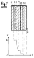
- the shock wave source according to the invention here consists of a basic body 1, a wire coil 2, an insulation film 3, a copper membrane 4, a further insulation film 5, a second copper membrane 6, a further insulation film 7 and a stainless steel membrane 8, which is grounded. Designs with more than two highly conductive metal foils 4, 6 are possible, but not shown.
- the individual layers are connected to one another in a conventional manner, for example by gluing.
- the figure shows the shock wave source on a greatly enlarged scale. A total thickness of up to 1.0 mm is realistic.
- the potential curve U is shown during the application of a high voltage.
- the coil 2 is at the high potential U0.
- the stainless steel membrane 8 is at earth potential.
- the copper membranes 4 and 6 are each at potentials that lie between the value U0 and 0. Within the insulation foils 3, 5 and 7, the potential U falls from the higher value to a lower one.
- FIG. 2 shows the current density distribution in a 0.2 mm thick copper membrane and the current density distribution in two 0.1 mm thick copper membranes, which are separated by an insulation film. Due to the skin effect, the current density at high frequencies is not evenly distributed over the conductor cross-section. The maximum depth of penetration at the frequency used is approx. 0.2 mm.
- the distribution of the current density is shown schematically in FIG. 2. As can be seen from this, the integral over the current density is larger when using two membranes. This increases the repulsive forces and the amplitude of the pressure pulse generated. In the case of well-conductive membranes whose thicknesses are greater than 0.4 mm, the current density is zero in the inner region. This is not the case with a layered membrane. The distribution of the current density is similar in each membrane.
Landscapes
- Physics & Mathematics (AREA)
- Engineering & Computer Science (AREA)
- Acoustics & Sound (AREA)
- Multimedia (AREA)
- Surgical Instruments (AREA)
- Building Environments (AREA)
Description
Die Erfindung betrifft eine elektromagnetische Stosswellenquelle wie sie aus DE-A-35 05 894 bekannt ist.The invention relates to an electromagnetic shock wave source as is known from DE-A-35 05 894.
Die elektromagnetische Stosswellenerzeugung (EMSE) wird unter anderem bei der extrakorporalen Steinzerkleinerung eingesetzt (DE 33 28 066 A) und ist auch für andere therapeutische Verfahren geeignet, bei denen Stosswellen verwendet werden.Electromagnetic shock wave generation (EMSE) is used, among other things, in extracorporeal stone crushing (DE 33 28 066 A) and is also suitable for other therapeutic methods in which shock waves are used.
In der Zeitschrift "Akustische Beihefte", 1962, Heft 1, Seiten 158 bis 202, ist der Aufbau eines sogenannten Stosswellenrohres beschrieben. Vor einer Flachspule, durch eine Isolierfolie getrennt, befindet sich eine Kupfermembran. An dieser Kupfermembran schliesst ein mit Wasser gefülltes Rohr an. Durch Anlegen einer Spannung im Bereich von 2 - 20 kV an die Flachspule wird in der Kupfermembran ein Magnetfeld induziert, welches Abstosskräfte bewirkt, die die Membran von der Spule wegdrücken. Hierdurch entsteht ein ebener Druckpuls, der im wassergefüllten Rohr zu einer steilen Stosswelle wird und am Rohrende für Experimente zur Verfügung steht. Eingesetzt wird ein solches Stosswellenrohr zum Beispiel zu Stoffuntersuchungen in der Chemie.In the magazine "Akustische Beihefte", 1962,
Aus der EP 212 352 A1 ist ein Ultraschallgenerator bekannt, der einen piezoelektrischen Wandler enthält, der aus mehreren aktiven Schichten aufgebaut ist und zwei Bleiplatten zur elektrischen Kontaktierung und zur akustischen Ankoppelung enthält.EP 212 352 A1 discloses an ultrasound generator which contains a piezoelectric transducer which is constructed from a plurality of active layers and contains two lead plates for electrical contacting and for acoustic coupling.
Aus der EP 278 304 A1 ist ein Lithotripter mit einer gattungsgemäßen elektromagnetischen Stosswellenquelle bekannt. Die Stosswellenquelle enthält einen Grundkörper, eine Drahtspule, eine Isolationsfolie und eine Kupfermembran. Diese letzgenannte Schrift ist nur zur Beurteilung der Neuheit heranzuziehen, gemäß Artikel 54(3) EPÜ.A lithotripter with a generic electromagnetic shock wave source is known from EP 278 304 A1. The shock wave source contains a base body, a wire coil, an insulation film and a copper membrane. This latter document can only be used to assess novelty, in accordance with Article 54 (3) EPC.
In der DE-A-35 05 894 ist ein Stosswellenrohr beschrieben, das eine Spule umfaßt. Auf beiden Selten der Spule befindet sich je eine Isolierfolie. An die Isolierfolie schließt sich jeweils eine Membran aus elektrisch leitfähigem Material an.DE-A-35 05 894 describes a shock tube which comprises a coil. There is an insulating film on both sides of the coil. A membrane made of electrically conductive material connects to the insulating film.
Aufgabe der Erfindung ist es, eine solche Stosswellenquelle dahingehend zu verbessern, dass Wirkungsgrad und Lebensdauer erhöht werden.The object of the invention is to improve such a shock wave source in such a way that efficiency and service life are increased.
Diese Aufgabe wird erfindungsgemäß gelöst von einer Stosswellenquelle mit den Merkmalen des Anspruchs 1. Ausführungen der Erfindung sind Gegenstände von Unteransprüchen.This object is achieved according to the invention by a shock wave source with the features of
Die Erfindung hat folgende Vorteile:
- Wirkungsgradverluste durch eine geerdete Kupfermembran werden vermieden. Die Erwärmung des Gesamtsystems wird wegen des verbesserten Wirkungsgrades verringert.
- Der Skineffekt wirkt sich nicht mehr begrenzend auf die gesamte Dicke der gut leitfähigen Membran aus, wie anhand von
Figur 2 gezeigt ist. Dennoch können nun mehrere Membranen hintereinander gesetzt werden, deren Gesamtdicke größer ist als die einer einzelnen Membran. - Die Potentialaufteilung zwischen Spule und der geerdeten abschliessenden Metallmembran wird günstiger, da die zwischenliegenden Membranen gegen die abschliessende Metallmembran isoliert sind und deshalb beim Anlegen einer hohen Spannung ein bestimmtes, niedrigeres Potential annehmen. Dies erhöht die Lebensdauer, denn die Lebensdauer des Systems ist bestimmt durch die Durchschlagfestigkeit der Isolationsschicht zwischen Drahtspule und Membran. Aufgrund der günstigeren Potentialaufteilung wird die Isolationsschicht elektrisch weniger stark beansprucht, das heisst die Lebensdauer erhöht sich.
- Die gut leitfähigen Membrane können direkt auf die Spule aufgelegt werden, sofern die Isolationsschicht zwischen ihren und der abschliessenden Membran entsprechend ausgelegt ist. Hieraus folgt eine weitere Verbesserung der Ankopplung der Membran an die Drahtspule, da das Streufeld minimiert wird.
- Verringerung der Wirbelstromverluste.
- Efficiency losses due to an earthed copper membrane are avoided. The heating of the overall system is reduced due to the improved efficiency.
- The skin effect no longer has a limiting effect on the entire thickness of the highly conductive membrane, as shown in FIG. 2. Nevertheless, several membranes can now be placed one behind the other, the total thickness of which is greater than that of a single membrane.
- The potential distribution between the coil and the grounded, final metal membrane becomes more favorable because the membranes in between are isolated from the final metal membrane and therefore assume a certain, lower potential when a high voltage is applied. This increases the lifespan, because the lifespan of the system is determined by the dielectric strength of the insulation layer between the wire coil and the membrane. Due to the more favorable potential distribution, the insulation layer is subjected to less electrical stress, which means that the service life increases.
- The highly conductive membrane can be placed directly on the coil, provided the insulation layer between its and the final membrane is designed accordingly is. This results in a further improvement in the coupling of the membrane to the wire coil, since the stray field is minimized.
- Reduction of eddy current losses.
Als bevorzugte Metalle werden für die hochfeste Membran Edelstahl und für die gut leitfähigen Membranen Kupfer oder Silber verwendet.The preferred metals used are stainless steel for the high-strength membrane and copper or silver for the highly conductive membranes.
Bevorzugte Dimensionen sind:
In der Anzahl und Dicke der Isolationsfolien oder der Metallmembranen sind beliebige Kombinationen möglich. Allerdings sollte eine Gesamtdicke von bis zu 1 mm nicht überschritten werden.Any number of combinations are possible in the number and thickness of the insulating foils or metal membranes. However, a total thickness of up to 1 mm should not be exceeded.
Die Erfindung wird anhand zweier Figuren näher erläutert.
Figur 1- zeigt eine erfindungsgemässe Stosswellenquelle,
Figur 2- zeigt den Stromdichteverlauf in verschiedenen Membranen.
- Figure 1
- shows a shock wave source according to the invention,
- Figure 2
- shows the current density curve in different membranes.
Die Figur 1 zeigt in ihrer oberen Hälfte den Aufbau einer bevorzugten Ausführungsform einer erfindungsgemässen Stosswellenquelle und in ihrer unteren Hälfte den Potentialverlauf beim Anlegen einer hohen Spannung an die Spule.
Die erfindungsgemässe Stosswellenquelle besteht hier aus einem Grundköprer 1, einer Drahtspule 2, einer Isolationsfolie 3, einer Kupfermembran 4, einer weiteren Isolationsfolie 5, einer zweiten Kupfermembran 6, einer weiteren Isolationsfolie 7 und eine Edelstahlmembran 8, die geerdet ist. Möglich, aber nicht gezeigt, sind Ausführungen mit mehr als zwei gut leitenden Metallfolien 4, 6. Die einzelnen Schichten sind auf konventionelle Weise, zum Beispiel durch Kleben, miteinander verbunden.
Die Figur zeigt die Stosswellenquelle in stark vergrössertem Maßstab. Realistisch ist eine Gesamtdicke bis zu 1,0 mm.
Im unteren Teil der Figur ist der Potentialverlauf U während des Anlegens einer hohen Spannung gezeigt. Die Spule 2 liegt auf dem hohen Potential U₀. Die Edelstahlmembran 8 liegt auf Erdpotential.
Die Kupfermembranen 4 und 6 liegen jeweils auf Potentialen, die zwischen dem Wert U₀ und 0 liegen. Innerhalb der Isolationsfolien 3, 5 und 7 fällt das Potential U jeweils vom höheren Wert auf einen niedrigeren.1 shows in its upper half the structure of a preferred embodiment of a shock wave source according to the invention and in its lower half the potential curve when a high voltage is applied to the coil.
The shock wave source according to the invention here consists of a
The figure shows the shock wave source on a greatly enlarged scale. A total thickness of up to 1.0 mm is realistic.
In the lower part of the figure, the potential curve U is shown during the application of a high voltage. The
The
Figur 2 zeigt oben die Stromdichteverteilung in einer 0,2 mm dicken Kupfermembran und unten die Stromdichteverteilung in zwei 0,1 mm dicken Kupfermembranen, die von einer Isolationsfolie getrennt sind. Aufgrund des Skineffektes verteilt sich die Stromdichte bei hohen Frequenzen nicht gleichmässig über den Leiterquerschnitt. Die maximale Eindringtiefe bei der verwendeten Frequenz beträgt ca. 0,2 mm. Die Verteilung der Stromdichte ist schematisch in der Figur 2 gezeigt.
Wie daraus ersichtlich wird, ist das Integral über die Stromdichte bei Verwendung zweier Membranen grösser. Damit erhöhen sich die Abstossungskräfte und die Amplitude des erzeugten Druckimpules.
Bei gut leitfähigen Membranen, deren Dicken grösser als 0,4 mm sind, ist im inneren Bereich die Stromdichte Null. Bei einer geschichteten Membran ist dies nicht der Fall. Die Verteilung der Stromdichte ist in jeder Membran ähnlich.FIG. 2 shows the current density distribution in a 0.2 mm thick copper membrane and the current density distribution in two 0.1 mm thick copper membranes, which are separated by an insulation film. Due to the skin effect, the current density at high frequencies is not evenly distributed over the conductor cross-section. The maximum depth of penetration at the frequency used is approx. 0.2 mm. The distribution of the current density is shown schematically in FIG. 2.
As can be seen from this, the integral over the current density is larger when using two membranes. This increases the repulsive forces and the amplitude of the pressure pulse generated.
In the case of well-conductive membranes whose thicknesses are greater than 0.4 mm, the current density is zero in the inner region. This is not the case with a layered membrane. The distribution of the current density is similar in each membrane.
Claims (4)
- Shock-wave source comprising a base body (1), at least one wire coil (2), an insulation foil (3) and a first metal diaphragm (8), as well as at least one additional metal diaphragm (4, 6) of good conductivity, which is separated from the first metal diaphragm (8) by at least one insulation foil (7) and highly rigid, and that the at least one additional metal diaphragm (4, 6) of good conductivity is provided between the coil (2) and the first metal diaphragm (8), and that furthermore an insulation foil (5) is provided between each additional metal diaphragm (4, 6).
- Shock waves according to claim 1, characterised in that the metal diaphragms (4, 6) of good conductivity are made of copper or silver.
- Shock-wave source according to at least one of the above claims, characterised in that the highly rigid diaphragm (8) is made of stainless steel.
- Shock-wave source according to at least one of the above claims, characterised by the following materials and thicknesses:
- stainless steel diaphragm: 0.1 - 0.2 mm - insulation foil: 0.025 - 0.125 mm - copper diaphragm: 0.05 - 0.2 mm
Applications Claiming Priority (2)
| Application Number | Priority Date | Filing Date | Title |
|---|---|---|---|
| DE3743822 | 1987-12-23 | ||
| DE19873743822 DE3743822A1 (en) | 1987-12-23 | 1987-12-23 | ELECTROMAGNETIC SHAFT SOURCE |
Publications (3)
| Publication Number | Publication Date |
|---|---|
| EP0321759A2 EP0321759A2 (en) | 1989-06-28 |
| EP0321759A3 EP0321759A3 (en) | 1989-10-04 |
| EP0321759B1 true EP0321759B1 (en) | 1994-06-01 |
Family
ID=6343441
Family Applications (1)
| Application Number | Title | Priority Date | Filing Date |
|---|---|---|---|
| EP88120217A Expired - Lifetime EP0321759B1 (en) | 1987-12-23 | 1988-12-03 | Electromagnetic shock waves source |
Country Status (5)
| Country | Link |
|---|---|
| US (1) | US4924858A (en) |
| EP (1) | EP0321759B1 (en) |
| JP (1) | JPH0741043B2 (en) |
| DE (1) | DE3743822A1 (en) |
| ES (1) | ES2056880T3 (en) |
Families Citing this family (17)
| Publication number | Priority date | Publication date | Assignee | Title |
|---|---|---|---|---|
| DE3907605C2 (en) * | 1989-03-09 | 1996-04-04 | Dornier Medizintechnik | Shock wave source |
| DE4130796A1 (en) * | 1990-09-27 | 1992-04-02 | Siemens Ag | ELECTRICALLY DRIVABLE SHOCK WAVE SOURCE |
| US5233972A (en) * | 1990-09-27 | 1993-08-10 | Siemens Aktiengesellschaft | Shockwave source for acoustic shockwaves |
| DE4041063A1 (en) * | 1990-12-20 | 1992-06-25 | Siemens Ag | Removal of artificial joints - with focussed ultrasonic head to loosen cement around joint support |
| DE4125088C1 (en) * | 1991-07-29 | 1992-06-11 | Siemens Ag, 8000 Muenchen, De | |
| DE4201139A1 (en) * | 1992-01-17 | 1993-07-22 | Siemens Ag | ELECTROMAGNETIC ACOUSTIC PRESSURE PULSE SOURCE WITH ELECTRICALLY CONDUCTIVE MEMBRANES |
| DE4228963C2 (en) * | 1992-08-31 | 1998-10-22 | Siemens Ag | Pressure pulse source with a cavitation-resistant coated membrane |
| US7189209B1 (en) | 1996-03-29 | 2007-03-13 | Sanuwave, Inc. | Method for using acoustic shock waves in the treatment of a diabetic foot ulcer or a pressure sore |
| US6390995B1 (en) | 1997-02-12 | 2002-05-21 | Healthtronics Surgical Services, Inc. | Method for using acoustic shock waves in the treatment of medical conditions |
| DE10160595A1 (en) * | 2001-12-10 | 2003-06-26 | Dornier Medtech Holding Int Gmbh | Electromagnetic shock or pressure wave source |
| DE102004013573B3 (en) * | 2004-03-19 | 2005-09-01 | Dornier Medtech Systems Gmbh | Production of a traction impulse between electrically conducting structures comprises preparing the structures insulated from each other and lying next to each other, producing a magnetic field and switching off the magnetic field |
| DE102004036526B4 (en) * | 2004-07-28 | 2008-06-05 | Dornier Medtech Systems Gmbh | Shock wave source and shock wave treatment device |
| CN1878427A (en) * | 2005-06-07 | 2006-12-13 | 日本电产鸽株式会社 | Speaker |
| CN1882195A (en) * | 2005-06-07 | 2006-12-20 | 日本电产鸽株式会社 | Speaker |
| US9997189B2 (en) * | 2016-11-07 | 2018-06-12 | Seagate Technology Llc | Three dimensional electric field data storage device utilizing shockwaves and a light source |
| US10056146B2 (en) | 2016-11-07 | 2018-08-21 | Seagate Technology Llc | Electric field storage device |
| US20220072326A1 (en) * | 2020-09-10 | 2022-03-10 | Moshe Ein-Gal | Combined pulsed electromagnetic field and low intensity shockwave system and method |
Citations (1)
| Publication number | Priority date | Publication date | Assignee | Title |
|---|---|---|---|---|
| DE3505894A1 (en) * | 1985-02-20 | 1986-08-21 | Siemens AG, 1000 Berlin und 8000 München | Shock wave tube with coil and diaphragm |
Family Cites Families (6)
| Publication number | Priority date | Publication date | Assignee | Title |
|---|---|---|---|---|
| DE3447440A1 (en) * | 1984-12-27 | 1986-07-03 | Siemens AG, 1000 Berlin und 8000 München | SHOCK SHAFT PIPE FOR THE CRUSHING OF CONCRETE |
| US4718421A (en) * | 1985-08-09 | 1988-01-12 | Siemens Aktiengesellschaft | Ultrasound generator |
| EP0256203A1 (en) * | 1986-06-05 | 1988-02-24 | Siemens Aktiengesellschaft | Shock wave generator for the disintegration of concretions in a living body by non-contacting means |
| US4796608A (en) * | 1986-06-16 | 1989-01-10 | Siemens Aktiengesellschaft | Shock wave generator for an apparatus for non-contacting disintegration of calculi in the body of a life form |
| DE8627238U1 (en) * | 1986-10-06 | 1988-02-04 | Siemens AG, 1000 Berlin und 8000 München | Shock wave source |
| EP0278304A1 (en) * | 1987-02-04 | 1988-08-17 | Siemens Aktiengesellschaft | Lithotripter with an integrated positioning device |
-
1987
- 1987-12-23 DE DE19873743822 patent/DE3743822A1/en active Granted
-
1988
- 1988-12-03 ES ES88120217T patent/ES2056880T3/en not_active Expired - Lifetime
- 1988-12-03 EP EP88120217A patent/EP0321759B1/en not_active Expired - Lifetime
- 1988-12-19 US US07/286,965 patent/US4924858A/en not_active Expired - Lifetime
- 1988-12-23 JP JP63325698A patent/JPH0741043B2/en not_active Expired - Lifetime
Patent Citations (1)
| Publication number | Priority date | Publication date | Assignee | Title |
|---|---|---|---|---|
| DE3505894A1 (en) * | 1985-02-20 | 1986-08-21 | Siemens AG, 1000 Berlin und 8000 München | Shock wave tube with coil and diaphragm |
Also Published As
| Publication number | Publication date |
|---|---|
| ES2056880T3 (en) | 1994-10-16 |
| DE3743822C2 (en) | 1989-10-12 |
| DE3743822A1 (en) | 1989-07-13 |
| US4924858A (en) | 1990-05-15 |
| EP0321759A2 (en) | 1989-06-28 |
| JPH0741043B2 (en) | 1995-05-10 |
| EP0321759A3 (en) | 1989-10-04 |
| JPH01280451A (en) | 1989-11-10 |
Similar Documents
| Publication | Publication Date | Title |
|---|---|---|
| EP0321759B1 (en) | Electromagnetic shock waves source | |
| DE69635308T2 (en) | PIEZOELECTRIC TRANSFORMER | |
| EP0025092B1 (en) | Ultrasonic transducer assembly and process for its production | |
| DE69837416T2 (en) | Conductive back element for a composite transducer | |
| DE69231190T2 (en) | ACTIVE PANEL WITH HIGH TRANSMISSION DAMPING | |
| DE69710314T2 (en) | SOUND TRANSDUCER WITH SEVERAL ELEMENTS AND COMMON EARTH ELECTRODE | |
| DE3214789A1 (en) | DYNAMICALLY FOCUSING ULTRASONIC transducer | |
| EP0212352A1 (en) | Ultrasonic generator | |
| DE2915761A1 (en) | DEVICE FOR ULTRASONIC EXAMINATION OF AN OBJECT | |
| EP0006623A2 (en) | Ultrasonic transducer | |
| DE2824995A1 (en) | MULTICELLED X-RAY DETECTOR | |
| DE3443869A1 (en) | CONVERTER ARRANGEMENT FOR HYDROPHONES | |
| DE3215242A1 (en) | ULTRASONIC HEAD | |
| DE4130798A1 (en) | SHOCK WAVE SOURCE FOR ACOUSTIC SHOCK WAVES | |
| DE2139200A1 (en) | Surface wave converter | |
| DE3505894A1 (en) | Shock wave tube with coil and diaphragm | |
| DE3709533C2 (en) | ||
| DE4125088C1 (en) | ||
| DE3784078T2 (en) | ECHOGRAPHY CONVERTER WITH CONNECTOR. | |
| DE3019410A1 (en) | Ultrasound transducer for medical diagnostics or material testing - has numerous transducing elements and contacting simplified by using metal coated plastics foil for contacting | |
| EP1911401B1 (en) | Plate segment for a multi part patient support plate and an operating table | |
| DE68918871T2 (en) | METHOD AND DEVICE FOR THE BIDIMENSIONAL LOCALIZATION OF UNCHARGED PARTICLES, ESPECIALLY AT A LOW COUNTING RATE. | |
| DE2444023A1 (en) | ELECTROSTATIC CONVERTER | |
| DE3502770A1 (en) | METHOD FOR PRODUCING A FLAT COIL AND FLAT COIL FOR A SHOCK SHAFT PIPE | |
| EP0160821B1 (en) | Apparatus for reading a two-dimensional charge image using an array |
Legal Events
| Date | Code | Title | Description |
|---|---|---|---|
| PUAI | Public reference made under article 153(3) epc to a published international application that has entered the european phase |
Free format text: ORIGINAL CODE: 0009012 |
|
| AK | Designated contracting states |
Kind code of ref document: A2 Designated state(s): CH ES IT LI NL |
|
| PUAL | Search report despatched |
Free format text: ORIGINAL CODE: 0009013 |
|
| AK | Designated contracting states |
Kind code of ref document: A3 Designated state(s): CH ES IT LI NL |
|
| 17P | Request for examination filed |
Effective date: 19890908 |
|
| 17Q | First examination report despatched |
Effective date: 19920810 |
|
| GRAA | (expected) grant |
Free format text: ORIGINAL CODE: 0009210 |
|
| AK | Designated contracting states |
Kind code of ref document: B1 Designated state(s): CH ES IT LI NL |
|
| ITF | It: translation for a ep patent filed | ||
| REG | Reference to a national code |
Ref country code: ES Ref legal event code: FG2A Ref document number: 2056880 Country of ref document: ES Kind code of ref document: T3 |
|
| PLBE | No opposition filed within time limit |
Free format text: ORIGINAL CODE: 0009261 |
|
| STAA | Information on the status of an ep patent application or granted ep patent |
Free format text: STATUS: NO OPPOSITION FILED WITHIN TIME LIMIT |
|
| 26N | No opposition filed | ||
| PGFP | Annual fee paid to national office [announced via postgrant information from national office to epo] |
Ref country code: NL Payment date: 20071220 Year of fee payment: 20 Ref country code: ES Payment date: 20071227 Year of fee payment: 20 |
|
| PGFP | Annual fee paid to national office [announced via postgrant information from national office to epo] |
Ref country code: IT Payment date: 20071220 Year of fee payment: 20 Ref country code: CH Payment date: 20071224 Year of fee payment: 20 |
|
| REG | Reference to a national code |
Ref country code: CH Ref legal event code: PL |
|
| PG25 | Lapsed in a contracting state [announced via postgrant information from national office to epo] |
Ref country code: NL Free format text: LAPSE BECAUSE OF EXPIRATION OF PROTECTION Effective date: 20081203 |
|
| REG | Reference to a national code |
Ref country code: ES Ref legal event code: FD2A Effective date: 20081204 |
|
| PG25 | Lapsed in a contracting state [announced via postgrant information from national office to epo] |
Ref country code: ES Free format text: LAPSE BECAUSE OF EXPIRATION OF PROTECTION Effective date: 20081204 |