EP0320100A2 - Analogdigitalwandler - Google Patents
Analogdigitalwandler Download PDFInfo
- Publication number
- EP0320100A2 EP0320100A2 EP88309780A EP88309780A EP0320100A2 EP 0320100 A2 EP0320100 A2 EP 0320100A2 EP 88309780 A EP88309780 A EP 88309780A EP 88309780 A EP88309780 A EP 88309780A EP 0320100 A2 EP0320100 A2 EP 0320100A2
- Authority
- EP
- European Patent Office
- Prior art keywords
- flux
- superconducting
- lobe
- loop
- transformer
- Prior art date
- Legal status (The legal status is an assumption and is not a legal conclusion. Google has not performed a legal analysis and makes no representation as to the accuracy of the status listed.)
- Withdrawn
Links
Images

Classifications
-
- H—ELECTRICITY
- H03—ELECTRONIC CIRCUITRY
- H03M—CODING; DECODING; CODE CONVERSION IN GENERAL
- H03M1/00—Analogue/digital conversion; Digital/analogue conversion
- H03M1/66—Digital/analogue converters
- H03M1/74—Simultaneous conversion
- H03M1/80—Simultaneous conversion using weighted impedances
-
- H—ELECTRICITY
- H03—ELECTRONIC CIRCUITRY
- H03M—CODING; DECODING; CODE CONVERSION IN GENERAL
- H03M1/00—Analogue/digital conversion; Digital/analogue conversion
- H03M1/12—Analogue/digital converters
- H03M1/34—Analogue value compared with reference values
- H03M1/38—Analogue value compared with reference values sequentially only, e.g. successive approximation type
- H03M1/46—Analogue value compared with reference values sequentially only, e.g. successive approximation type with digital/analogue converter for supplying reference values to converter
-
- Y—GENERAL TAGGING OF NEW TECHNOLOGICAL DEVELOPMENTS; GENERAL TAGGING OF CROSS-SECTIONAL TECHNOLOGIES SPANNING OVER SEVERAL SECTIONS OF THE IPC; TECHNICAL SUBJECTS COVERED BY FORMER USPC CROSS-REFERENCE ART COLLECTIONS [XRACs] AND DIGESTS
- Y10—TECHNICAL SUBJECTS COVERED BY FORMER USPC
- Y10S—TECHNICAL SUBJECTS COVERED BY FORMER USPC CROSS-REFERENCE ART COLLECTIONS [XRACs] AND DIGESTS
- Y10S505/00—Superconductor technology: apparatus, material, process
- Y10S505/825—Apparatus per se, device per se, or process of making or operating same
- Y10S505/827—Code converter
Definitions
- This invention relates to signal encoders/decoders, and in particular to A/D (analogue to digital) converters and to devices such as flux reference stores therefor.
- A/D analog to digital
- a typical successive approximation A/D converter is illustrated in Figure 1 of the accompanying drawings. It comprises an input 1, a sample and hold 2, a comparator 3, a successive approximation register 4, which itself comprises a digital register and control circuits therefor, and an n-bit D/A converter 5, and produces a n-bit parallel digital output as indicated.
- the converter of Figure 1 basically operates as follows, namely: an input analogue signal sample, for example, voltage, current or some other parameter, is taken by the sample and hold 2 and this sample is successively classified to the nearest 1/2, 1/4, 1/8, 1/16 etc. of a maximum intended "full scale" value, to determine the digital equivalent.
- the numbers in the digital register of the register 4 are initially all set to zero by means of the control circuits.
- control circuits set the highest order digit to "1"
- the resulting digital number is converted to an analogue value in the converter 5 and is compared with the sampled input value at the comparator 3. If the input value is equal to or larger than the converted value the register digit is left at "1", otherwise it is reset to "0". Then the next highest digit is set to "1", the resulting digital number converted to an analogue value and compared with the input value sample, and so on.
- the digital representation of the analogue value is stored in the register and may be transmitted from the register in parallel form.
- a limit to the production of high-speed high-accuracy A/D converters is the need for a range of precision references (resistances) in the D/A converter 5 used in the successive approximation loop. Furthermore, a high accuracy comparator is needed.
- a successive approximation analogue to digital converter including at least one superconducting loop.
- n-bit analogue to digital converter including a digital to analogue converter comprising superconducting loops for storing flux quanta which are used as reference levels.
- a successive approximation n-bit analogue-to-digital converter comprising a superconducting loop having a sensing lobe, a magnetic flux concentrating lobe and n further lobes; a non-superconducting drive loop; means for generating n reference magnetic fluxes, means for selectively coupling each reference magnetic flux with a respective one of the n further lobes; means for selectively coupling magnetic flux at the drive loop to the sensing lobe whereby a signal in the drive loop is, in use, sampled and a corresponding magnetic flux linked to the superconducting loop; and a magnetometer for detecting the magnetic flux at the concentrating lobe.
- an arrangement for converting a static magnetic flux into a dc current comprising a non-superconducting loop in which a first current is passed to generate said static magnetic flux, a superconducting flux transformer one lobe of which is aligned with said non-superconducting loop for linking of said static magnetic flux thereto, another lobe of said superconducting flux transformer being aligned with a single loop snare superconducting circuit whereby to link said static magnetic flux to said spare superconducting circuit and generate the said dc current therein.
- a successive approximation n-bit analogue-to-digital converter comprising a non-superconducting drive loop, a superconducting loop having a sensing lobe aligned with the drive loop, a magnetic flux concentrating lobe and n further lobes, and comprising a respective non-superconducting reference inductor of a series of n reference inductors for each further lobe, which reference inductors are aligned with the further lobes, a respective superconducting screening pad disposed between each reference inductor and the associated further lobe in a non-contacting manner, means for selectively rendering the screening pads non-superconducting, the series of reference inductors generating reference magnetic flux values corresponding to the sequence 1,2,4,8,...2 n-1 , and comprising a magnetometer aligned with the flux concentrating lobe of the superconducting loop for detecting the magnetic flux thereat, and wherein in use magnetic flux
- a magnetic flux reference store comprising a succession of superconducting circuits arranged to produce a series of n flux reference values from a single input flux value.
- a current induced in a loop of superconducting material will persist, unless conditions of temperature and external magnetic field change sufficiently to render the loop non-superconducting.
- As a result of such a circulating current there is generated a magnetic flux passing through the "hole" of the loop, which magnetic flux has a fixed and quantised value.
- the magnetic flux is an integer multiple of the fundamental quantum h/2e, where h is Plancks constant and e is the electronic charge.
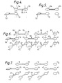
- FIG. 2a illustrates single lobe loop
- Fig. 2b illustrates a two lobe loop with the lobes 11 and 12 being of equal sizes.
- the circulation of a particular current through the loop of Fig. 2b generates a corresponding first magnetic flux value through the overall aperture of the circuit (loop).
- Magnetic flux is conserved within a superconducting loop, hence if more magnetic flux is added to that passing through lobe 11, say, in the direction into the paper as indicated by the two crosses (xx), there will result an equal and opposite magnetic flux in the overall circuit which is distributed within the circuit according to the inductance of each lobe.
- lobe structures and other multi-lobe structures enable coupling between various superconducting loops as will be apparent from the following.
- a superconducting flux transformer can be achieved by means of a superconducting circuit (loop) with two lobes 13, 14 of different inductances (Fig. 2c). This can be achieved by replacing one "circular" loop with a spiral, thus forming a two dimensional inductor, the interior area of the lobe 13 and the spiral being the same.
- a current circulating in the circuit of Fig. 2c generates a certain magnetic flux through the overall aperture of the loop.
- FIG. 3 A basic scheme for a successive approximation analogue to digital converter employing superconducting element is illustrated in Fig. 3. It comprises three layers.
- the top layer consists of an unbroken subtraction/addition superconducting circuit 30 with eight lobes 31, one lobe 31 for each bit of the ADC, an 8-bit ADC being illustrated, a sense loop 32 and a two-dimensional spiral inductor 33.
- the middle layer comprises a series of superconducting screening pads 34 a respective one aligned with each of the lobes 31.
- any of the pads 34 When a sufficiently large current is provided to any of the pads 34 it will be driven into a normal (non-superconducting) state and flux in a corresponding inductor 38 will be linked to the lobe 31 aligned therewith.
- the screening pads 34 are connected to a current switching network (not shown in Fig. 3) which can drive any permutation of the pads into the normal state, thus providing switchable barriers to magnetic flux.
- In the bottom layer loop 36 comprises a drive loop (non-superconducting) connected to a signal input indicated by 37. The drive loop 36 is aligned with sense loop 32.
- the inductors can be other than spiral, although the latter is currently preferred.
- the spiral reference inductors are connected to a current source 39.
- All of the conducting elements in the bottom layer are of non-superconducting material, such as copper.
- a magnetometer (comparator) 40 such as a Hall-effect device, which is aligned directly below the top layer inductor 33.
- a sample of an input analogue signal to be converted is taken at a predetermined time and applied to the drive loop 36.
- a sample and hold device may be employed, such will be unnecessary if the conversion takes place at a sufficiently rapid rate, particularly if the least significant digit does not change during the sampling time.
- a corresponding flux is produced in the spiral inductor 33 and detected by the comparator 40. Reference fluxes are then successively switched into the superconducting circuit 30 by applying current to or removing current from the various screening pads 34 until the net flux in the circuit 30, as measured by the comparator 40, is zero.
- the reference inductors 38 and source 39 constitute a reference flux store when current is flowing. Another form of a reference flux store which employs superconducting loops will be described in the following. This uses magnetic flux snares which will be described first.
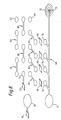
- Fig. 4 there is illustrated a two layer system including a loop 51 made of a normal conducting material (non-superconducting) such as copper wire, which is connected to a d.c. current source 52.
- the current source 52 supplies a current I1 which passes around the loop 51.
- the loop has self inductance L1.
- Reference numeral 53 indicates a superconducting flux transformer loop which has a lobe 54 at one end and a lobe 55 at the other end.
- the flux snare is comprised by a stand-alone superconducting loop aligned with lobe 55.
- FIG. 7 A three-layer system of flux transformers and flux snares based on those of Figs 4 and 5 can be used to produce a flux reference store, an example of which is illustrated in Fig. 7.
- Fig. 6 which indicates a somewhat similar arrangement will first be referred to.
- Reference numeral 51 again denotes a normal conducting loop and reference numeral 52 a d.c. current source.
- Reference numeral 53 again denotes a superconducting flux transformer loop with lobes 54 and 55 at its ends.
- Reference numerals 58, 59 and 60 denote similar superconducting flux transformer loops whose lobes are aligned in a network as indicated.
- Reference numerals 61, 62, 63 and 64 denote similar superconducting flux tranformer loops one lobe of each of which is aligned (as indicated by dashed lines) with two other loops/lobes so that there are triplets of loops/lobes linking flux.
- Reference numerals 57 and 65 denote snares comprising stand-alone superconducting loops. All of the lobes have identical inductance L which is equal to that of the snare loops. The connecting strips of the flux transformer loops are considered to have negligible inductance.
- current source 52 provides current in the normal loop 51 which generates a flux of +16 units therethrough.
- This flux is linked by transformers 53 and 61. These transformers must conserve flux and the only way they can do this is by generating -8 units of flux in each of their lobes. Thus there is no net flux in the loop 53/loop 51/loop 61 triplet. However, the -8 units at lobe 5 of transformer loop 53 are linked by tranformer loops 58 and 62. These two loops conserve flux by generating +4 units in each end lobe so that once again the net flux in the triplet is zero.
- the process continues down the line of triplets, terminating with transformer loop 60 and the two flux snares 57 and 65, which each generate -1/2 unit of flux.
- the flux transformers 61 to 64 are referred to as snare transformers. It should be noted that if these snare transformers were absent then the remaining loops would all contain either +16 or -16 units of flux.
- the snare transformers each contain half the flux quantity of the preceding one and the lobes of the snare transformers not in the triplets contain fluxes of -8, +4, -2, +1 units respectively.
- the polarities should all be the same. This can be achieved simply by arranging that the connecting strips of half of the snare transformers cross over, such as transformers 61 and 63 to achieve reference fluxes of +8, +4, +2, +1 units respectively as illustrated in Fig. 7, or alternatively (not shown) with transformers 62 and 64 crossed over, reference fluxes of -8, -4, -2, -1 units respectively.
- the flux reference store of Fig. 7 can be used as the basis of a magnetic flux analogue-to-digital converter as illustrated in Fig. 8.
- This is a five layer structure and includes in addition to the three layers of Figs 6 and 7, a layer including shields 66 and a layer including a collector (addition/subtraction) superconducting loop 68.
- the collector loop 68 has four lobes 74, one lobe 74 for each bit of the analogue-to-digital converter (ADC), a 4-bit ADC being illustrated, a sense loop 71 and a two-dimensional spiral inductor 72.
- a magnetometer (comparater) is required to be used as a null-field detector. This may be comprised by a Hall effect device 73 disposed within inductor 72.
- the inclusion of a spiral inductor 72 in loop 68 means that any flux linked by loop 68 will be concentrated at inductor 72.
- the shields 66 are superconducting screening pads which are each connected to a current source via a switching circuit (not shown). If the current source provides a sufficiently large current to a shield then it will be driven to a normal (non-superconducting) state and flux linked to one loop, say of snare transformer 61 will be passed through shield 66 and linked to corresponding lobe 74. Otherwise, when there is no current or it is too low, the shields 66 provide barriers to magnetic flux.
- Loop 69 is a non-superconducting drive loop which is connected to signal to be converted, which is indicated by a signal source 70.
- the drive loop 69 is aligned with the sense loop 71.
- Aligned with each of the lobes 74 of the collector loop 68 is a respective shield 66 and a respective lobe of one of the snare transformers 61 to 64 which is not in the triplet and which provides a reference flux value.
- a current is passed through the normal loop 51 corresponding to +16 units of flux and the flux reference store generates the reference values (+8,+4,+2,+1) at the lobes of snare transformers 61 to 64 not in the triplets, as described above.
- the shields 66 are all initially superconducting.
- the analogue signal to be converted is sampled and applied to the drive loop 69 and generates a corresponding magnetic flux passing therethrough, and the magnetic flux is linked to sense loop 71. Due to the spiral inductor 72 the magnetic flux linked to the collector loop 68 is concentrated at the spiral inductor and detected by the Hall-effect device 73.
- the reference fluxes are then successively switched in to the collector loop 68, by applying current to/removing current from the various shields 66, until the net flux in the collector loop 68, as measured by the Hall-effect device 73, is zero.
- the various superconducting and other structures refered to above are amenable to production in various ways.
- screen-printing, MOCVD, or sputtering with the various layers separated by insulating material, may be appropriate.
- Superconducting loops may be provided by such means or alternatively superconducting wire may be formed into the loops.
- the non-superconducting loops may be similarly formed.
- the newer superconducting materials with higher operating temperatures are employed.
- Possible superconducting materials which can be employed are niobium - niobium nitride (4.2K), YBa2 Cu3 0 7-x (95K) or thallium based compounds (125K ).
- the high speed, high accuracy analogue to digital converters provided by the present invention are particularly applicable to data acquisition systems, such as to the front ends of radars systems, for digital radio, or for other fast signal processing requirements.
Landscapes
- Engineering & Computer Science (AREA)
- Theoretical Computer Science (AREA)
- Analogue/Digital Conversion (AREA)
Applications Claiming Priority (4)
| Application Number | Priority Date | Filing Date | Title |
|---|---|---|---|
| GB8728497 | 1987-12-05 | ||
| GB878728497A GB8728497D0 (en) | 1987-12-05 | 1987-12-05 | A/d converters |
| GB8822360A GB2213334B (en) | 1987-12-05 | 1988-09-22 | Successive approximation a/d converters |
| GB8822360 | 1988-09-22 |
Publications (1)
| Publication Number | Publication Date |
|---|---|
| EP0320100A2 true EP0320100A2 (de) | 1989-06-14 |
Family
ID=26293164
Family Applications (1)
| Application Number | Title | Priority Date | Filing Date |
|---|---|---|---|
| EP88309780A Withdrawn EP0320100A2 (de) | 1987-12-05 | 1988-10-19 | Analogdigitalwandler |
Country Status (3)
| Country | Link |
|---|---|
| US (1) | US4940983A (de) |
| EP (1) | EP0320100A2 (de) |
| JP (1) | JPH01190127A (de) |
Cited By (2)
| Publication number | Priority date | Publication date | Assignee | Title |
|---|---|---|---|---|
| EP0414426A1 (de) * | 1989-08-24 | 1991-02-27 | Trw Inc. | Supraleitender Analog-zu-Digital-Konverter mit einem geerdeten Vier-Übergang-Squid-Zweirichtungszähler |
| EP0967488A2 (de) * | 1998-06-24 | 1999-12-29 | INSTITUT FÜR LUFT- UND KÄLTETECHNIK GEMEINNÜTZIGE GESELLSCHAFT mbH | Magnetometer |
Families Citing this family (9)
| Publication number | Priority date | Publication date | Assignee | Title |
|---|---|---|---|---|
| US5172019A (en) * | 1992-01-17 | 1992-12-15 | Burr-Brown Corporation | Bootstrapped FET sampling switch |
| US5272480A (en) * | 1992-08-17 | 1993-12-21 | Hewlett-Packard Company | Track and hold circuit with continuously suppressed Josephson effect |
| SE9600666L (sv) * | 1996-02-22 | 1997-08-23 | Pharmacia Biotech Ab | Detekteringsanordning |
| US6239596B1 (en) | 1997-06-09 | 2001-05-29 | Joseph J. Stupak, Jr. | Total magnetic flux measuring device |
| US6617926B2 (en) * | 2001-06-29 | 2003-09-09 | Intel Corporation | Tail current node equalization for a variable offset amplifier |
| US6608582B2 (en) * | 2001-06-29 | 2003-08-19 | Intel Corporation | A/D conversion using a variable offset comparator |
| US7026975B1 (en) * | 2004-03-29 | 2006-04-11 | Maxim Integrated Products, Inc. | High speed digital path for successive approximation analog-to-digital converters |
| GB0425800D0 (en) * | 2004-11-24 | 2004-12-22 | Koninkl Philips Electronics Nv | Montoring physical operating parameters of an integrated circuit |
| US8065022B2 (en) * | 2005-09-06 | 2011-11-22 | General Electric Company | Methods and systems for neural network modeling of turbine components |
Family Cites Families (15)
| Publication number | Priority date | Publication date | Assignee | Title |
|---|---|---|---|---|
| US2949602A (en) * | 1958-04-11 | 1960-08-16 | Ibm | Cryogenic converter |
| NL259295A (de) * | 1959-12-22 | 1900-01-01 | ||
| NL261458A (de) * | 1960-02-24 | |||
| US3259844A (en) * | 1961-10-26 | 1966-07-05 | Philips Corp | Signal amplitude discriminator having a plurality of superconducting loops arranged to respond to the magnetic field produced by the signal |
| US3983419A (en) * | 1974-12-31 | 1976-09-28 | International Business Machines - Ibm | Analog waveform transducing circuit |
| US4258354A (en) * | 1979-05-11 | 1981-03-24 | Amiram Carmon | Portable alarm device |
| US4315255A (en) * | 1980-10-27 | 1982-02-09 | The United States Of America As Represented By The Secretary Of The Navy | Multiple-quantum interference superconducting analog-to-digital converter |
| US4504153A (en) * | 1983-08-08 | 1985-03-12 | R. Dean Seeman | Pharmacist-programmable medication prompting system and method |
| US4551704A (en) * | 1983-09-27 | 1985-11-05 | International Business Machines Corporation | Look-back analog to digital converter |
| US4768177A (en) * | 1984-07-06 | 1988-08-30 | Kehr Bruce A | Method of and apparatus for alerting a patient to take medication |
| US4646060A (en) * | 1984-09-07 | 1987-02-24 | Trw Inc. | Superconducting analog-to-digital converter with bidirectional counter |
| US4695954A (en) * | 1984-10-31 | 1987-09-22 | Rose Robert J | Modular medication dispensing system and apparatus utilizing portable memory device |
| US4682299A (en) * | 1985-02-19 | 1987-07-21 | Kenneth B. McIntosh | Medication clock |
| US4672359A (en) * | 1985-11-12 | 1987-06-09 | Trw Inc. | Superconducting analog-to-digital converter and digital magnetometer and related method for its use |
| GB8728496D0 (en) * | 1987-12-05 | 1988-01-13 | Stc Plc | Superconductive devices |
-
1988
- 1988-10-19 EP EP88309780A patent/EP0320100A2/de not_active Withdrawn
- 1988-10-21 US US07/261,242 patent/US4940983A/en not_active Expired - Fee Related
- 1988-12-02 JP JP63305872A patent/JPH01190127A/ja active Pending
Cited By (3)
| Publication number | Priority date | Publication date | Assignee | Title |
|---|---|---|---|---|
| EP0414426A1 (de) * | 1989-08-24 | 1991-02-27 | Trw Inc. | Supraleitender Analog-zu-Digital-Konverter mit einem geerdeten Vier-Übergang-Squid-Zweirichtungszähler |
| EP0967488A2 (de) * | 1998-06-24 | 1999-12-29 | INSTITUT FÜR LUFT- UND KÄLTETECHNIK GEMEINNÜTZIGE GESELLSCHAFT mbH | Magnetometer |
| EP0967488A3 (de) * | 1998-06-24 | 2000-11-22 | INSTITUT FÜR LUFT- UND KÄLTETECHNIK GEMEINNÜTZIGE GESELLSCHAFT mbH | Magnetometer |
Also Published As
| Publication number | Publication date |
|---|---|
| JPH01190127A (ja) | 1989-07-31 |
| US4940983A (en) | 1990-07-10 |
Similar Documents
| Publication | Publication Date | Title |
|---|---|---|
| US4940983A (en) | A/D converters | |
| US5942997A (en) | Correlated superconductor single flux quantum analog-to-digital converter | |
| EP0222470B1 (de) | Supraleitender AD-Wandler und digitales Magnetometer und verwandtes Verfahren zu dessen Gebrauch | |
| US5162731A (en) | Superconducting quantum interference magnotometer having a feedback reset capability to extend the dynamic sensing range | |
| JP2000174612A (ja) | 超電導単一磁束量子論理回路 | |
| US4879488A (en) | Vernier for superconducting analog-to-digital converter | |
| EP0609916B1 (de) | Supraleitender Analog-Digitalwandler und Leseverfahren dafür | |
| US5872731A (en) | Multi-state Josephson memory | |
| US4977402A (en) | Nonhysteretic periodic-threshold SQUID comparator and A/D converter | |
| GB2213334A (en) | A/D converters | |
| US5351049A (en) | Superconducting quantizer and A/D converter system | |
| US5396242A (en) | Superconductivity binary odometer | |
| US5227755A (en) | Winding configuration for a cryomagnet | |
| US5012243A (en) | Superconducting analog-to-digital converter with floating four-junction squid bidirectional counter | |
| US5272480A (en) | Track and hold circuit with continuously suppressed Josephson effect | |
| JPS6079828A (ja) | アナログ−デイジタル変換装置 | |
| US4072940A (en) | Digital to analog resolver converter | |
| US6627894B2 (en) | Method for reading signals from plural elements simultaneously | |
| Radparvar et al. | An integrated digital SQUID magnetometer with high sensitivity input | |
| US5091728A (en) | D/A and A/D converters utilizing weighted impedances | |
| Lee et al. | Phase tree: a periodic, fractional flux quantum vernier for high-speed interpolation of analog-to-digital converters | |
| US3162775A (en) | Scanning device employing cryotron bridges connected in free-matrix for measuring magnitudes of selected input signals | |
| US5099238A (en) | Parallel analog to digital converter | |
| JP3645521B2 (ja) | 超電導体を用いたアナログ−デジタル変換器 | |
| Mallick | Computer simulations of a 20 gigasample/second, 500 MHz eight-bit, analog-to-digital converter |
Legal Events
| Date | Code | Title | Description |
|---|---|---|---|
| PUAI | Public reference made under article 153(3) epc to a published international application that has entered the european phase |
Free format text: ORIGINAL CODE: 0009012 |
|
| AK | Designated contracting states |
Kind code of ref document: A2 Designated state(s): DE FR IT |
|
| STAA | Information on the status of an ep patent application or granted ep patent |
Free format text: STATUS: THE APPLICATION IS DEEMED TO BE WITHDRAWN |
|
| 18D | Application deemed to be withdrawn |
Effective date: 19920504 |