EP0319000B1 - Ink jet head, substrate therefor, process for preparing thereof and ink jet apparatus having said head - Google Patents
Ink jet head, substrate therefor, process for preparing thereof and ink jet apparatus having said head Download PDFInfo
- Publication number
- EP0319000B1 EP0319000B1 EP88120088A EP88120088A EP0319000B1 EP 0319000 B1 EP0319000 B1 EP 0319000B1 EP 88120088 A EP88120088 A EP 88120088A EP 88120088 A EP88120088 A EP 88120088A EP 0319000 B1 EP0319000 B1 EP 0319000B1
- Authority
- EP
- European Patent Office
- Prior art keywords
- process according
- upper layer
- layer
- bias
- forming
- Prior art date
- Legal status (The legal status is an assumption and is not a legal conclusion. Google has not performed a legal analysis and makes no representation as to the accuracy of the status listed.)
- Expired - Lifetime
Links
- 239000000758 substrate Substances 0.000 title claims description 44
- 238000004519 manufacturing process Methods 0.000 title claims description 10
- 238000004544 sputter deposition Methods 0.000 claims description 45
- 238000000034 method Methods 0.000 claims description 30
- 239000007788 liquid Substances 0.000 claims description 23
- 230000008569 process Effects 0.000 claims description 19
- 238000000137 annealing Methods 0.000 claims description 11
- 238000007599 discharging Methods 0.000 claims description 8
- 230000008859 change Effects 0.000 claims description 3
- 239000011261 inert gas Substances 0.000 claims description 3
- 239000012298 atmosphere Substances 0.000 claims description 2
- 239000011347 resin Substances 0.000 claims description 2
- 229920005989 resin Polymers 0.000 claims description 2
- 239000010410 layer Substances 0.000 description 92
- 230000015572 biosynthetic process Effects 0.000 description 21
- 239000010408 film Substances 0.000 description 21
- 239000011241 protective layer Substances 0.000 description 15
- 230000007547 defect Effects 0.000 description 13
- VYPSYNLAJGMNEJ-UHFFFAOYSA-N Silicium dioxide Chemical compound O=[Si]=O VYPSYNLAJGMNEJ-UHFFFAOYSA-N 0.000 description 12
- 238000007641 inkjet printing Methods 0.000 description 11
- 229910052681 coesite Inorganic materials 0.000 description 6
- 229910052906 cristobalite Inorganic materials 0.000 description 6
- 230000008018 melting Effects 0.000 description 6
- 238000002844 melting Methods 0.000 description 6
- 239000002184 metal Substances 0.000 description 6
- 229910052751 metal Inorganic materials 0.000 description 6
- 239000000377 silicon dioxide Substances 0.000 description 6
- 235000012239 silicon dioxide Nutrition 0.000 description 6
- 229910052682 stishovite Inorganic materials 0.000 description 6
- 229910052905 tridymite Inorganic materials 0.000 description 6
- 230000008901 benefit Effects 0.000 description 5
- 230000006870 function Effects 0.000 description 5
- GWEVSGVZZGPLCZ-UHFFFAOYSA-N Titan oxide Chemical compound O=[Ti]=O GWEVSGVZZGPLCZ-UHFFFAOYSA-N 0.000 description 4
- 239000000463 material Substances 0.000 description 4
- 230000001681 protective effect Effects 0.000 description 4
- 230000006835 compression Effects 0.000 description 3
- 238000007906 compression Methods 0.000 description 3
- 238000005336 cracking Methods 0.000 description 3
- 238000000992 sputter etching Methods 0.000 description 3
- -1 Si3N4 Chemical class 0.000 description 2
- 230000001133 acceleration Effects 0.000 description 2
- 239000007789 gas Substances 0.000 description 2
- 238000002360 preparation method Methods 0.000 description 2
- 229910052715 tantalum Inorganic materials 0.000 description 2
- 239000010409 thin film Substances 0.000 description 2
- 230000007704 transition Effects 0.000 description 2
- 229910003862 HfB2 Inorganic materials 0.000 description 1
- 229910052581 Si3N4 Inorganic materials 0.000 description 1
- 230000009471 action Effects 0.000 description 1
- 239000000853 adhesive Substances 0.000 description 1
- 230000001070 adhesive effect Effects 0.000 description 1
- 230000005587 bubbling Effects 0.000 description 1
- 238000000576 coating method Methods 0.000 description 1
- 230000007797 corrosion Effects 0.000 description 1
- 238000005260 corrosion Methods 0.000 description 1
- 238000004925 denaturation Methods 0.000 description 1
- 230000036425 denaturation Effects 0.000 description 1
- 230000000694 effects Effects 0.000 description 1
- 239000007772 electrode material Substances 0.000 description 1
- 230000003028 elevating effect Effects 0.000 description 1
- 230000001747 exhibiting effect Effects 0.000 description 1
- 239000011521 glass Substances 0.000 description 1
- 238000010438 heat treatment Methods 0.000 description 1
- 230000006872 improvement Effects 0.000 description 1
- 239000011810 insulating material Substances 0.000 description 1
- 238000011835 investigation Methods 0.000 description 1
- 150000002500 ions Chemical class 0.000 description 1
- 229910044991 metal oxide Inorganic materials 0.000 description 1
- 150000004706 metal oxides Chemical class 0.000 description 1
- 229910052750 molybdenum Inorganic materials 0.000 description 1
- 150000004767 nitrides Chemical class 0.000 description 1
- 239000012299 nitrogen atmosphere Substances 0.000 description 1
- 230000003647 oxidation Effects 0.000 description 1
- 238000007254 oxidation reaction Methods 0.000 description 1
- 230000035515 penetration Effects 0.000 description 1
- 230000002265 prevention Effects 0.000 description 1
- 238000007639 printing Methods 0.000 description 1
- 230000009993 protective function Effects 0.000 description 1
- 230000009467 reduction Effects 0.000 description 1
- 230000002040 relaxant effect Effects 0.000 description 1
- 230000004044 response Effects 0.000 description 1
- 239000004065 semiconductor Substances 0.000 description 1
- XJKVPKYVPCWHFO-UHFFFAOYSA-N silicon;hydrate Chemical compound O.[Si] XJKVPKYVPCWHFO-UHFFFAOYSA-N 0.000 description 1
- PBCFLUZVCVVTBY-UHFFFAOYSA-N tantalum pentoxide Inorganic materials O=[Ta](=O)O[Ta](=O)=O PBCFLUZVCVVTBY-UHFFFAOYSA-N 0.000 description 1
- 230000002463 transducing effect Effects 0.000 description 1
- 229910052721 tungsten Inorganic materials 0.000 description 1
- ZNOKGRXACCSDPY-UHFFFAOYSA-N tungsten(VI) oxide Inorganic materials O=[W](=O)=O ZNOKGRXACCSDPY-UHFFFAOYSA-N 0.000 description 1
- 238000007740 vapor deposition Methods 0.000 description 1
Images

Classifications
-
- B—PERFORMING OPERATIONS; TRANSPORTING
- B41—PRINTING; LINING MACHINES; TYPEWRITERS; STAMPS
- B41J—TYPEWRITERS; SELECTIVE PRINTING MECHANISMS, i.e. MECHANISMS PRINTING OTHERWISE THAN FROM A FORME; CORRECTION OF TYPOGRAPHICAL ERRORS
- B41J2/00—Typewriters or selective printing mechanisms characterised by the printing or marking process for which they are designed
- B41J2/005—Typewriters or selective printing mechanisms characterised by the printing or marking process for which they are designed characterised by bringing liquid or particles selectively into contact with a printing material
- B41J2/01—Ink jet
- B41J2/135—Nozzles
- B41J2/16—Production of nozzles
- B41J2/1621—Manufacturing processes
- B41J2/164—Manufacturing processes thin film formation
- B41J2/1642—Manufacturing processes thin film formation thin film formation by CVD [chemical vapor deposition]
-
- B—PERFORMING OPERATIONS; TRANSPORTING
- B41—PRINTING; LINING MACHINES; TYPEWRITERS; STAMPS
- B41J—TYPEWRITERS; SELECTIVE PRINTING MECHANISMS, i.e. MECHANISMS PRINTING OTHERWISE THAN FROM A FORME; CORRECTION OF TYPOGRAPHICAL ERRORS
- B41J2/00—Typewriters or selective printing mechanisms characterised by the printing or marking process for which they are designed
- B41J2/005—Typewriters or selective printing mechanisms characterised by the printing or marking process for which they are designed characterised by bringing liquid or particles selectively into contact with a printing material
- B41J2/01—Ink jet
- B41J2/135—Nozzles
- B41J2/14—Structure thereof only for on-demand ink jet heads
- B41J2/14016—Structure of bubble jet print heads
- B41J2/14088—Structure of heating means
- B41J2/14112—Resistive element
- B41J2/14129—Layer structure
-
- B—PERFORMING OPERATIONS; TRANSPORTING
- B41—PRINTING; LINING MACHINES; TYPEWRITERS; STAMPS
- B41J—TYPEWRITERS; SELECTIVE PRINTING MECHANISMS, i.e. MECHANISMS PRINTING OTHERWISE THAN FROM A FORME; CORRECTION OF TYPOGRAPHICAL ERRORS
- B41J2/00—Typewriters or selective printing mechanisms characterised by the printing or marking process for which they are designed
- B41J2/005—Typewriters or selective printing mechanisms characterised by the printing or marking process for which they are designed characterised by bringing liquid or particles selectively into contact with a printing material
- B41J2/01—Ink jet
- B41J2/135—Nozzles
- B41J2/16—Production of nozzles
- B41J2/1601—Production of bubble jet print heads
- B41J2/1604—Production of bubble jet print heads of the edge shooter type
-
- B—PERFORMING OPERATIONS; TRANSPORTING
- B41—PRINTING; LINING MACHINES; TYPEWRITERS; STAMPS
- B41J—TYPEWRITERS; SELECTIVE PRINTING MECHANISMS, i.e. MECHANISMS PRINTING OTHERWISE THAN FROM A FORME; CORRECTION OF TYPOGRAPHICAL ERRORS
- B41J2/00—Typewriters or selective printing mechanisms characterised by the printing or marking process for which they are designed
- B41J2/005—Typewriters or selective printing mechanisms characterised by the printing or marking process for which they are designed characterised by bringing liquid or particles selectively into contact with a printing material
- B41J2/01—Ink jet
- B41J2/135—Nozzles
- B41J2/16—Production of nozzles
- B41J2/1621—Manufacturing processes
- B41J2/1631—Manufacturing processes photolithography
-
- B—PERFORMING OPERATIONS; TRANSPORTING
- B41—PRINTING; LINING MACHINES; TYPEWRITERS; STAMPS
- B41J—TYPEWRITERS; SELECTIVE PRINTING MECHANISMS, i.e. MECHANISMS PRINTING OTHERWISE THAN FROM A FORME; CORRECTION OF TYPOGRAPHICAL ERRORS
- B41J2/00—Typewriters or selective printing mechanisms characterised by the printing or marking process for which they are designed
- B41J2/005—Typewriters or selective printing mechanisms characterised by the printing or marking process for which they are designed characterised by bringing liquid or particles selectively into contact with a printing material
- B41J2/01—Ink jet
- B41J2/135—Nozzles
- B41J2/16—Production of nozzles
- B41J2/1621—Manufacturing processes
- B41J2/164—Manufacturing processes thin film formation
- B41J2/1646—Manufacturing processes thin film formation thin film formation by sputtering
-
- B—PERFORMING OPERATIONS; TRANSPORTING
- B41—PRINTING; LINING MACHINES; TYPEWRITERS; STAMPS
- B41J—TYPEWRITERS; SELECTIVE PRINTING MECHANISMS, i.e. MECHANISMS PRINTING OTHERWISE THAN FROM A FORME; CORRECTION OF TYPOGRAPHICAL ERRORS
- B41J2202/00—Embodiments of or processes related to ink-jet or thermal heads
- B41J2202/01—Embodiments of or processes related to ink-jet heads
- B41J2202/03—Specific materials used
Definitions
- This invention relates to an ink jet head to be used in an ink jet recording apparatus which performs recording by forming droplets of ink by discharging ink and attaching the droplets onto a recording medium such as paper, etc., a substrate for the head, processes for preparing thereof and an ink jet apparatus having the head.
- the ink jet recording method is a recording method which performs recording by discharging ink (recording liquid) from a discharge opening provided at the ink jet recording head and attaching the ink onto a recording medium such as paper, etc., which has many advantages that it is extremely small in generation of noise, and capable of high speed recording, and yet recording can be practiced on plain paper, etc. without use of a special recording paper, and various typed of recording heads have been developed.
- the recording head of the type which discharges ink from a discharge opening by permitting heat energy to act on ink as disclosed in Japanese Laid-open Patent Application No. 54-59936, German Laid-open Patent Application (DOLS) No. 2843064 and U.S. Patent 4723129 has such advantages as good response to recording signals, easy multi-formation of discharge openings, etc.
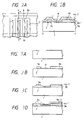
- FIGs. 1A and 1B Representative constitutions of such a recording head of the type utilizing heat energy as the ink discharging energy are shown in Figs. 1A and 1B.
- the recording head has a constitution formed by bonding a substrate comprising an electrothermal transducer provided for transducing electrical energy to heat energy utilized for ink discharging arranged on the surface exhibiting insulating property of the support 1, and further, if necessary, an upper layer 4 as the protective layer provided at least on the heat-generating resistor 8 and the electrodes 3 of the electrothermal transducer to be finally positioned below the liquid path 6 and the liquid chamber 10 communicated with the ink supplying inlet 9 to a covering member 5 having a recessed portion for forming the liquid path 6 and the liquid chamber 10, etc. formed thereon, such a recording head being disclosed e.g. in DE-A-3416059.
- the energy to be utilized for discharging ink in this recording head is imparted by an electrothermal transducer having a pair of electrodes 3 and a heat-generating resistor 8 positioned between the pair of electrodes. That is, when current is applied on the electrodes 3 to generate heat from the heat-generating resistor, the ink in the liquid path 6 near the heat-generating portion 8 is momentarily heated to generate bubbles thereat, and through volume change by momentary volume expansion and shrinkage by generation of the bubbles, a droplet of ink is discharged.
- the upper layer as the protective layer to be provided on the heat generating resistor and electrodes of the substrate in the constitution of the recording head as described above is provided for the purpose of preventing galvanic corrosion or electrical dielectric failure at the heat generating resistor or electrodes by contact with ink or penetration of ink, and it must be free from defect and good in step coverage.
- Japanese Laid-open Patent Application No. 60-234850 discloses a constitution using a layer formed by the bias sputtering method for the upper layer.
- the defects become reduced, step coverage becomes better, and durability is improved. Also, as compared with the sputtering method, the defects can be reduced even with the same thickness, and therefore the film thickness can be made thinner. Accordingly, improvement of characteristics and cost down can be effected.
- bias sputtered layer a layer formed by the bias sputtering method
- the protective films made to have a multi-layer constitution in order to give functionally more characteristics as disclosed
- An Japanese Laid-open Patent Application No. 59-194866 there ensued the problem that a protective film of good protective function cannot necessarily be obtained.
- An object of the present invention is to enable effective application of a bias sputtered layer to the protective layer.
- Another object of the present invention is to provide an ink jet head provided with a protective layer having a bias sputtered layer, having high reliability and excellent durability, a substrate for the head, processes for preparing thereof and an ink jet apparatus provided with the head.
- a process for preparing an ink jet head having a support, an electrothermal transducer provided on the support and having a heat-generating resistor and a pair of electrodes electrically connected to the heat-generating resistor, a first upper layer provided on the electrothermal transducer, a second upper layer provided on the first upper layer and a liquid path communicated with a discharge opening for discharging liquid and formed on the support so as to correspond to the heat-generating portion of the electrothermal transducer formed between the pair of electrodes, which comprises the steps of: forming the first upper layer by the bias sputtering method at the absolute value of the bias voltage of 50V or less and forming the second upper layer by the bias sputtering method at the absolute value of the bias voltage of 70V or higher.
- a process for preparing a substrate for ink jet heads having a support, an electrothermal transducer provided on the support and having a heat-generating resistor and a pair of electrodes electrically connected to the heat-generating resistor, a first upper layer provided on the electrothermal transducer and a second upper layer provided on the first upper layer, which comprises the steps of: forming the first upper layer by the bias sputtering method at the absolute value of the bias voltage of 50V or less and forming the second upper layer by the bias sputtering method at the absolute value of the bias voltage of 70V or higher.
- Fig. 1A is a schematic partial sectional view taken along the liquid path in an example of an ink jet head.
- Fig. 1B is a schematic perspective view showing the appearance of an example of an ink jet head in a separated state.
- Fig. 2A is a schematic plan view for illustrating the principal portion of an example of the ink jet head in accordance with the present invention.
- Fig. 2B is a schematic sectional view taken along the line X - Y in Fig. 2A for illustrating the principal portion of this example of the ink jet head in accordance with the present invention.
- Figs. 3A - 3D are each schematic sectional views for showing the preparation steps of the ink jet head in accordance with the present invention shown in Figs. 2A and 2B.
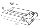
- Fig. 4 is a schematic perspective view of the ink jet apparatus provided with the ink jet head in accordance with the present invention.
- the present inventors have analyzed and investigated about the cause for such defects, and consequently found that the frequency of occurrence of the defect as described above depends on the operation conditions of bias sputtering, particularly the bias voltage to obtain the conclusion that an ink jet recording head and a substrate to be used for preparation thereof of good quality can be prepared by layer formation according to the bias sputtering method in which different bias sputtering steps with the respective specified operational conditions are used, thus accomplishing the present invention.
- the bias sputtering method is a method in which the base plate for film formation is lowered in potential than GND simultaneously with lowering the target side in potential than GND (sputtering method). More specifically, simultaneously with sputtering of, for example, Ar ions (Ar+) on the target side, the side of the base plate for film formation is also sputtered (sputter etching).
- the heat-generating resistor layer is formed as a very thin film in many cases, and when the heat-generating resistor layer is locally sputter etched to cause reduction in film thickness at that portion, no film thickness as designed will be consequently obtained in the heat-generating resistor and the recording head by use of the substrate thus prepared is liable to cause local power concentration in the heat-generating resistor during driving, thereby causing lowering in durability.
- the bias voltage is required to be set higher, and if the bias voltage is made lower, there sometimes ensues the problem particularly in the step coverage itself of the upper layer.
- the present inventors have analyzed the relationship between such bias voltage and the quality of the substrate for recording head, and consequently found that the problems as described above can be cancelled by forming the bias sputtered layer under the operational conditions in which specific different bias sputtering steps are combined.
- a bias sputtered layer by use of a low bias voltage is formed, and then on the bias sputtered layer thus formed, a bias sputtered layer by use of a high bias voltage necessary primarily for obtaining good step coverage is laminated.
- the voltage to be used in the first bias sputtering step by use of a low bias voltage may be desirably 50 V or lower, preferably 20 V or lower in terms of absolute value, while the voltage to be used in the second sputtering step by use of a high bias voltage is 70 V or higher, preferably 100 V or higher in terms of absolute value.
- an upper layer having good step coverage and adhesion as well as good function can be formed without affecting deleteriously the electrothermal transducer on the substrate.
- the bias voltage is sufficiently low and therefore no damage will be given to the electrothermal transducer on the substrate at all.
- the substrate surface having the electrothermal transducer provided thereon is protected from sputter etching with the layer formed in the first sputtering step, and therefore film formation can be practiced at a high bias voltage necessary for obtaining a protective film having the desired function.
- bias sputtered layer having good step coverage and good function can be obtained. Moreover, the bias sputtered layer is also excellent in adhesion to the support side.
- the bias sputtering step may be practiced in two divided steps as described above, or it may be also divided into 3 steps or more, but even in such case, a bias sputtering step of a low voltage (50 V or lower in terms of absolute value) is used for formation of the layer constituting the contact surface with the support side.
- a bias sputtering step of a low voltage 50 V or lower in terms of absolute value
- the problem of peel-off of the protective layer due to generation of cracks particularly at the step portion of, for example, a protective layer of multi layer structure having a bias sputtered layer and a layer comprising a high melting metal provided on the bias sputtered layer may be considered to be caused by the residual strain primarily within the bias sputtered layer, and such problem can be cancelled by relaxing the residual stress.
- the thin film comprising a high melting metal has great compression stress, and when a high melting metal is laminated on the bias sputtered layer, the compression stress of the high melting metal will act so as to increase the compression stress of the bias sputtered layer itself, where by generation of such a defect will become more marked.
- the problem regarding reliability in step stress test, etc. may be considered to be caused by the extent of the residual stress in the bias sputtered layer itself.
- the step stress test is an acceleration test of heat cycle, and lowering in reliability in the test is caused primarily by peeling or cracking already occurred in the protective layer, or peeling or cracking which is generated or progressed during the test. Accordingly, it may be considered that peeling or cracking portion has been already formed during formation of the bias sputtered layer, or the layer is under the state susceptible to occurrence of these defects and that causes of these defects are related to the residual stress of the layer.
- the layer is subjected to annealing treatment to remove the residual stress in the bias sputtered layer, whereby the above problem is cancelled.
- At least one layer constituting the protective layer is formed by using a material, for example, a metal oxide such as SiO2, TiO2, WO3, Ta2O5 and others, a highly resistant nitride such as Si3N4, AlN, etc. and other highly resistant semiconductors, etc.
- a material for example, a metal oxide such as SiO2, TiO2, WO3, Ta2O5 and others, a highly resistant nitride such as Si3N4, AlN, etc. and other highly resistant semiconductors, etc.
- the annealing treatment which is carried out after layer formation according to the bias sputtering method may be practiced by selecting suitably the heating conditions necessary for reducing effectively the residual stress in the bias sputtered layer as described above depending on the kind of the bias sputtered layer to be annealed or the operational conditions of the bias sputtering method used for its formation.
- the temperature condition 300 °C or higher is desirable, preferably 400 °C or higher.
- the upper limit may be the temperature which the electrode material can stand.
- a substrate for ink jet recording head having the constitution as shown in Figs. 2A and 2B was prepared as described below.
- Al was vapor deposited to a film thickness of 0.6 »m as the electrode layer 3, and further these layers were patterned by use of the photolithographic technique to form an electrothermal transducer having a heat-generating portion 8 provided between a pair at electrodes 3a and 3b (see Fig. 3B).
- a layer 4a-1 (film thickness 1 »m) comprising SiO2 was laminated according to the bias sputtering method under the following conditions (see Fig. 4C).
- Sputtering power 7.6 W/cm2 Bias voltage: -20 V
- Sputtering gas species Ar Sputtering gas pressure: 5 x 10 ⁇ 1 Pa
- Substrate-target interval 80 mm
- a layer 4a-2 (film thickness 0.9 »m) comprising SiO2 was laminated on the layer 4a - 1 by the bias sputtering method under the same conditions as described above except for changing the bias voltage to -150 V (see Fig. 3D).
- a layer 4b (film thickness 0.6 »m) comprising Ta was laminated by sputtering to obtain a support for ink jet recording heads (see Fig. 2B).
- substrates for ink jet recording heads were obtained in the same manner as described above except for changing both of the bias voltages during formation of the layers 4a-1, 4a-2 to -150 V.
- the value M determined from this formula indicates reliability of the electrothermal transducer of the substrate, representing the value used as the acceleration test of reliability in the product form, and the product is not so practically applicable if this value is 1.3 or lower.
- Table 1 Sample No. 1st -20V 2nd -150V only -150 V 4 1.65 1.33 12 1.63 1.29 17 1.67 1.35
- defects of the upper layer such as peeling or crack were generated at extremely low ratio in the substrates prepared according to the present invention, and also step coverage thereof was good.
- a substrate for ink jetting in accordance with the present invention was prepared in the same manner as in Example 1 with the exception that the bias voltage was not changed rapidly within a short time but changed gradually and continuously from -20V to -150V in transition from the step of Fig. 3C to the step of Fig. 3D.
- a substrate for ink jetting in accordance with the present invention was prepared in the same manner as in Example 1 with the exception that the layer 4b shown in Fig. 2B was not formed.
- a substrate for ink jetting in accordance with the present invention was prepared in the same menner as in Example 2 with the exception that the layer 4b shown in Fig. 3B was not formed.
- a substrate for ink jetting in accordance with the present invention was prepared in the same manner as in Example 1 except for using TiO2 in place of SiO2 as the material of the layer 4a - 1.
- a substrate for ink jetting in accordance with the present invention was prepared in the same manner as in Example 1 with the exception that after the step of Fig. 3C, the layer 4a - 1 is subjected to annealing treatment at 400°C under nitrogen atmosphere for 60 minutes in advance of the step of Fig. 3D.
- the bias voltage need not necessarily be changed rapidly (in Example 1, changed from -20V to -150V) and may be changed gradually and continuously.
- Example 1 As a typical example, better effects can be obtained by subjecting the bias sputtered layer to annealing treatment.
- the layer other than the bias sputtered layer to be used for the protective layer in the present invention it is possible to utilize one conventionally used for the protective layer of the substrates for recording heads such as those which can be formed into film by various film formation methods such as vapor deposition method, the sputtering method, etc. by use of a material such as a high melting metal, for example, Ta, W, Mo, etc., or organic coatings such as polymide, polyiamide, polyimideamide, cyclized rubber, etc.
- a material such as a high melting metal, for example, Ta, W, Mo, etc.
- organic coatings such as polymide, polyiamide, polyimideamide, cyclized rubber, etc.
- the substrates obtained by use of the method of the present invention in Examples were bonded to a covering member 5 made of glass and having a recessed portion for forming a liquid path 6, a liquid chamber 10, etc. to prepared ink jet recording heads.
- the substrate for ink jetting prepared in accordance with the present invention is utilized to prepare an ink jet head, specifically where the path having the liquid path 6 and the liquid chamber 10 as shown in Fig. 1 is to be formed, it is possible to form the wall of the path by using, for example, a photosensitive resin and then to bond the top plate to the member for forming the wall.
- the method of the present invention is applicable to an ink jet recording head and a substrate to be used for forming the head of any constitution comprising an upper layer as the protective film having a layer formed by the bias sputtering method as a part of its constitution.
- the present invention is not limited to this type and is applicable to heads of the type where the above two directions are different from each other (e.g. those where the two directions are perpendicular to each other).
- the layer of heat generating resistor and the layer of electrodes may be provided in a reverse (upset) arrangement.
- Fig. 4 is a schematic perspective view showing the appearance of a liquid jet apparatus equipped with the liquid jet head of the present invention.
- 1000 is the apparatus body, 1100 a power switch, 1200 an operation panel.
- the electrothermal transducer provided on the support is protected through the action of the layer bias sputtered at low voltage previously formed, thereby excluding the bad influence by bias sputtering, and yet by further addition of the bias sputtered layer at high voltage, and a process for preparing a substrate to be used for formation of the head an ink jet recording head provided with a protective layer having excellent coverage and adhesion as well as good function can be provided.
- the residual stress of the bias sputtered layer which can become the cause for giving rise to the defect of protecive layer can be effectively reduced by the annealing treatment, whereby there can be provided a process for preparing an ink jet recording head having excellent reliability and durability which utilizes fully the advantage of using the bias sputtering method and a process for preparing a substrate to be used for formation of the head.
- the residual stress of the bias sputtered layer which can become a cause to give rise to the defect of protective layer is controlled to be effectively reduced by its formation conditions, it becomes possible to provide a process for preparing an ink jet recording head having excellent reliability, durability and quality which has utilized fully the advantage of using the bias sputtering method and a process for preparing a substrate to be used for formation of the head.
Description
- This invention relates to an ink jet head to be used in an ink jet recording apparatus which performs recording by forming droplets of ink by discharging ink and attaching the droplets onto a recording medium such as paper, etc., a substrate for the head, processes for preparing thereof and an ink jet apparatus having the head.
- The ink jet recording method is a recording method which performs recording by discharging ink (recording liquid) from a discharge opening provided at the ink jet recording head and attaching the ink onto a recording medium such as paper, etc., which has many advantages that it is extremely small in generation of noise, and capable of high speed recording, and yet recording can be practiced on plain paper, etc. without use of a special recording paper, and various typed of recording heads have been developed.
- Among them, the recording head of the type which discharges ink from a discharge opening by permitting heat energy to act on ink as disclosed in Japanese Laid-open Patent Application No. 54-59936, German Laid-open Patent Application (DOLS) No. 2843064 and U.S. Patent 4723129 has such advantages as good response to recording signals, easy multi-formation of discharge openings, etc.
- Representative constitutions of such a recording head of the type utilizing heat energy as the ink discharging energy are shown in Figs. 1A and 1B.
- The recording head has a constitution formed by bonding a substrate comprising an electrothermal transducer provided for transducing electrical energy to heat energy utilized for ink discharging arranged on the surface exhibiting insulating property of the
support 1, and further, if necessary, an upper layer 4 as the protective layer provided at least on the heat-generatingresistor 8 and theelectrodes 3 of the electrothermal transducer to be finally positioned below the liquid path 6 and theliquid chamber 10 communicated with the ink supplying inlet 9 to a covering member 5 having a recessed portion for forming the liquid path 6 and theliquid chamber 10, etc. formed thereon, such a recording head being disclosed e.g. in DE-A-3416059. - The energy to be utilized for discharging ink in this recording head is imparted by an electrothermal transducer having a pair of
electrodes 3 and a heat-generatingresistor 8 positioned between the pair of electrodes. That is, when current is applied on theelectrodes 3 to generate heat from the heat-generating resistor, the ink in the liquid path 6 near the heat-generatingportion 8 is momentarily heated to generate bubbles thereat, and through volume change by momentary volume expansion and shrinkage by generation of the bubbles, a droplet of ink is discharged. - The upper layer as the protective layer to be provided on the heat generating resistor and electrodes of the substrate in the constitution of the recording head as described above is provided for the purpose of preventing galvanic corrosion or electrical dielectric failure at the heat generating resistor or electrodes by contact with ink or penetration of ink, and it must be free from defect and good in step coverage.
- From such standpoint, various investigations have been made about the materials for constituting the upper layer and the methods for formation thereof.
- For example, Japanese Laid-open Patent Application No. 60-234850 discloses a constitution using a layer formed by the bias sputtering method for the upper layer.
- By forming thus the upper layer according to the bias sputtering method, defects become reduced, step coverage becomes better, and durability is improved. Also, as compared with the sputtering method, the defects can be reduced even with the same thickness, and therefore the film thickness can be made thinner. Accordingly, improvement of characteristics and cost down can be effected.
- Whereas, in formation of the upper layer according to the bias sputtering method, there still remain problems to be solved. For example, in the recording head prepared by use of a substrate provided with an upper layer having a bias sputtered layer, defects such as poor printing or lowering in durability are liable to occur.
- Whereas, when a layer formed by the bias sputtering method (bias sputtered layer) is used for at least one layer of the protective films made to have a multi-layer constitution in order to give functionally more characteristics as disclosed An Japanese Laid-open Patent Application No. 59-194866, there ensued the problem that a protective film of good protective function cannot necessarily be obtained.
- For example, when an inorganic insulating material layer such as SiO₂ is formed by the bias sputtering method, and further a high melting metal such as Ta is laminated thereon according to the sputtering method, cracks are remarkably generated particularly at the step portion (step difference portion in patterns of layer of electrodes), and peel-off of the protective layer is liable to occur at that portion, and also in the recording head prepared by use of a substrate having such constitution, breaking of electodes and heat-generating resistors at low voltage may occur, whereby reliability is inferior and also durability in durability test such as step stress test may be low.
- Thus, when a bias sputtered layer is used as the protective layer, particularly when it is made a multi-layer constitution, not only the advantage of using the bias sputtered layer cannot be fully utilized, but also there is a problem that no protective layer of good quality can be formed.
- An object of the present invention is to enable effective application of a bias sputtered layer to the protective layer.
- Another object of the present invention is to provide an ink jet head provided with a protective layer having a bias sputtered layer, having high reliability and excellent durability, a substrate for the head, processes for preparing thereof and an ink jet apparatus provided with the head.
- According to the first aspect of the present invention, there is provided a process for preparing an ink jet head having a support, an electrothermal transducer provided on the support and having a heat-generating resistor and a pair of electrodes electrically connected to the heat-generating resistor, a first upper layer provided on the electrothermal transducer, a second upper layer provided on the first upper layer and a liquid path communicated with a discharge opening for discharging liquid and formed on the support so as to correspond to the heat-generating portion of the electrothermal transducer formed between the pair of electrodes, which comprises the steps of:
forming the first upper layer by the bias sputtering method at the absolute value of the bias voltage of 50V or less and
forming the second upper layer by the bias sputtering method at the absolute value of the bias voltage of 70V or higher. - According to the second aspect of the present invention, there is provided a process for preparing a substrate for ink jet heads having a support, an electrothermal transducer provided on the support and having a heat-generating resistor and a pair of electrodes electrically connected to the heat-generating resistor, a first upper layer provided on the electrothermal transducer and a second upper layer provided on the first upper layer, which comprises the steps of:
forming the first upper layer by the bias sputtering method at the absolute value of the bias voltage of 50V or less and
forming the second upper layer by the bias sputtering method at the absolute value of the bias voltage of 70V or higher. - Fig. 1A is a schematic partial sectional view taken along the liquid path in an example of an ink jet head.
- Fig. 1B is a schematic perspective view showing the appearance of an example of an ink jet head in a separated state.
- Fig. 2A is a schematic plan view for illustrating the principal portion of an example of the ink jet head in accordance with the present invention.
- Fig. 2B is a schematic sectional view taken along the line X - Y in Fig. 2A for illustrating the principal portion of this example of the ink jet head in accordance with the present invention.
- Figs. 3A - 3D are each schematic sectional views for showing the preparation steps of the ink jet head in accordance with the present invention shown in Figs. 2A and 2B.
- Fig. 4 is a schematic perspective view of the ink jet apparatus provided with the ink jet head in accordance with the present invention.
- The present invention had been accomplished on the basis of the findings by the present inventors as described below.
- That is, the present inventors have analyzed and investigated about the cause for such defects, and consequently found that the frequency of occurrence of the defect as described above depends on the operation conditions of bias sputtering, particularly the bias voltage to obtain the conclusion that an ink jet recording head and a substrate to be used for preparation thereof of good quality can be prepared by layer formation according to the bias sputtering method in which different bias sputtering steps with the respective specified operational conditions are used, thus accomplishing the present invention.
- The bias sputtering method is a method in which the base plate for film formation is lowered in potential than GND simultaneously with lowering the target side in potential than GND (sputtering method). More specifically, simultaneously with sputtering of, for example, Ar ions (Ar⁺) on the target side, the side of the base plate for film formation is also sputtered (sputter etching).
- Whereas, in film formation according to the bias sputtering method, since the base plate for film formation is subjected to sputter etching, if film formation is performed by use of a base plate for film formation having an electrothermal transducer formed on a support as shown in Fig. 1, there are times when damages are given to the electrothermal transducer on the support.
- Particularly, the heat-generating resistor layer is formed as a very thin film in many cases, and when the heat-generating resistor layer is locally sputter etched to cause reduction in film thickness at that portion, no film thickness as designed will be consequently obtained in the heat-generating resistor and the recording head by use of the substrate thus prepared is liable to cause local power concentration in the heat-generating resistor during driving, thereby causing lowering in durability.
- Such defects will become more marked as the bias voltage is higher.
- However, for obtaining an upper layer having good step coverage as well as excellent functions, the bias voltage is required to be set higher, and if the bias voltage is made lower, there sometimes ensues the problem particularly in the step coverage itself of the upper layer.
- The present inventors have analyzed the relationship between such bias voltage and the quality of the substrate for recording head, and consequently found that the problems as described above can be cancelled by forming the bias sputtered layer under the operational conditions in which specific different bias sputtering steps are combined.
- More specifically, in the method of the present invention, on the surface of the substrate on which an electrothermal transducer is provided, a bias sputtered layer by use of a low bias voltage is formed, and then on the bias sputtered layer thus formed, a bias sputtered layer by use of a high bias voltage necessary primarily for obtaining good step coverage is laminated.
- The voltage to be used in the first bias sputtering step by use of a low bias voltage may be desirably 50 V or lower, preferably 20 V or lower in terms of absolute value, while the voltage to be used in the second sputtering step by use of a high bias voltage is 70 V or higher, preferably 100 V or higher in terms of absolute value.
- By such bias sputtering process divided into at least 2 steps, an upper layer having good step coverage and adhesion as well as good function can be formed without affecting deleteriously the electrothermal transducer on the substrate. More specifically, in the first bias sputtering step of a low voltage, the bias voltage is sufficiently low and therefore no damage will be given to the electrothermal transducer on the substrate at all. Further, in the second bias sputtering step, the substrate surface having the electrothermal transducer provided thereon is protected from sputter etching with the layer formed in the first sputtering step, and therefore film formation can be practiced at a high bias voltage necessary for obtaining a protective film having the desired function.
- As the result, a bias sputtered layer having good step coverage and good function can be obtained. Moreover, the bias sputtered layer is also excellent in adhesion to the support side.
- In forming the bias sputtered layer, the bias sputtering step may be practiced in two divided steps as described above, or it may be also divided into 3 steps or more, but even in such case, a bias sputtering step of a low voltage (50 V or lower in terms of absolute value) is used for formation of the layer constituting the contact surface with the support side.
The problem of peel-off of the protective layer due to generation of cracks particularly at the step portion of, for example, a protective layer of multi layer structure having a bias sputtered layer and a layer comprising a high melting metal provided on the bias sputtered layer may be considered to be caused by the residual strain primarily within the bias sputtered layer, and such problem can be cancelled by relaxing the residual stress. - In other words, if the residual stress in the bias sputtered layer is high, this will act on the step portion which is structurally weak in adhesive force to give rise to cracks there, which may become the cause for peel-off. Besides, the thin film comprising a high melting metal has great compression stress, and when a high melting metal is laminated on the bias sputtered layer, the compression stress of the high melting metal will act so as to increase the compression stress of the bias sputtered layer itself, where by generation of such a defect will become more marked.
- On the other hand, the problem regarding reliability in step stress test, etc. may be considered to be caused by the extent of the residual stress in the bias sputtered layer itself. More specifically, the step stress test is an acceleration test of heat cycle, and lowering in reliability in the test is caused primarily by peeling or cracking already occurred in the protective layer, or peeling or cracking which is generated or progressed during the test. Accordingly, it may be considered that peeling or cracking portion has been already formed during formation of the bias sputtered layer, or the layer is under the state susceptible to occurrence of these defects and that causes of these defects are related to the residual stress of the layer.
- Therefore, by making the residual stress in the bias sputtered layer sufficiently small, these problems can be solved.
- In the method of the present invention, after formation of a layer according to the bias sputtering method, the layer is subjected to annealing treatment to remove the residual stress in the bias sputtered layer, whereby the above problem is cancelled.
- In the present invention, by use of the bias sputtering method as described above, at least one layer constituting the protective layer is formed by using a material, for example, a metal oxide such as SiO₂, TiO₂, WO₃, Ta₂O₅ and others, a highly resistant nitride such as Si₃N₄, AℓN, etc. and other highly resistant semiconductors, etc.
- The annealing treatment which is carried out after layer formation according to the bias sputtering method may be practiced by selecting suitably the heating conditions necessary for reducing effectively the residual stress in the bias sputtered layer as described above depending on the kind of the bias sputtered layer to be annealed or the operational conditions of the bias sputtering method used for its formation.
- As the temperature condition, 300 °C or higher is desirable, preferably 400 °C or higher. The upper limit may be the temperature which the electrode material can stand.
- In carrying out the annealing treatment, for prevention of thermal denaturation, etc., it is deairably conducted under an inert gas atmosphere such as N₂.
- The present invention is described in more detail by referring to Examples.
- A substrate for ink jet recording head having the constitution as shown in Figs. 2A and 2B was prepared as described below.
- First, on a
silicon water 1 as the support having a SiO₂ layer (5 »m) formed by heat oxidation on the surface was laminated HfB₂ as the heat-generatingresistor layer 2 to a film thickness of 0.2 »m by the sputtering method (see Fig. 3A). - Next, Aℓ was vapor deposited to a film thickness of 0.6 »m as the
electrode layer 3, and further these layers were patterned by use of the photolithographic technique to form an electrothermal transducer having a heat-generatingportion 8 provided between a pair atelectrodes - Subsequently, on the electrothermal transducer on the
support 1, first alayer 4a-1 (film thickness 1 »m) comprising SiO₂ was laminated according to the bias sputtering method under the following conditions (see Fig. 4C).
Sputtering power: 7.6 W/cm²
Bias voltage: -20 V
Sputtering gas species: Ar
Sputtering gas pressure: 5 x 10⁻¹ Pa
Substrate-target interval: 80 mm
Next, alayer 4a-2 (film thickness 0.9 »m) comprising SiO₂ was laminated on thelayer 4a - 1 by the bias sputtering method under the same conditions as described above except for changing the bias voltage to -150 V (see Fig. 3D). - Further, a
layer 4b (film thickness 0.6 »m) comprising Ta was laminated by sputtering to obtain a support for ink jet recording heads (see Fig. 2B). - Further, the above operations were repeated to prepare a large number of substrates for recording heads.
- Next, substrates for ink jet recording heads were obtained in the same manner as described above except for changing both of the bias voltages during formation of the
layers 4a-1, 4a-2 to -150 V. - For a large number of substrates thus obtained, step stress tests were conducted to evaluate them. The results for the samples extracted indiscriminately are shown in Table 1.
- In the step stress test, rectangular wave of a frequency of 3 kHz and a pulse width of 10 »s was applied between a pair of electrodes while elevating gradually its voltage to measure the breaking voltage, and M was determined from the breaking voltage (Vth) according to the following formula:

- Vb
- : bubbling voltage.
- The value M determined from this formula indicates reliability of the electrothermal transducer of the substrate, representing the value used as the acceleration test of reliability in the product form, and the product is not so practically applicable if this value is 1.3 or lower.
Table 1 Sample No. 1st -20V 2nd -150V only -150 V 4 1.65 1.33 12 1.63 1.29 17 1.67 1.35 - As is also apparent from the results in Table 1, in the substrates having the upper layer formed at high bias voltage from the initial point, current concentration is liable to occur locally in the electrothermal transducer, with M value being varied, even including M value of 1.3 or lower, whereby reliability as the product was inferior.
- In contrast, in the substrates prepared according to the present invention according to a combination of low bias voltage and high bias voltage, there was little variance in M value, and they were confirmed to be substrates of high reliability.
- Besides, defects of the upper layer such as peeling or crack were generated at extremely low ratio in the substrates prepared according to the present invention, and also step coverage thereof was good.
- A substrate for ink jetting in accordance with the present invention was prepared in the same manner as in Example 1 with the exception that the bias voltage was not changed rapidly within a short time but changed gradually and continuously from -20V to -150V in transition from the step of Fig. 3C to the step of Fig. 3D.
- Also in this example, a substrate for ink jetting having high reliability was able to be prepared.
- A substrate for ink jetting in accordance with the present invention was prepared in the same manner as in Example 1 with the exception that the
layer 4b shown in Fig. 2B was not formed. - Also in this example a substrate for ink jetting having high reliability was able to be prepared.
- A substrate for ink jetting in accordance with the present invention was prepared in the same menner as in Example 2 with the exception that the
layer 4b shown in Fig. 3B was not formed. - Also in this example a substrate for ink jetting having high reliability was able to be prepared.
- A substrate for ink jetting in accordance with the present invention was prepared in the same manner as in Example 1 except for using TiO₂ in place of SiO₂ as the material of the
layer 4a - 1. - Also in this example a substrate for ink jetting having high reliability was able to be prepared.
- A substrate for ink jetting in accordance with the present invention was prepared in the same manner as in Example 1 with the exception that after the step of Fig. 3C, the
layer 4a - 1 is subjected to annealing treatment at 400°C under nitrogen atmosphere for 60 minutes in advance of the step of Fig. 3D. - Also in this example a substrate for ink jetting having high reliability was able to be prepared.
- In an embodiment of the present invention including especially Example 1 as a typical example, in transition from the step of Fig. 3C to the step of Fig. 3D, the bias voltage need not necessarily be changed rapidly (in Example 1, changed from -20V to -150V) and may be changed gradually and continuously.
- Furthermore, in an embodiment of the present invention including especially Example 1 as a typical example, better effects can be obtained by subjecting the bias sputtered layer to annealing treatment.
- As the layer other than the bias sputtered layer to be used for the protective layer in the present invention, it is possible to utilize one conventionally used for the protective layer of the substrates for recording heads such as those which can be formed into film by various film formation methods such as vapor deposition method, the sputtering method, etc. by use of a material such as a high melting metal, for example, Ta, W, Mo, etc., or organic coatings such as polymide, polyiamide, polyimideamide, cyclized rubber, etc.
- The substrates obtained by use of the method of the present invention in Examples were bonded to a covering member 5 made of glass and having a recessed portion for forming a liquid path 6, a
liquid chamber 10, etc. to prepared ink jet recording heads. - When recording test of the recording heads obtained was conducted, good recording could be practiced and durability was also good.
- In the case where the substrate for ink jetting prepared in accordance with the present invention is utilized to prepare an ink jet head, specifically where the path having the liquid path 6 and the
liquid chamber 10 as shown in Fig. 1 is to be formed, it is possible to form the wall of the path by using, for example, a photosensitive resin and then to bond the top plate to the member for forming the wall. - The method of the present invention is applicable to an ink jet recording head and a substrate to be used for forming the head of any constitution comprising an upper layer as the protective film having a layer formed by the bias sputtering method as a part of its constitution.
- In the above examples, description has been made with reference to heads of the type where the direction of ink discharge through the discharge opening is substantially the same as the direction in which ink is supplied to the portion of the energy generating means in the liquid path.
- However, the present invention is not limited to this type and is applicable to heads of the type where the above two directions are different from each other (e.g. those where the two directions are perpendicular to each other).
- Further, in the present invention, the layer of heat generating resistor and the layer of electrodes may be provided in a reverse (upset) arrangement.
- Fig. 4 is a schematic perspective view showing the appearance of a liquid jet apparatus equipped with the liquid jet head of the present invention. In Fig. 4, 1000 is the apparatus body, 1100 a power switch, 1200 an operation panel.
- According to the present invention, the electrothermal transducer provided on the support is protected through the action of the layer bias sputtered at low voltage previously formed, thereby excluding the bad influence by bias sputtering, and yet by further addition of the bias sputtered layer at high voltage, and a process for preparing a substrate to be used for formation of the head an ink jet recording head provided with a protective layer having excellent coverage and adhesion as well as good function can be provided.
- Moreover, according to the present invention, the residual stress of the bias sputtered layer which can become the cause for giving rise to the defect of protecive layer can be effectively reduced by the annealing treatment, whereby there can be provided a process for preparing an ink jet recording head having excellent reliability and durability which utilizes fully the advantage of using the bias sputtering method and a process for preparing a substrate to be used for formation of the head.
- Furthermore, according to the present invention, since the residual stress of the bias sputtered layer which can become a cause to give rise to the defect of protective layer is controlled to be effectively reduced by its formation conditions, it becomes possible to provide a process for preparing an ink jet recording head having excellent reliability, durability and quality which has utilized fully the advantage of using the bias sputtering method and a process for preparing a substrate to be used for formation of the head.
Claims (16)
- A process for preparing an ink jet head having a substrate comprising a support (1), an electrothermal transducer provided on the support and having a heat-generating resistor (2) and a pair of electrodes (3a, 3b) electrically connected to the heat-generating resistor (2), a first upper layer (4a-1) provided on the electrothermal transducer, a second upper layer (4a-2) provided on the first upper layer (4a-1) and a liquid path communicated with a discharge opening for discharging liquid and formed on the substrate so as to correspond to the heat-generating portion (8) of the electrothermal transducer formed between the pair of electrodes, characterized in that the process comprises the steps of:a) forming the first upper layer (4a-1) by the bias sputtering method at the absolute value of the bias voltage of 50V or less andb) forming the second upper layer (4a-2) by the bias sputtering method at the absolute value of the bias voltage of 70V or higher.
- A process according to claim 1, wherein the absolute value of the bias voltage in the step of forming the first upper layer (4a-1) is 20V or less.
- A process according to claim 1, wherein the absolute value of the bias voltage in the step of forming the second upper layer (4a-2) is 100V or higher.
- A process according to claim 1, further comprising the step of subjecting the second upper layer (4a-2) to annealing treatment after the step of forming the second upper layer (4a-2).
- A process according to claim 1, wherein the change of the bias voltage between the two steps is effected intermittently.
- A process according to claim 1, wherein the change of the bias voltage between the two steps is effected continuously.
- A process according to claim 1 wherein at least one of the two layers (4a-1, 4a-2) is subjected to annealing treatment.
- A process according to claim 7, wherein the annealing temperature is 300°C or higher.
- A process according to claim 7, wherein the annealing temperature is 400°C or higher.
- A process according to claim 7, wherein the annealing is effected under atmosphere of an inert gas.
- A process according to claim 10, wherein N₂ is used as the inert gas.
- A process according to claim 1, wherein the electrothermal transducer generates heat energy to be utilized for discharging liquid.
- A process according to claim 1, wherein the liquid path is formed by providing a covering member having a recessed portion for forming the liquid path on the support.
- A process according to claim 1, wherein the liquid path is formed by forming on the support a wall forming member for forming the wall of the liquid path and then providing a top plate on the wall forming member.
- A process according to claim 14, wherein the wall forming member is formed by use of a photosensitive resin.
- A process for preparing a substrate for ink jet heads comprising a support (1), an electrothermal transducer provided on the support and having a heat-generating resistor (2) and a pair of electrodes (3a, 3b) electrically connected to the heat-generating resistor (2), a first uppr layer (4a-1) provided on the electrothermal transducer, and a second upper layer (4a-2) provided on the first upper layer (4a-1), characterized in that the first and second upper layers (4a-1, 4a-2) are prepared according to the process of any of the claims 1 to 11.
Priority Applications (1)
| Application Number | Priority Date | Filing Date | Title |
|---|---|---|---|
| EP93109810A EP0570021B1 (en) | 1987-12-02 | 1988-12-01 | Ink jet head, substrate therefor, process for preparing thereof and ink jet apparatus having said head |
Applications Claiming Priority (6)
| Application Number | Priority Date | Filing Date | Title |
|---|---|---|---|
| JP30326687 | 1987-12-02 | ||
| JP30326587 | 1987-12-02 | ||
| JP30326487 | 1987-12-02 | ||
| JP303264/87 | 1987-12-02 | ||
| JP303265/87 | 1987-12-02 | ||
| JP303266/87 | 1987-12-02 |
Related Child Applications (3)
| Application Number | Title | Priority Date | Filing Date |
|---|---|---|---|
| EP93109810A Division EP0570021B1 (en) | 1987-12-02 | 1988-12-01 | Ink jet head, substrate therefor, process for preparing thereof and ink jet apparatus having said head |
| EP93109810.7 Division-Into | 1993-06-18 | ||
| EP93120610.6 Division-Into | 1993-12-21 |
Publications (3)
| Publication Number | Publication Date |
|---|---|
| EP0319000A2 EP0319000A2 (en) | 1989-06-07 |
| EP0319000A3 EP0319000A3 (en) | 1991-04-03 |
| EP0319000B1 true EP0319000B1 (en) | 1995-03-22 |
Family
ID=27338597
Family Applications (2)
| Application Number | Title | Priority Date | Filing Date |
|---|---|---|---|
| EP93109810A Expired - Lifetime EP0570021B1 (en) | 1987-12-02 | 1988-12-01 | Ink jet head, substrate therefor, process for preparing thereof and ink jet apparatus having said head |
| EP88120088A Expired - Lifetime EP0319000B1 (en) | 1987-12-02 | 1988-12-01 | Ink jet head, substrate therefor, process for preparing thereof and ink jet apparatus having said head |
Family Applications Before (1)
| Application Number | Title | Priority Date | Filing Date |
|---|---|---|---|
| EP93109810A Expired - Lifetime EP0570021B1 (en) | 1987-12-02 | 1988-12-01 | Ink jet head, substrate therefor, process for preparing thereof and ink jet apparatus having said head |
Country Status (4)
| Country | Link |
|---|---|
| US (1) | US5062937A (en) |
| EP (2) | EP0570021B1 (en) |
| JP (1) | JP2971473B2 (en) |
| DE (2) | DE3853408T2 (en) |
Families Citing this family (23)
| Publication number | Priority date | Publication date | Assignee | Title |
|---|---|---|---|---|
| JPH04214357A (en) * | 1990-12-12 | 1992-08-05 | Canon Inc | Ink jet recording head and ink jet recording device |
| ATE144193T1 (en) * | 1990-12-12 | 1996-11-15 | Canon Kk | INKJET RECORDING |
| JP3231096B2 (en) * | 1991-10-15 | 2001-11-19 | キヤノン株式会社 | Base for liquid jet recording head, method of manufacturing the same, liquid jet recording head, and liquid jet recording apparatus |
| DE4225799A1 (en) * | 1992-07-31 | 1994-02-03 | Francotyp Postalia Gmbh | Inkjet printhead and process for its manufacture |
| US5557313A (en) * | 1992-11-12 | 1996-09-17 | Tdk Corporation | Wear-resistant protective film for thermal head and method of producing the same |
| US5946013A (en) * | 1992-12-22 | 1999-08-31 | Canon Kabushiki Kaisha | Ink jet head having a protective layer with a controlled argon content |
| US5403458A (en) * | 1993-08-05 | 1995-04-04 | Guardian Industries Corp. | Sputter-coating target and method of use |
| US5376455A (en) * | 1993-10-05 | 1994-12-27 | Guardian Industries Corp. | Heat-treatment convertible coated glass and method of converting same |
| EP0657562B1 (en) | 1993-11-12 | 2001-09-12 | PPG Industries Ohio, Inc. | Durable sputtered metal oxide coating |
| AU680786B2 (en) * | 1995-06-07 | 1997-08-07 | Guardian Industries Corporation | Heat treatable, durable, IR-reflecting sputter-coated glasses and method of making same |
| JPH09235669A (en) * | 1996-02-27 | 1997-09-09 | Read Rite S M I Kk | Oxide film forming method and electronic device |
| JPH1044416A (en) | 1996-07-31 | 1998-02-17 | Canon Inc | Board for ink jet recording head, ink jet head employing it, ink jet head cartridge, and liquid jet unit |
| US5901425A (en) | 1996-08-27 | 1999-05-11 | Topaz Technologies Inc. | Inkjet print head apparatus |
| US6099699A (en) * | 1998-04-22 | 2000-08-08 | Matsushita-Kotobuki Electronics Industries, Ltd. | Thin encapsulation process for making thin film read/write heads |
| US6395148B1 (en) * | 1998-11-06 | 2002-05-28 | Lexmark International, Inc. | Method for producing desired tantalum phase |
| US6514620B1 (en) | 1999-12-06 | 2003-02-04 | Guardian Industries Corp. | Matchable low-E I G units and laminates and methods of making same |
| US6475626B1 (en) * | 1999-12-06 | 2002-11-05 | Guardian Industries Corp. | Low-E matchable coated articles and methods of making same |
| US6495263B2 (en) | 1999-12-06 | 2002-12-17 | Guardian Industries Corp. | Low-E matchable coated articles and methods of making same |
| GB0116688D0 (en) * | 2001-07-07 | 2001-08-29 | Trikon Holdings Ltd | Method of depositing aluminium nitride |
| KR100758024B1 (en) * | 2005-07-08 | 2007-09-11 | 주식회사 인터파크지마켓 | system and method for sharing gains through an agent on web site |
| JP2007241018A (en) * | 2006-03-10 | 2007-09-20 | Epson Toyocom Corp | Total reflection mirror |
| CN100422261C (en) * | 2006-10-11 | 2008-10-01 | 苏州大学 | Cyanate resin/ carbon fiber composite material and its preparing process |
| US10354871B2 (en) * | 2017-09-11 | 2019-07-16 | General Electric Company | Sputtering system and method for forming a metal layer on a semiconductor device |
Family Cites Families (11)
| Publication number | Priority date | Publication date | Assignee | Title |
|---|---|---|---|---|
| CA1127227A (en) * | 1977-10-03 | 1982-07-06 | Ichiro Endo | Liquid jet recording process and apparatus therefor |
| JPS5459936A (en) * | 1977-10-03 | 1979-05-15 | Canon Inc | Recording method and device therefor |
| JPS5885536A (en) * | 1981-11-17 | 1983-05-21 | Sharp Corp | Method of forming insulating film in semiconductor device |
| JPS59114829A (en) * | 1982-12-21 | 1984-07-03 | Agency Of Ind Science & Technol | Formation of silicon nitride film |
| JPH0624855B2 (en) * | 1983-04-20 | 1994-04-06 | キヤノン株式会社 | Liquid jet recording head |
| JPH0613219B2 (en) * | 1983-04-30 | 1994-02-23 | キヤノン株式会社 | Inkjet head |
| JPS60159062A (en) * | 1984-01-31 | 1985-08-20 | Canon Inc | Liquid jet recording head |
| JPS60206657A (en) * | 1984-03-31 | 1985-10-18 | Canon Inc | Liquid jet recording head |
| JPH064323B2 (en) * | 1984-05-08 | 1994-01-19 | キヤノン株式会社 | Liquid jet recording head |
| JPS61193469A (en) * | 1985-02-20 | 1986-08-27 | Mitsubishi Electric Corp | Manufacture of semiconductor device |
| DE3609691A1 (en) * | 1985-03-23 | 1986-10-02 | Canon K.K., Tokio/Tokyo | THERMAL WRITING HEAD |
-
1988
- 1988-12-01 EP EP93109810A patent/EP0570021B1/en not_active Expired - Lifetime
- 1988-12-01 EP EP88120088A patent/EP0319000B1/en not_active Expired - Lifetime
- 1988-12-01 DE DE3853408T patent/DE3853408T2/en not_active Expired - Lifetime
- 1988-12-01 DE DE3855839T patent/DE3855839T2/en not_active Expired - Lifetime
- 1988-12-02 US US07/279,056 patent/US5062937A/en not_active Expired - Lifetime
- 1988-12-02 JP JP63304067A patent/JP2971473B2/en not_active Expired - Fee Related
Also Published As
| Publication number | Publication date |
|---|---|
| EP0319000A2 (en) | 1989-06-07 |
| EP0319000A3 (en) | 1991-04-03 |
| DE3853408T2 (en) | 1995-08-10 |
| EP0570021A1 (en) | 1993-11-18 |
| DE3853408D1 (en) | 1995-04-27 |
| DE3855839T2 (en) | 1997-07-31 |
| EP0570021B1 (en) | 1997-03-19 |
| DE3855839D1 (en) | 1997-04-24 |
| US5062937A (en) | 1991-11-05 |
| JP2971473B2 (en) | 1999-11-08 |
| JPH02515A (en) | 1990-01-05 |
Similar Documents
| Publication | Publication Date | Title |
|---|---|---|
| EP0319000B1 (en) | Ink jet head, substrate therefor, process for preparing thereof and ink jet apparatus having said head | |
| US7745307B2 (en) | Method of manufacturing an inkjet head through the anodic bonding of silicon members | |
| US4335389A (en) | Liquid droplet ejecting recording head | |
| EP0539804A2 (en) | A substrate for a liquid jet recording head, a manufacturing method for such a substrate, a liquid jet recording head, and a liquid jet recording apparatus | |
| JPH05504740A (en) | Thin film converter inkjet head | |
| US20060066693A1 (en) | Multi-nozzle ink jet head | |
| US4536250A (en) | Method of making liquid jet recording head | |
| JPS62202741A (en) | Preparation of liquid jet recording head | |
| GB2188004A (en) | Liquid jet recording head | |
| US5057856A (en) | Liquid jet head, substrate of (tizrhfnb) fenicr and liquid jet head and apparatus using the same | |
| US5924197A (en) | Method for manufacturing an ink jet printing head | |
| EP0566116B1 (en) | Ink jet recording head and a manufacturing method thereof and a recording apparatus having said recording head | |
| EP0729834B1 (en) | An ink-jet head, a substrate for an ink-jet head, and an ink-jet apparatus | |
| JP2659238B2 (en) | Ink jet recording head, substrate for the head, and method of manufacturing the substrate | |
| JPH064323B2 (en) | Liquid jet recording head | |
| JPH064326B2 (en) | Liquid jet recording head | |
| US6238041B1 (en) | Heat-generator supporting member for ink-jet head and ink-jet head employing the same | |
| JPH0557938A (en) | Manufacture of thermal head | |
| JP2000168088A (en) | Heating resistor and its manufacture | |
| JPH0729436B2 (en) | Liquid jet recording head | |
| JPH08267761A (en) | Manufacture of thermal head | |
| JPH08183176A (en) | Heat developing base for ink jet recording head and ink jet recording head constituted of the base | |
| JPS62202742A (en) | Preparation of liquid jet recording head | |
| JPH07134049A (en) | Substrate for liquid jetting recording head and liquid jetting recording head using it | |
| JPS59146861A (en) | Liquid jet recording head |
Legal Events
| Date | Code | Title | Description |
|---|---|---|---|
| PUAI | Public reference made under article 153(3) epc to a published international application that has entered the european phase |
Free format text: ORIGINAL CODE: 0009012 |
|
| AK | Designated contracting states |
Kind code of ref document: A2 Designated state(s): DE FR GB IT |
|
| PUAL | Search report despatched |
Free format text: ORIGINAL CODE: 0009013 |
|
| 17P | Request for examination filed |
Effective date: 19901221 |
|
| AK | Designated contracting states |
Kind code of ref document: A3 Designated state(s): DE FR GB IT |
|
| 17Q | First examination report despatched |
Effective date: 19921111 |
|
| GRAA | (expected) grant |
Free format text: ORIGINAL CODE: 0009210 |
|
| AK | Designated contracting states |
Kind code of ref document: B1 Designated state(s): DE FR GB IT |
|
| XX | Miscellaneous (additional remarks) |
Free format text: TEILANMELDUNG 93109810.7 EINGEREICHT AM 01/12/88. |
|
| REF | Corresponds to: |
Ref document number: 3853408 Country of ref document: DE Date of ref document: 19950427 |
|
| ITF | It: translation for a ep patent filed |
Owner name: SOCIETA' ITALIANA BREVETTI S.P.A. |
|
| ET | Fr: translation filed | ||
| PLBE | No opposition filed within time limit |
Free format text: ORIGINAL CODE: 0009261 |
|
| STAA | Information on the status of an ep patent application or granted ep patent |
Free format text: STATUS: NO OPPOSITION FILED WITHIN TIME LIMIT |
|
| 26N | No opposition filed | ||
| REG | Reference to a national code |
Ref country code: GB Ref legal event code: IF02 |
|
| PGFP | Annual fee paid to national office [announced via postgrant information from national office to epo] |
Ref country code: FR Payment date: 20071210 Year of fee payment: 20 Ref country code: GB Payment date: 20071128 Year of fee payment: 20 |
|
| PGFP | Annual fee paid to national office [announced via postgrant information from national office to epo] |
Ref country code: IT Payment date: 20071228 Year of fee payment: 20 Ref country code: DE Payment date: 20071129 Year of fee payment: 20 |
|
| REG | Reference to a national code |
Ref country code: GB Ref legal event code: PE20 Expiry date: 20081130 |
|
| PG25 | Lapsed in a contracting state [announced via postgrant information from national office to epo] |
Ref country code: GB Free format text: LAPSE BECAUSE OF EXPIRATION OF PROTECTION Effective date: 20081130 |