EP0316892A2 - Resonanzkonverter mit hohem Umwandlungswirkungsgrad und niedriger Ausgangsimpedanz - Google Patents
Resonanzkonverter mit hohem Umwandlungswirkungsgrad und niedriger Ausgangsimpedanz Download PDFInfo
- Publication number
- EP0316892A2 EP0316892A2 EP88119078A EP88119078A EP0316892A2 EP 0316892 A2 EP0316892 A2 EP 0316892A2 EP 88119078 A EP88119078 A EP 88119078A EP 88119078 A EP88119078 A EP 88119078A EP 0316892 A2 EP0316892 A2 EP 0316892A2
- Authority
- EP
- European Patent Office
- Prior art keywords
- switches
- converter
- transformer
- self
- time
- Prior art date
- Legal status (The legal status is an assumption and is not a legal conclusion. Google has not performed a legal analysis and makes no representation as to the accuracy of the status listed.)
- Withdrawn
Links
- 238000006243 chemical reaction Methods 0.000 title abstract description 3
- 238000004804 winding Methods 0.000 claims description 7
- 239000006185 dispersion Substances 0.000 claims description 4
- 244000045947 parasite Species 0.000 claims description 3
- 230000000694 effects Effects 0.000 abstract description 3
- 239000003990 capacitor Substances 0.000 description 11
- 238000010586 diagram Methods 0.000 description 5
- 101150042618 comm2 gene Proteins 0.000 description 3
- 238000010276 construction Methods 0.000 description 2
- 238000001914 filtration Methods 0.000 description 2
- 230000005415 magnetization Effects 0.000 description 2
- 230000003247 decreasing effect Effects 0.000 description 1
- 230000000670 limiting effect Effects 0.000 description 1
- 230000004048 modification Effects 0.000 description 1
- 238000012986 modification Methods 0.000 description 1
- 230000000630 rising effect Effects 0.000 description 1
Images
Classifications
-
- H—ELECTRICITY
- H02—GENERATION; CONVERSION OR DISTRIBUTION OF ELECTRIC POWER
- H02M—APPARATUS FOR CONVERSION BETWEEN AC AND AC, BETWEEN AC AND DC, OR BETWEEN DC AND DC, AND FOR USE WITH MAINS OR SIMILAR POWER SUPPLY SYSTEMS; CONVERSION OF DC OR AC INPUT POWER INTO SURGE OUTPUT POWER; CONTROL OR REGULATION THEREOF
- H02M1/00—Details of apparatus for conversion
- H02M1/40—Means for preventing magnetic saturation
-
- H—ELECTRICITY
- H02—GENERATION; CONVERSION OR DISTRIBUTION OF ELECTRIC POWER
- H02M—APPARATUS FOR CONVERSION BETWEEN AC AND AC, BETWEEN AC AND DC, OR BETWEEN DC AND DC, AND FOR USE WITH MAINS OR SIMILAR POWER SUPPLY SYSTEMS; CONVERSION OF DC OR AC INPUT POWER INTO SURGE OUTPUT POWER; CONTROL OR REGULATION THEREOF
- H02M3/00—Conversion of DC power input into DC power output
- H02M3/22—Conversion of DC power input into DC power output with intermediate conversion into AC
- H02M3/24—Conversion of DC power input into DC power output with intermediate conversion into AC by static converters
- H02M3/28—Conversion of DC power input into DC power output with intermediate conversion into AC by static converters using discharge tubes with control electrode or semiconductor devices with control electrode to produce the intermediate AC
- H02M3/325—Conversion of DC power input into DC power output with intermediate conversion into AC by static converters using discharge tubes with control electrode or semiconductor devices with control electrode to produce the intermediate AC using devices of a triode or a transistor type requiring continuous application of a control signal
- H02M3/335—Conversion of DC power input into DC power output with intermediate conversion into AC by static converters using discharge tubes with control electrode or semiconductor devices with control electrode to produce the intermediate AC using devices of a triode or a transistor type requiring continuous application of a control signal using semiconductor devices only
- H02M3/337—Conversion of DC power input into DC power output with intermediate conversion into AC by static converters using discharge tubes with control electrode or semiconductor devices with control electrode to produce the intermediate AC using devices of a triode or a transistor type requiring continuous application of a control signal using semiconductor devices only in push-pull configuration
- H02M3/3372—Conversion of DC power input into DC power output with intermediate conversion into AC by static converters using discharge tubes with control electrode or semiconductor devices with control electrode to produce the intermediate AC using devices of a triode or a transistor type requiring continuous application of a control signal using semiconductor devices only in push-pull configuration of the parallel type
-
- Y—GENERAL TAGGING OF NEW TECHNOLOGICAL DEVELOPMENTS; GENERAL TAGGING OF CROSS-SECTIONAL TECHNOLOGIES SPANNING OVER SEVERAL SECTIONS OF THE IPC; TECHNICAL SUBJECTS COVERED BY FORMER USPC CROSS-REFERENCE ART COLLECTIONS [XRACs] AND DIGESTS
- Y02—TECHNOLOGIES OR APPLICATIONS FOR MITIGATION OR ADAPTATION AGAINST CLIMATE CHANGE
- Y02B—CLIMATE CHANGE MITIGATION TECHNOLOGIES RELATED TO BUILDINGS, e.g. HOUSING, HOUSE APPLIANCES OR RELATED END-USER APPLICATIONS
- Y02B70/00—Technologies for an efficient end-user side electric power management and consumption
- Y02B70/10—Technologies improving the efficiency by using switched-mode power supplies [SMPS], i.e. efficient power electronics conversion e.g. power factor correction or reduction of losses in power supplies or efficient standby modes
Definitions
- the present invention relates to an improved resonant converter with high conversion efficiency and low output impedance.
- converters generally comprise a transformer, the primary winding whereof is alternately connected to voltages of opposite polarity by means of a pair of switches.
- the secondary winding is connected to a user through a rectifier circuit.
- Conventional resonant converters furthermore comprise additional discrete elements (inductor and capacitor) which allow both parallel and series resonance.
- the aim of the present invention is to provide an improved resonant converter capable of eliminating the disadvantages of the known art, in particular eliminating the need to provide discrete additional elements, obtaining at the same time an improved behavior concerning the power dissipated on the power switches and therefore the efficiency of the converter itself.
- a particular object is to provide a converter having a low output impedance, in particular in low or nil output load conditions.
- a further object of the present invention is to provide a converter which is self-symmetrizing in its operation, eliminating the effects of asymmetries due to the construction of the transformer, differences in the driving times of the switches, differences in the direct voltages of the secondary rectifiers, differences in the saturation voltages of the switches and variations in the temperature and life of the various components of the converter.
- Still another object of the present invention is to provide a converter having a negligible loss due to the switching of the rectifier diodes.
- Yet another object of the present invention is to provide a converter having an output signal with no high-frequency harmonic content.
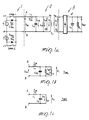
- Figure 1a illustrates the conceptual diagram of the converter according to the invention.
- said converter is studied on a basic push-pull configuration which has the least problems in driving the switches; however the converter illustrated in figure 1a is shown in a half-bridge configuration for the sake of clarity in description.
- the converter according to the invention thus essentially comprises a power supply section 1, a power transformer section 2 and a rectifier section 3, mutually cascade coupled.
- section 1 comprises a pair of constant voltage generators V which are alternately connected to the terminals A,B of section 2 by means of respective switches COMM1, COMM2, as described in detail hereinafter.
- a diode, respectively D P1 , D P2 is connected in parallel to each switch and intervenes during the opening interval of the respective switch so as to limit the voltage across the transformer, as will be described hereafter.
- Section 2 is constituted by a transformer, which in order to clarify its operation is illustrated as being constituted by an ideal transformer Ti and by dispersion and parasitary components of said transformer.
- Section 3 finally comprises a rectifier circuit 4, not shown in detail in the figure, the filtering capacitor C L and the load R L .
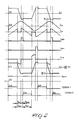
- the switches are alternately opened and closed to alternately feed a voltage V and -V to the input terminals A, B of the power transformer section 2. Both switches are also open for a set time interval.
- the conduction or closure times of said switches are chosen so that they switch at nil current, without having to introduce discrete resonance elements in order to reduce the power dissipated in the power switches, while the interval of simultaneous opening of said switches is chosen so as to make the converter self-switching and self-symmetrizing in order to solve the problems related to the possible presence of asymmetries due to the transformer, to the switches or to the secondary rectifiers.
- the wave shapes define two operating intervals: T ON , during which one of the two switches COMM1 or COMM2 is closed, and T OFF , during which both switches are open.
- T ON the equivalent circuit of figure 1b is valid, in said circuit, C eq indicating the capacitor resulting from the parallel connection of the filtering capacitor of the load, reflected on the primary winding, and the dispersion capacitor C S (such a second capacitor being however negligible with respect to the first one) and R eq indicates the resistance on the load reflected on the primary.
- Figure 1b also illustrates the magnetization inductor L p , the effect whereof being however negligible with respect to L L during the connection interval of one of the switches.
- L p has in fact a very high value with respect to L L and for the sake of simplicity it can be considered as an open circuit in parallel to the load, during the connection interval of one of the switches.
- V IN constant-value voltage
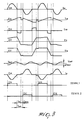
- the constant-value voltage V IN is present across the terminals A and B, enabling the current I IN to flow across L L and has a linearly rising or decreasing pattern, if there is no load (see figure 2), while, if there is a load, it has a substantially sinusoidal graph (as illustrated in figure 3).
- the interval T ON is chosen so that the current in the resonant circuit I IN is nil under load, thus closing the switch e.g. COMM1 at nil current and therefore with nil dissipated power.
- the magnetizing current I lp is fed into the diodes D P1 or D P2 connected in parallel to the switches COMM1, COMM2 (as illustrated by the currents I DPI and 1 DP2 in figure 2) when the load is zero, or into the rectifier diodes of the circuit 4 when a load is present.
- the presence of the diodes D P1 , D P2 is fundamental, as they prevent the voltage E1 and therefore E2 from continuing to rise or decrease depending on the operating state of the converter.
- T SYM is chosen so as to prevent the saturation of the transformers core due to the asymmetries caused by the construction of said transformer, by differences in the driving times of the switches, by differences in the direct voltages of the secondary rectifiers (circuit 4), by differences in the saturation voltages of the switches, and by variations in the temperature and life of the above parameters.
- T SYM is calculated by taking into account the probable extent of these asymmetries according to components data, adding a safety factor, and can typically be 20% of T AC .
- the invention fully achieves the intended aims.
- the choice of the duration of the conducting interval according to the time required by the load current to drop to zero in the resonant circuit allows to switch the power switches with nil current and therefore with nil dissipated power, consequently improving the efficiency of the converter, avoiding at the same time problems in the reliability of the resonant discrete components, in particular of the capacitor which is subject to high alternating currents.
- the push-pull operation is furthermore self-symmetrizing, eliminating the problems related to the existing asymmetries as explained above.
- the rectifier diodes furthermore have a negligible switching loss, since they are fed with a trapezoidal voltage instead of a square one (see E2), and it is not necessary to introduce additional snubber circuits as required in conventional non-resonant converters to avoid possible overload conditions.
- the circuit according to the invention furthermore has a low output impedance, in particular when the output load is low or nil, and the output signal of the converter has ripples with no high-frequency harmonic components.
- modifications and variations all of which are within the scope of the inventive concept.
- the diodes D P1 and D P2 may be intrinsic to the structure or external and faster diodes.
Landscapes
- Engineering & Computer Science (AREA)
- Power Engineering (AREA)
- Dc-Dc Converters (AREA)
Applications Claiming Priority (2)
| Application Number | Priority Date | Filing Date | Title |
|---|---|---|---|
| IT8722701A IT1225479B (it) | 1987-11-19 | 1987-11-19 | Convertitore risonante perfezionato, ad alta efficacia di conversione e bassa impedenza d'uscita |
| IT2270187 | 1987-11-19 |
Publications (2)
| Publication Number | Publication Date |
|---|---|
| EP0316892A2 true EP0316892A2 (de) | 1989-05-24 |
| EP0316892A3 EP0316892A3 (de) | 1989-12-06 |
Family
ID=11199422
Family Applications (1)
| Application Number | Title | Priority Date | Filing Date |
|---|---|---|---|
| EP88119078A Withdrawn EP0316892A3 (de) | 1987-11-19 | 1988-11-17 | Resonanzkonverter mit hohem Umwandlungswirkungsgrad und niedriger Ausgangsimpedanz |
Country Status (2)
| Country | Link |
|---|---|
| EP (1) | EP0316892A3 (de) |
| IT (1) | IT1225479B (de) |
Cited By (5)
| Publication number | Priority date | Publication date | Assignee | Title |
|---|---|---|---|---|
| EP0549920A1 (de) * | 1991-12-31 | 1993-07-07 | Alcatel Standard Electrica, S.A. | Gleichrichtersystem für aperiodisch spannungsgeschaltene Stromrichter |
| GB2457940A (en) * | 2008-02-29 | 2009-09-02 | Nujira Ltd | Filter with reduced output impedance for switched mode power supply |
| US9991805B2 (en) | 2014-02-27 | 2018-06-05 | Danmarks Tekniske Universitet | On and off controlled resonant DC-DC power converter |
| US20190068071A1 (en) * | 2017-08-31 | 2019-02-28 | Google Inc. | High-bandwith resonant power converters |
| DE102023118156A1 (de) * | 2023-07-10 | 2025-01-16 | Preh Gmbh | Vier-Quadrant-Resonanzwandler, Verfahren zu seiner Ansteuerung sowie Schaltungsanordnung für ein Kraftfahrzeug |
Family Cites Families (2)
| Publication number | Priority date | Publication date | Assignee | Title |
|---|---|---|---|---|
| US4344125A (en) * | 1981-05-14 | 1982-08-10 | Reinhard Kalfhaus | System for precise regulation of the output voltage or current of a push-pull inverter having large variations of input voltage |
| DE3142304A1 (de) * | 1981-10-24 | 1983-05-11 | AEG-Telefunken Nachrichtentechnik GmbH, 7150 Backnang | Gleichspannungswandler |
-
1987
- 1987-11-19 IT IT8722701A patent/IT1225479B/it active
-
1988
- 1988-11-17 EP EP88119078A patent/EP0316892A3/de not_active Withdrawn
Cited By (13)
| Publication number | Priority date | Publication date | Assignee | Title |
|---|---|---|---|---|
| EP0549920A1 (de) * | 1991-12-31 | 1993-07-07 | Alcatel Standard Electrica, S.A. | Gleichrichtersystem für aperiodisch spannungsgeschaltene Stromrichter |
| AU662374B2 (en) * | 1991-12-31 | 1995-08-31 | Alcatel N.V. | Rectification system for non-resonant switched converters |
| GB2457940A (en) * | 2008-02-29 | 2009-09-02 | Nujira Ltd | Filter with reduced output impedance for switched mode power supply |
| GB2457940B (en) * | 2008-02-29 | 2013-05-01 | Nujira Ltd | Improved filter for switched mode power supply |
| US8879284B2 (en) | 2008-02-29 | 2014-11-04 | Nujira Limited | Filter for switched mode power supply |
| US9608445B2 (en) | 2008-02-29 | 2017-03-28 | Snaptrack, Inc. | Filter for switched mode power supply |
| US9991805B2 (en) | 2014-02-27 | 2018-06-05 | Danmarks Tekniske Universitet | On and off controlled resonant DC-DC power converter |
| TWI689165B (zh) * | 2014-02-27 | 2020-03-21 | 丹麥商丹麥技術大學 | 開啟及關閉控制的共振直流對直流電源轉換器及操作方法 |
| US20190068071A1 (en) * | 2017-08-31 | 2019-02-28 | Google Inc. | High-bandwith resonant power converters |
| WO2019045789A1 (en) * | 2017-08-31 | 2019-03-07 | Google Llc | RESONANT POWER CONVERTERS WITH HIGH BANDWIDTH |
| US10277140B2 (en) | 2017-08-31 | 2019-04-30 | Google Llc | High-bandwith resonant power converters |
| TWI700879B (zh) * | 2017-08-31 | 2020-08-01 | 美商谷歌有限責任公司 | 高頻寬共振功率轉換器及用於功率轉換之方法 |
| DE102023118156A1 (de) * | 2023-07-10 | 2025-01-16 | Preh Gmbh | Vier-Quadrant-Resonanzwandler, Verfahren zu seiner Ansteuerung sowie Schaltungsanordnung für ein Kraftfahrzeug |
Also Published As
| Publication number | Publication date |
|---|---|
| IT8722701A0 (it) | 1987-11-19 |
| IT1225479B (it) | 1990-11-14 |
| EP0316892A3 (de) | 1989-12-06 |
Similar Documents
| Publication | Publication Date | Title |
|---|---|---|
| CN100466446C (zh) | 直流电压转换成交流电压的方法、电路布置结构和逆变器 | |
| US5761055A (en) | Driving pulse output limiting circuit | |
| CA1151728A (en) | Semiconductor switching circuit with clamping and energy recovery features | |
| US6611444B2 (en) | Zero voltage switching DC-DC converter | |
| US5694307A (en) | Integrated AC/DC and DC/DC converter | |
| US11070135B2 (en) | Converter with soft-start period of output voltage | |
| US5166869A (en) | Complementary electronic power converter | |
| KR20110110805A (ko) | Dc/dc-변환기 및 ac/dc-변환기 | |
| US7609532B1 (en) | Phase-shifted PWM bridge with switchable inductors to maintain zero-voltage switching at light load | |
| JPH04156274A (ja) | 電力変換装置 | |
| US5640318A (en) | Forward converter for off-line applications | |
| CN112640280B (zh) | 具有控制装置和无源频率滤波器的多相多级变流器以及用于控制多相多级装置变流器的方法 | |
| EP0316892A2 (de) | Resonanzkonverter mit hohem Umwandlungswirkungsgrad und niedriger Ausgangsimpedanz | |
| US20220224224A1 (en) | Multiphase interleaved forward power converters including clamping circuits | |
| US6600667B2 (en) | Electronic transformer | |
| CA1266505A (en) | D.c. to d.c. converter | |
| US4980813A (en) | Current fed push pull power converter | |
| US11527963B2 (en) | Control unit for improving conversion efficiency | |
| JP2020174465A (ja) | 三相交流用の絶縁型力率改善装置 | |
| US6008997A (en) | Series resonant converter with inherent short circuit protection | |
| JP3327754B2 (ja) | 半導体スイッチング素子のゲート駆動装置 | |
| KR20110002223A (ko) | 직렬공진형 컨버터 | |
| RU2043695C1 (ru) | Импульсный источник вторичного электропитания | |
| US20060164869A1 (en) | Inverter | |
| JP3259337B2 (ja) | 電力変換装置 |
Legal Events
| Date | Code | Title | Description |
|---|---|---|---|
| PUAI | Public reference made under article 153(3) epc to a published international application that has entered the european phase |
Free format text: ORIGINAL CODE: 0009012 |
|
| AK | Designated contracting states |
Kind code of ref document: A2 Designated state(s): DE FR |
|
| PUAL | Search report despatched |
Free format text: ORIGINAL CODE: 0009013 |
|
| AK | Designated contracting states |
Kind code of ref document: A3 Designated state(s): DE FR |
|
| STAA | Information on the status of an ep patent application or granted ep patent |
Free format text: STATUS: THE APPLICATION IS DEEMED TO BE WITHDRAWN |
|
| 18D | Application deemed to be withdrawn |
Effective date: 19900607 |