EP0316624A2 - Abbildungs- und Inspektionapparat und Verfahren - Google Patents
Abbildungs- und Inspektionapparat und Verfahren Download PDFInfo
- Publication number
- EP0316624A2 EP0316624A2 EP88117760A EP88117760A EP0316624A2 EP 0316624 A2 EP0316624 A2 EP 0316624A2 EP 88117760 A EP88117760 A EP 88117760A EP 88117760 A EP88117760 A EP 88117760A EP 0316624 A2 EP0316624 A2 EP 0316624A2
- Authority
- EP
- European Patent Office
- Prior art keywords
- edge
- peripheral
- outputs
- output
- central
- Prior art date
- Legal status (The legal status is an assumption and is not a legal conclusion. Google has not performed a legal analysis and makes no representation as to the accuracy of the status listed.)
- Withdrawn
Links
Images


Classifications
-
- G—PHYSICS
- G01—MEASURING; TESTING
- G01B—MEASURING LENGTH, THICKNESS OR SIMILAR LINEAR DIMENSIONS; MEASURING ANGLES; MEASURING AREAS; MEASURING IRREGULARITIES OF SURFACES OR CONTOURS
- G01B11/00—Measuring arrangements characterised by the use of optical techniques
- G01B11/02—Measuring arrangements characterised by the use of optical techniques for measuring length, width or thickness
- G01B11/028—Measuring arrangements characterised by the use of optical techniques for measuring length, width or thickness by measuring lateral position of a boundary of the object
Definitions
- This invention relates to object inspection techniques, and more particularly to optical apparatus and method for detecting edges of parts or objects with high precision and repeatability.
- One basis for measuring the dimensions of a part or object is finding suitable edges or surfaces accurately and repeatably. Many parts are contact-sensitive or moving too fast in automated handling for contact methods. For low-cost manual operations, this is usually accomplished with a microscope having calibrated cross-hairs in the eyepiece. The operator judges the location of the edges of the part and then aligns the cross-hairs with such edges in order to read the dimension. This labor-intensive process is subjective and susceptible to operator fatigue and variances.
- CMMs Coordinate Measuring Machines
- AOI Automated Optical Inspection
- AOI is a desirable "in-process" method of inspection in automated manufacturing that can remove the subjectivity of set-up and inspections during fabrication while allowing corrections of measurement parameters to be made immediately, resulting in more precise parts at higher yields in less time.
- AOI is an optical, non-contact technique, it removes many of the speed and part accessibility limits usually encountered in conventional measuring techniques and provides precision and accuracy previously unattainable, for example, with contact inspection techniques.
- Various optical, non-contacting measuring and inspection schemes are described in the literature (see, for example, U.S. patents 4,422,763; 4,384,195; 4,583,854; 3,879,131; 4,201,476; 3,856,412; 4,272,190; 4,597,668; 4,624,563; and 4,427,296).
- Optical measurement techniques are ideally suited for high-speed precision fabrication of metal parts, electronic assemblies, semiconductor components, and for numerous other manufacturing tasks such as alignment, inspection, tracking, and the like, within diverse segments of commerce.
- measurement microscopes as described in the literature, are commonly used in the inspection or alignment of small and delicate parts. They are often equipped with "encoders" which precisely display the position of a part with respect to the cross-hairs seen through the eyepiece.
- a camera port is typically used to mount a video camera which aids the operator in the inspection process. Because these camera ports are well-standardized, any instrument with such a feature can support a variety of accessories, including an edge-finding accessory of the type later described herein.
- an improved edge-detecting method and apparatus includes a laser for producing a specially-formatted beam, a microscope-type optical system, and a segmented detector for locating the edges of parts or objects with high precision and repeatability and without the interpolative error between data bits commonly associated with digital systems.
- the laser provides a very high concentration of light in a well-controlled zone for high inspection sensitivity. This zone is a constant percentage of the field of view, regardless of the power of the objective lens in the optical system. That is, the spot size of the beam in the field of view is not dependent upon objective magnification. This zone also provides a "smoothing" effect over rough edges when viewed at high magnification.
- the accuracy and resolution increases as the power of the objective increases and the area of the laser beam at the sample decreases.
- the laser beam exhibits peak power or intensity at its center which is utilized to provide maximum signal change as an edge under inspection crosses the center of the beam. Its single wavelength allows viewing of the part or object under ambient light which will not affect the precision of the edge detector.
- the detector according to the present invention includes a pattern of active elements which provide electrical signals that represent the portion of the beam reflected back through the optical system from the sample part.
- the pattern of active elements makes maximum use of the laser beam intensity profile for enhanced sensitivity to movement of reflective edges. Since the present invention spatially integrates the beam power over the dimensions of the beam, the the effects of rough edges and surfaces tend to be averaged or smoothed out.
- Analog electronics decode the detector signals into virtual digital "on//off" output when either a vertical or horizontal edge condition is detected that matches established signal limits.
- the detector and electronics can sense edges along X and Y axes independently and simultaneously.
- the analog circuitry is not computationally limited and permits edge detection in less than 1 microsecond for measurements "on-the-fly” at rates of movement of the sample parts of more than 1 meter/second.
- the method and apparatus of the present invention tolerates changes in distance from the objective lens to the sample part, but there are trade-offs between edge-finding resolution and depth-of-focus that depend upon the magnifying power of the objective lens.
- An "autofocus" system may be provided to maintain optimal working distance and to provide proximity measurement capability as well. As the contrast ratio between reflections received from sample starts and the background beyond the edge diminishes below limits, an indicator of insufficient contrasts is provided to advise the operator that measurement under these conditions may have poor measurement accuracy.
- the geometry of the edge features are a large fraction of the radius of the laser beam.
- the operator is alerted that, for this type of edge, the magnifying power of the objective lens should be reduced in order to capture more of the edge within the beam zone (with slightly lower edge-finding resolution and repeatability).
- the spot size of the beam may be changed by conventional "zoom"-type optics.
- the beam location is fixed and the sample part is moved around under the measurement lens of the optical system.
- the edge positions thus accurately determined yield the distance or measurement between edges as a function of the translations of the supporting stage, and encoders coupled to the supporting stage provide the indication of the dimensions of a sample part between detected edges.
- Sample parts being sensed in sequence should, of course, be separated by at least one spot-size diameter for unambiguous detection.
- the present invention can thus form an integral part of an inspection system or process-control scheme in which the precise detection of an edge is essential.
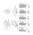
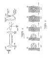
- FIG. 1 there is shown a simplified pictorial diagram of an optical system according to one embodiment of the present invention in which the portion of a laser beam reflected from a sample part or object 9 is received by an optical sensor or detector 41.
- a continuous-wave He Ne gas laser 13 is disposed to supply a laser beam 15 through a beam-formatting lens 16 to an optical beam splitter 17 (e.g., half-mirrored surface) for deflection through relay more lens 12 and objective lens 14 toward the sample 9 which is oriented to move on a supporting stage 19 for movement along orthogonally-oriented X and Y axes.
- an optical beam splitter 17 e.g., half-mirrored surface
- Suitable encoders of conventional design may be linked to the stage to indicate (electrically or mechanically) the movement of the stage 19 along respective axes in traversing the distances between sets of edges of the sample part 9.
- the reflected beam from sample part 9 passes through the beam splitter 17 and imaging lens 18 and transmission filter 20 to the detector 41.
- the transmission filter 20 may be interposed to limit the transmission of light to only the wavelength of laser 13.
- the combination of the relay lens 12 and the formatting lens 16 provide constant spot size as a percentage of field given regardless of objective lens 14 magnification.
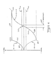
- the beam 15 from laser 13 has a substantially Gaussian power density or intensity distribution with distance across the dimension thereof, as illustrated by the curve 21 of Figure 2. It should be noted that this power density distribution is substantially symmetrical with a peak of intensity near the center of the curve. Also, it should be noted that the integral with distance of the power density distribution across the laser beam (illustrated by curve 23 on a different vertical scale in Figure 2) has a maximum rate of change, or slope, at the center peak.
- This maximum rate of change of the integrated power density across the laser beam is utilized in the present invention to provide precision edge detection of a sample part within narrow limits 25 of electrical noise, switching delays, and the like, and with highest sensitivity to positional change across the center of the beam, and this translates to narrow limits of position error 24 within the central area of the laser beam 15. If such laser beam 15 is supplied to a sample part at an edge thereof, then the power density distribution across the beam (reflected or transmitted) on opposite sides of an edge of the part centered in the beam would appear as illustrated in Figure 3.
- the curve 29 of Figure 3 illustrates the reflected or transmitted power density distribution across an edge (which is at least longer than the diameter of the beam), and illustrates the maximum differential intensity across the edge of the sample as an indication of the contrast ratios present across an edge.
- the graph of contrast ratio across the edge will not appear as a disfunctional curve 29 but rather will appear as a continuous curve with distinct upper and lower inflection points in a wider region of transition over X distance 33 from the peak intensity 35 to the reference level 37 of no reflection or no transmission.
- the differences between the power densities in a laser beam on opposite sides of an edge as the edge of the sample part moves through the beam establish high contrast ratios across the edge.
- the slope or rate of change of differences of power densities on opposite sides of an edge diminishes with diminished contrast ratio.
- a wide range of contrast ratios i.e., wide range of edge conditions
- the center of the beam is used to find the edge of the sample since most of the center region of the beam is in the region of highest slope of the integrated power density (curve 23 of Figure 2), and the differences of power densities across the edge have the greatest slopes or rates of change where high contrast ratios are present across the edge.
- the detector differential signal is compared with a reference signal.
- This reference can be “captured” in a variety of conventional analog, digital or hybrid “sample and hold” circuits.
- An acceptance “window” can be devised as a percentage of the reference level such that if the signal received from the sample part falls between the window limits, the edge condition is assumed to have been met.
- Variances in absolute laser beam power, sample surface reflectance, and electrical noise, as well as depth of focus sensitivity make a fixed reference subject to failure in finding edges because of small variances in a less-than-average sample edge for use as a 'reference' edge.
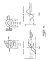
- the laser beam is configured to exhibit substantially Gaussian power density or intensity distribution across its width, and this characteristic is used to advantage according to the present invention by employing a beam detector, as illustrated in Figure 4(a), which includes several active segments that are patterned and dimensioned relative to the dimensions of the laser beam.
- the detector 41 includes a central active segment E43 which has a diameter that is substantially equal to that diameter 51 of the laser beam at which the condition of substantially one-half the spatially-integrated power is satisfied.
- This one-half-power dimension on the power-density distribution profile 21 of a laser beam is illustrated in Fig. 5(a).
- the remaining active segments A44, B45, C47, and D49 are arranged concentrically about the center segment E43 and within the outer diameter 53 of the laser beam.
- Opposite pairs of peripheral segments are oriented in alignment with the X and Y axes of movement of the sample part 9.
- these dimensions may be directly correlated or may be scaled up or down by suitable optical magnification.
- the power density distribution across the reflected beam may appear as illustrated in Figure 4(b) where the diameter of the center segment E43 is less than the diameter of the laser beam at the half-power diameter thereof, as previously explained, and such condition will diminish edge sensitivity for reasons as later described herein.
- the resulting signal level becomes a valid reference level.
- This will have an "in range to edge” level that is dependent upon the angle which the edge makes to the X or Y axis.
- the difference between diametrically-opposed outer segment is used to lower or bias the signal from the central segment. This permits use of many well-known "zero crossing" techniques to determine when the edge condition is within given limits. For edges close to 45° from X or Y axes, 8 segments, around the perimeter rather than 4 can be used, and the largest differential between diametric opposite segments can be used as the reference in that case.
- the outer active segments A44, B45, C47, and D49 are oriented in quadrants around the center segment E43, and are angularly positioned so that opposite pairs of areas are substantially aligned with the orthogonal X and Y axes of relative movement of sample part and beam.
- Multi-segment detectors similar to detector 41 are described in the literature (see, for example, U.S. patent 3,435,232).
- a reflective sample part 9 supported on stage 19 to move along the X axis from left to right relative to the detector 41 causes left segment D49 to be illuminated initially as the right edge 55 of the sample part to be detected enters the field of view of the detector for reflections from the part 9.
- the edge 55 to be detected may be considered to be the left edge of a part that is moving from left to right to expose the left segment D49 first.
- the illuminated area of active segment D (of conventional photo-responsive design) produces a signal that increases with distance traversed as more area of the active segment receives the reflected laser beam.
- the opposite-pair segment B aligned with segment D along the X axis will similarly produce increased output signal as its active area later receives the reflected laser beam.
- the signal gain, or weighting factor, for signal from segment E may be set at twice the gain for signals from segment A or B or C or D in order to establish the signal from exactly one-half of segment E under full illumination to be substantially equal to the signal from area D (or B) under full illumination.
- the dimensions of the active segments may be selected such that the output of Central Segment E is 1/3 of the total beam power, or 1/2 of the combined output of A + B + C + D fully illuminated. Therefore, the combined signal of E - (B + D) illustrated by the curve 59 of Figure 6 represents the integral (from level 61) of the reflected detected laser beam power with distance of the edge 55 moving across the area of segment E.
- the signal from segment E equals the inverse signal from segment D to provide a zero-level crossing at maximum rate of change (or slope) of signal with distance moved by the edge 55.
- Segment B may be sending background illumination which can reduce detectable contrast, so the contained signals from segments B + D is used as the reference condition along the X-axis direction.
- Suitable zero-crossing detection circuits of conventional design may be used to produce an output upon zero-crossing of the signal E - (B + D), within the narrow limits 63 of noise signals or selected limit signals about zero level, as an indication of the precise alignment of the edge 55 at the position of exact center of segment E, as shown in Figure 5(d).
- edge-detection sensitivity of about 1 micron of movement.
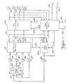
- Amplifiers 81 - 89 are connected to receive the signals from the segments A - E, respectively, of the detector 41 and are set with equal gains amplifiers 81-87 and with twice such gain in amplifier 89 for reasons as previously discussed with reference to Figures 5 and 6.
- equal gains may be applied to signals derived from segments that are sized to integrate, in the central segment, twice the beam power of an outer segment when fully illuminated.
- the amplified signals are supplied to the inputs of the sum-and-difference amplifier 91 to yield the selected outputs (A + C) 93, (A - C) 95, (B + D) 97, (B - D) 99, and (A + B + C + D) 101.
- the outputs 95 and 99 are applied to the edge orientation logic circuit 103, and the outputs 93 and 97 are applied to the edge condition logic circuit 105.
- the edge orientation logic circuit receives X reference and Y reference signals 104, 106 and may include conventional analog logic circuitry for producing outputs 107, 109, 111, and 113 indicative of upper, lower, left, and right edges, respectively, according to the following logic conditions.
- the edge-detection system of the embodiment of the present invention relies upon the Gaussian distribution of light intensity or power density across a laser beam to provide accurate processing of analog signals indicative of the position of an edge of a sample part within the laser beam.
- Simple analog processing and logical analysis of signals from a multi-segment detector provide unambiguous indication of left or right, upper or lower edges of the sample part, with high positional accuracy as the start is moved through the laser beam aligned (either in reflective or transmissive mode) with the detector.
- High contrast ratios across the edge of the sample part provide greatest sensitivities to positional change across the laser beam to establish highly repeatable and highly accurate edge positional indications.
- a white-light source 140 may be used to project an image of the object onto a sheet 142 of photo-reflective material (such as photoconductor-coated lithium niobate) so that the image of an edge is converted to a real reflecting edge 144 on the photo-reflective crystal 142.
- photo-reflective material such as photoconductor-coated lithium niobate
- the detector configuration of the present invention can also be used to determine how close the edge of the object is to the focal point of the objective lens.
- the beam power at the focal point is dominantly concentrated at the center of the beam, and this permits auto-focusing (Z focus ) of the optical system with respect to such Z focus reference condition to assure edge detection within the range of accuracy.
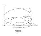
- This condition occurs, as illustrated in Figure 8, when: [(A + B + C + D)/2] - E ⁇ Z focus (Eq. 10)
- the orientation of a reflective edge at 45° with respect to the X and Y orthogonal axes yields an indeterminate condition of the power in the outer detectors equalling the power in the center detector.
- This uncertainty can be resolved in one embodiment of the present invention by forming orthogonally-oriented gaps 146 between outer segments of the detector, as illustrated in Figure 10(a), or by forming a concentric, "bull's-eye" pattern of detector segments, as illustrated in the embodiment of Figure 10(b).
- the detector of Figure 10(a) collects less of the total power in the laser beam and thus is more susceptible to noise for example, attributable to scattering from surface roughness.
- the "bull's-eye" pattern of Figure 10(b) substantially all of the laser-beam power is detected, but the response of the outer ring 148 does not completely plateau (154 in Figure 10(c)) when the edge condition is met.
- W is the diameter of the laser beam out to the dimension of the beam at which the intensity level equals (Eq. 11) where I0 is the maximum beam intensity at approximately the center, and the outer diameter d of the detector is approximately three times the beam width W.
- the diameter of the center segment 150 is set at approximately .90 times W, and the beam power detected by center segment 150 is equal to 2 times the sum of the beam power detected by segments A, B, C or D.
- the diameter of the inner segment 152 is 1.18 times W such that the beam power detected by the inner segment 152 equals the beam power detected by the outer segment 148.
- the relative intensities of beam detected by the detector illustrated in Figure 10(b) is illustrated in the graph of Figure 10(c), and the differential intensities of beam detected by such detector is illustrated in the graph of Figure 10(d).
- the detector embodiments described above also work adequately well on beams of light with non-uniform intensity distribution over the beam width (for example, 'top-hat'-shaped distribution) with well-defined peripheral boundaries.
- a source of a beam having non-Gaussian or incoherent power distribution such as from a laser diode or light-emitting diode or even a white-light source
- good zero-crossing, edge-detection response is still achieved according to the present invention.
- the additional requirement is established that the detected light levels at either side of the edge have minimum differential. Otherwise, there would need to be an absolute zero-crossing range for each sample of reflectivity.
- FIG 11 there is shown an embodiment of a detector according to the present invention in which the outer ring of the "bull's-eye" pattern is again segmented in quadrants A, B, C and D, with gaps therebetween oriented along the X and Y orthogonal axes.
- progression of an edge across the detector with a non-orthogonal orientation yields a partial leveling 154 of the sum of the outer segments, as illustrated in the graph of Figure 10(c)
- progression of an edge across the detector with an orthogonal orientation yields a complete leveling 156 of the sum of the outer segments near edge crossing of the X or Y axis, as illustrated in the graph of Figure 14.
- This embodiment of the present invention provides the advantages of generating information about angular orientation of the edge as well as using the entire beam power in the zero-crossing signals for less sensitivity to noise (for example, from surface-roughness scattering).
- the gaps between outer segments need only be about .005" for precision operation as described, as well as for ease of manufacture.
- the detector may be found on multiple levels with active Segments A and C fabricated on a plateau or mesa, say, above Segment E, and with Segments B and D fabricated on a planes (or planes) below Segment E to enable the edges of those active segments to be substantially vertically aligned and still be insulated from the adjacent segments.
- Similar considerations apply for sensing angular edge orientation within each of the four quadrants. For this angular information, the beam is considered rotationally symmetrical, and the first outer segment in a quadrant, as illustrated in Figure 12, in which the edge appears is identified.
- the percentage of one-half the response of central segment E by which such outer segment is illuminated at the edge condition provides the requisite information about angular orientation of the edge, as follows: Then, it can be shown that the angle through A is where r is the radius from inner to outer edge of the Segments A, B, C and D, and I0 is the maximum beam intensity and W is the beam width as previously described.
- the illumination level in the next quadrant oriented counterclockwise from the certain quadrant is minimal because it is not aligned with the edge.
- the angle of orientation of an edge with respect to the other quadrants can also be similarly determined.
Landscapes
- Physics & Mathematics (AREA)
- General Physics & Mathematics (AREA)
- Length Measuring Devices By Optical Means (AREA)
- Investigating Materials By The Use Of Optical Means Adapted For Particular Applications (AREA)
Applications Claiming Priority (4)
| Application Number | Priority Date | Filing Date | Title |
|---|---|---|---|
| US07/120,130 US4856902A (en) | 1987-11-13 | 1987-11-13 | Imaging and inspection apparatus and method |
| US120130 | 1987-11-13 | ||
| US179641 | 1988-04-08 | ||
| US07/179,641 US4906097A (en) | 1987-11-13 | 1988-04-08 | Imaging and inspection apparatus and method |
Publications (2)
| Publication Number | Publication Date |
|---|---|
| EP0316624A2 true EP0316624A2 (de) | 1989-05-24 |
| EP0316624A3 EP0316624A3 (de) | 1990-12-27 |
Family
ID=26818081
Family Applications (1)
| Application Number | Title | Priority Date | Filing Date |
|---|---|---|---|
| EP19880117760 Withdrawn EP0316624A3 (de) | 1987-11-13 | 1988-10-25 | Abbildungs- und Inspektionapparat und Verfahren |
Country Status (3)
| Country | Link |
|---|---|
| US (1) | US4906097A (de) |
| EP (1) | EP0316624A3 (de) |
| JP (1) | JPH01239404A (de) |
Cited By (5)
| Publication number | Priority date | Publication date | Assignee | Title |
|---|---|---|---|---|
| EP0484665A3 (en) * | 1990-10-31 | 1993-07-07 | Shin-Etsu Handotai Company, Limited | Pattern shift measuring method |
| DE19713336C1 (de) * | 1997-03-29 | 1998-07-02 | Zeiss Carl Jena Gmbh | Ortsempfindlicher fotoelektrischer Sensor |
| EP0903560A3 (de) * | 1997-09-23 | 2000-11-15 | Kai Stapelfeldt | Optoelektronische Sensoreinrichtung |
| US6665064B2 (en) | 2000-11-30 | 2003-12-16 | Prüftechnik Dieter Busch AG | Electrooptical measurement device for ascertaining the relative position of bodies or of surface areas of these bodies |
| WO2004063663A3 (en) * | 2003-01-08 | 2004-11-04 | Honeywell Int Inc | Opto-electronic transmissive edge location sensor |
Families Citing this family (8)
| Publication number | Priority date | Publication date | Assignee | Title |
|---|---|---|---|---|
| US5440338A (en) * | 1993-05-11 | 1995-08-08 | Spiricon, Inc. | Method and apparatus for improving dimensional measurements made with video cameras |
| US5418562A (en) * | 1993-05-11 | 1995-05-23 | Spiricon, Inc. | Method and apparatus for increasing the accuracy of dimensional measurements made with video cameras |
| US6388809B1 (en) * | 1997-10-29 | 2002-05-14 | Digital Optical Imaging Corporation | Methods and apparatus for improved depth resolution use of out-of-focus information in microscopy |
| US6987893B2 (en) * | 2001-01-05 | 2006-01-17 | Lg Electronics Inc. | Image interpolation method and apparatus thereof |
| US6809823B2 (en) * | 2001-09-28 | 2004-10-26 | Agilent Technologies, Inc. | Method for the calibration and alignment of multiple multi-axis motion stages for optical alignment to a planar waveguide device and system |
| WO2013150585A1 (ja) * | 2012-04-02 | 2013-10-10 | 三菱電機株式会社 | エッジ検出装置 |
| US8755114B1 (en) | 2013-06-14 | 2014-06-17 | Computer Power Supply, Inc. | Apparatus for aiding manual, mechanical alignment of optical equipment |
| CN114061460B (zh) * | 2021-11-18 | 2023-06-09 | 内蒙古工业大学 | 一种主轴内置型风力发电机组齿轮箱轴向位移监测装置 |
Family Cites Families (17)
| Publication number | Priority date | Publication date | Assignee | Title |
|---|---|---|---|---|
| US3435232A (en) * | 1966-03-03 | 1969-03-25 | Hewlett Packard Co | Beam position detector |
| US3856412A (en) * | 1973-06-08 | 1974-12-24 | Zygo Corp | Optical noncontacting gauge |
| US3879131A (en) * | 1974-02-06 | 1975-04-22 | Bell Telephone Labor Inc | Photomask inspection by real time diffraction pattern analysis |
| US4201476A (en) * | 1978-01-05 | 1980-05-06 | The Austin Company | Laser dimension gauge |
| US4272190A (en) * | 1978-08-14 | 1981-06-09 | Typalogics | Optical measuring system |
| US4547895A (en) * | 1978-10-30 | 1985-10-15 | Fujitsu Limited | Pattern inspection system |
| US4422763A (en) * | 1978-12-08 | 1983-12-27 | Rca Corporation | Automatic photomask alignment system for projection printing |
| US4384195A (en) * | 1980-06-09 | 1983-05-17 | The Coe Manufacturing Company | Edge-responsive apparatus for counting conveyor-transported articles |
| US4427296A (en) * | 1981-09-03 | 1984-01-24 | Zygo Corporation | Electro-optical measuring system |
| US4433912A (en) * | 1982-01-21 | 1984-02-28 | Dr. Ing. Rudolf Hell Gmbh | Method and a circuit for determining a contour in an image |
| JPS58173408A (ja) * | 1982-04-05 | 1983-10-12 | Mitsutoyo Mfg Co Ltd | 光学式測定機器におけるエツジ検出装置 |
| US4583854A (en) * | 1982-07-15 | 1986-04-22 | General Electric Company | High resolution electronic automatic imaging and inspecting system |
| US4597668A (en) * | 1983-04-26 | 1986-07-01 | Tokyo Shibaura Denki Kabushiki Kaisha | Device for checking positional accuracy |
| US4624563A (en) * | 1983-12-05 | 1986-11-25 | The United States Of America As Represented By The Secretary Of The Army | Wide field of view remote laser position sensor |
| US4744663A (en) * | 1984-12-14 | 1988-05-17 | Nippon Kogaku K.K. | Pattern position detection apparatus using laser beam |
| JPH0814484B2 (ja) * | 1985-04-09 | 1996-02-14 | 株式会社ニコン | パタ−ン位置測定装置 |
| US4713533A (en) * | 1986-01-03 | 1987-12-15 | Westinghouse Electric Corp. | Concentric detector array and associated hybrid signal processing for coarse and fine electro-optical tracking |
-
1988
- 1988-04-08 US US07/179,641 patent/US4906097A/en not_active Expired - Fee Related
- 1988-10-25 EP EP19880117760 patent/EP0316624A3/de not_active Withdrawn
- 1988-11-14 JP JP63287497A patent/JPH01239404A/ja active Pending
Cited By (6)
| Publication number | Priority date | Publication date | Assignee | Title |
|---|---|---|---|---|
| EP0484665A3 (en) * | 1990-10-31 | 1993-07-07 | Shin-Etsu Handotai Company, Limited | Pattern shift measuring method |
| DE19713336C1 (de) * | 1997-03-29 | 1998-07-02 | Zeiss Carl Jena Gmbh | Ortsempfindlicher fotoelektrischer Sensor |
| EP0903560A3 (de) * | 1997-09-23 | 2000-11-15 | Kai Stapelfeldt | Optoelektronische Sensoreinrichtung |
| US6665064B2 (en) | 2000-11-30 | 2003-12-16 | Prüftechnik Dieter Busch AG | Electrooptical measurement device for ascertaining the relative position of bodies or of surface areas of these bodies |
| WO2004063663A3 (en) * | 2003-01-08 | 2004-11-04 | Honeywell Int Inc | Opto-electronic transmissive edge location sensor |
| US6891181B2 (en) | 2003-01-08 | 2005-05-10 | Honeywell International Inc. | Opto-electronic transmissive edge location sensor |
Also Published As
| Publication number | Publication date |
|---|---|
| JPH01239404A (ja) | 1989-09-25 |
| EP0316624A3 (de) | 1990-12-27 |
| US4906097A (en) | 1990-03-06 |
Similar Documents
| Publication | Publication Date | Title |
|---|---|---|
| US5129010A (en) | System for measuring shapes and dimensions of gaps and flushnesses on three dimensional surfaces of objects | |
| EP1828713B1 (de) | Dünnschicht-dickenmessungsverfahren und -vorrichtung | |
| US5410410A (en) | Non-contact type measuring device for measuring three-dimensional shape using optical probe | |
| CA1059752A (en) | Gauging surfaces by remotely tracking multiple images | |
| EP0279347B1 (de) | Optische Achsenverschiebungsfühler | |
| US4498776A (en) | Electro-optical method and apparatus for measuring the fit of adjacent surfaces | |
| US4906097A (en) | Imaging and inspection apparatus and method | |
| US5208451A (en) | Method and apparatus for automated focusing of an interferometric optical system | |
| EP0627610B1 (de) | Kontaktloser zweistufiger Detektionspositionierungsapparat | |
| CN118914228A (zh) | 一种具有二维角度测量调整的大量程调焦系统 | |
| US5459576A (en) | Differential phase contrast inspection system | |
| US4856902A (en) | Imaging and inspection apparatus and method | |
| US5298976A (en) | Method and apparatus for measuring surface distances from a reference plane | |
| JP3180091B2 (ja) | レーザーオートフォーカスによる非接触寸法測定方法 | |
| JPH0123041B2 (de) | ||
| JP3112219B2 (ja) | 移動検出方法及び検出器 | |
| JPH07332954A (ja) | 変位傾斜測定方法および装置 | |
| Mashimo et al. | Development of optical noncontact sensor for measurement of three-dimensional profiles using depolarized components of scattered light | |
| Hanke | Applying optical measurement techniques | |
| JPH05231848A (ja) | 光学式変位センサ | |
| JP2591143B2 (ja) | 三次元形状測定装置 | |
| Ahlers | Electro-Optical Sensors In Industrial Applications | |
| JP3068695B2 (ja) | ダハ面測定装置 | |
| JP2866566B2 (ja) | 三次元形状入力装置 | |
| JPS5826325Y2 (ja) | 位置検出装置 |
Legal Events
| Date | Code | Title | Description |
|---|---|---|---|
| PUAI | Public reference made under article 153(3) epc to a published international application that has entered the european phase |
Free format text: ORIGINAL CODE: 0009012 |
|
| AK | Designated contracting states |
Kind code of ref document: A2 Designated state(s): AT CH DE FR GB LI |
|
| RAP1 | Party data changed (applicant data changed or rights of an application transferred) |
Owner name: METRONICS, INC. |
|
| PUAL | Search report despatched |
Free format text: ORIGINAL CODE: 0009013 |
|
| AK | Designated contracting states |
Kind code of ref document: A3 Designated state(s): AT CH DE FR GB LI |
|
| RHK1 | Main classification (correction) |
Ipc: G01B 11/00 |
|
| STAA | Information on the status of an ep patent application or granted ep patent |
Free format text: STATUS: THE APPLICATION IS DEEMED TO BE WITHDRAWN |
|
| 18D | Application deemed to be withdrawn |
Effective date: 19910628 |