EP0315435A2 - Bildwandlerröhre zur Aufnahme von mit hoher Geschwindigkeit ablaufenden Vorgängen - Google Patents
Bildwandlerröhre zur Aufnahme von mit hoher Geschwindigkeit ablaufenden Vorgängen Download PDFInfo
- Publication number
- EP0315435A2 EP0315435A2 EP88310317A EP88310317A EP0315435A2 EP 0315435 A2 EP0315435 A2 EP 0315435A2 EP 88310317 A EP88310317 A EP 88310317A EP 88310317 A EP88310317 A EP 88310317A EP 0315435 A2 EP0315435 A2 EP 0315435A2
- Authority
- EP
- European Patent Office
- Prior art keywords
- photocathode
- grid
- electrode
- electrodes
- grid electrode
- Prior art date
- Legal status (The legal status is an assumption and is not a legal conclusion. Google has not performed a legal analysis and makes no representation as to the accuracy of the status listed.)
- Granted
Links
Images

Classifications
-
- H—ELECTRICITY
- H01—ELECTRIC ELEMENTS
- H01J—ELECTRIC DISCHARGE TUBES OR DISCHARGE LAMPS
- H01J31/00—Cathode ray tubes; Electron beam tubes
- H01J31/08—Cathode ray tubes; Electron beam tubes having a screen on or from which an image or pattern is formed, picked up, converted, or stored
- H01J31/50—Image-conversion or image-amplification tubes, i.e. having optical, X-ray, or analogous input, and optical output
- H01J31/501—Image-conversion or image-amplification tubes, i.e. having optical, X-ray, or analogous input, and optical output with an electrostatic electron optic system
- H01J31/502—Image-conversion or image-amplification tubes, i.e. having optical, X-ray, or analogous input, and optical output with an electrostatic electron optic system with means to interrupt the beam, e.g. shutter for high speed photography
Definitions
- This invention relates to electron optical image tubes of the type known as streaking or framing image tubes, and more particularly to the gating of such image tubes.
- a streaking or framing image tube normally includes an electrode assembly for forming a focussed image on the screen of the tube, the electrode assembly normally includes one or more focus electrodes which by application of the appropriate potential(s), shapes the electric field between photocathode and anode in such a way so as to produce a correctly focussed image.
- the invention is particularly although not exclusively intended for streaking or framing image tubes in which the image on the screen is inverted relative to the optical image applied to the photocathode.
- GB-A-1 458 399 describes a streaking or framing image tube in which two mesh electrodes are interposed between the photocathode and the focussing electrode.
- GB-A-2 171 553 a method of gating such a two mesh streaking or framing image tubes is described.
- the method comprises raising and lowering the potential of the first grid, which is closest to the photocathode, over a short interval of time, to gate the electron beam on and off over the said interval, the second grid being held at a constant potential chosen so that the focussing conditions for the image tube are satisfied.
- the streaking or framing image tube is constructed so that it has three "grid" electrodes disposed between the photocathode and the focus electrode assembly as shown in Fig 1.
- the tube is regarded as operated in the "normal gated off” or “standby” mode when the potentials are as indicated in Fig 2. In this situation electrons which are emitted from the photocathode 4 and pass through "grid” electrode 1 are returned to "grid” electrode 1 by the influence of the electric field between "grid” electrodes 1 and 2.
- the image tube is "gated on” by the application of a voltage pulse to "grid" electrode 2 such that during the duration of the pulse the potential of "grid” electrode 2 is sufficiently greater than that of photocathode 4 such that electrons emitted from photocathode 4 which pass through “grid” electrode 1 can now pass through “grid” electrodes 2 and 3 to reach the screen 12.
- the image tube is "gated off” by applying to the photocathode 4 an identical or at least very similar voltage pulse to that used to "gate” on the tube so that during the duration of the pulse the potential of the photocathode 4 is held at a value about that of "grid” electrode 1 such that electrons emitted from the photocathode 4 are returned to photocathode 4 by the action of the retarding field between photocathode 4 and "grid" electrode 1.
- the "grid” electrode 1 is held at a constant potential during all the modes of tube operation.
- “grid” electrode 3 is held at a constant potential during all the modes of tube operation, the potential being that required for optimum focus of the electron image on the screen.
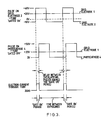
- Fig 3 The action of the voltage pulses in gating the image tube on and off can be seen by reference to Fig 3.
- typical operating potentials are indicated including a 50V amplitude for the applied voltage pulses.
- Fig 1 illustrates the streaking or framing image tube diagrammatically. All potentials are specified relative to photocathode 4.
- the image tube components are incorporated into a vacuum envelope 9.
- the photocathode 4 is formed on the inside surface of the glass faceplate 11 whilst a semi-transparent conducting electrode 10 is deposited on the outer surface of the faceplate 11 and connected electrically to photocathode 4 to ensure that capacitative charging effects within the glass faceplate are avoided during gating of the photocathode 4.
- First, second and third "grid" electrodes, 1, 2 and 3, preferably in the form of meshes, are arranged so that electrons from the photocathode must transverse all three electrodes on their passage down the tube. Included in the tube is a focus electrode 5 and anode 6.
- the image tube would normally include deflector plates 7 and 8 as shown.
- the tube also includes a phosphor screen 12.
- the tube may be of the construction as described in GB-PS-1458399.
- Fig 1 Potentials shown in Fig 1 are typical for the correct focussing of the tube although exact values will depend on the particular design of tube used.
- the potentials applied to grid electrodes 1 and 2 be kept to a minimum to ease the requirements of the gating circuitry. Also, to ensure that disturbance to the focus conditions is minimised the grid electrodes 1 and 2 should be operated at the equipotential values corresponding to the field between the photocathode 4 and grid electrode 3. Both above requirements militate for grid electrodes 1 and 2 being close spaced to the photocathode 4 with their construction being of fine mesh wire with a high transmission for electrons.
- the grids may be geometrically arranged to form a transmission line structure to ease high speed electronic operation.
- the mesh of the grid electrodes 1, 2 and 3 are of 1000 mesh/inch with a transmission for electrons of greater than 70%.
Landscapes
- Image-Pickup Tubes, Image-Amplification Tubes, And Storage Tubes (AREA)
Applications Claiming Priority (2)
| Application Number | Priority Date | Filing Date | Title |
|---|---|---|---|
| GB8725856 | 1987-11-04 | ||
| GB8725856A GB2211983B (en) | 1987-11-04 | 1987-11-04 | Improvements in or relating to a streaking or framing image tube |
Publications (3)
| Publication Number | Publication Date |
|---|---|
| EP0315435A2 true EP0315435A2 (de) | 1989-05-10 |
| EP0315435A3 EP0315435A3 (en) | 1989-11-23 |
| EP0315435B1 EP0315435B1 (de) | 1993-10-06 |
Family
ID=10626438
Family Applications (1)
| Application Number | Title | Priority Date | Filing Date |
|---|---|---|---|
| EP88310317A Expired - Lifetime EP0315435B1 (de) | 1987-11-04 | 1988-11-02 | Bildwandlerröhre zur Aufnahme von mit hoher Geschwindigkeit ablaufenden Vorgängen |
Country Status (5)
| Country | Link |
|---|---|
| US (1) | US4926039A (de) |
| EP (1) | EP0315435B1 (de) |
| JP (1) | JP2870768B2 (de) |
| DE (2) | DE315435T1 (de) |
| GB (1) | GB2211983B (de) |
Cited By (5)
| Publication number | Priority date | Publication date | Assignee | Title |
|---|---|---|---|---|
| JPH0367447A (ja) * | 1989-08-04 | 1991-03-22 | Hamamatsu Photonics Kk | 電子管ゲート方法及び電子管 |
| EP0474502A1 (de) * | 1990-09-07 | 1992-03-11 | Hamamatsu Photonics K.K. | Streakkamera mit einer Einrichtung zur Unterdrückung der Laufzeitunterschiede von Photoelektronen |
| EP0568376A1 (de) * | 1992-04-30 | 1993-11-03 | Hamamatsu Photonics K.K. | Bildaufnahmevorrichtung |
| EP0701185B1 (de) * | 1994-09-07 | 1998-05-13 | Imco Electro-Optics Limited | Verfahren und Vorrichtung für Hochgeschwindigkeitsbildaufnahme |
| CN100533648C (zh) * | 2005-12-30 | 2009-08-26 | 中国科学院西安光学精密机械研究所 | 一种静电聚焦飞秒条纹变相管 |
Families Citing this family (6)
| Publication number | Priority date | Publication date | Assignee | Title |
|---|---|---|---|---|
| NL8801671A (nl) * | 1988-07-01 | 1990-02-01 | Optische Ind De Oude Delft Nv | Werkwijze voor het bedrijven van een van een kanalenplaat voorziene beeldversterkerbuis en beeldversterkerbuisinrichting voorzien van een kanalenplaat. |
| US5336881A (en) * | 1993-03-01 | 1994-08-09 | Itt Corporation | High light resolution control of an image intensifier tube |
| GB2333642A (en) | 1998-01-21 | 1999-07-28 | Ibm | Photo-cathode electron source having an extractor grid |
| US6690098B1 (en) * | 2000-01-31 | 2004-02-10 | Litton Systems, Inc. | Method and system for gating a power supply in a radiation detector |
| GB2493532B (en) * | 2011-08-09 | 2016-03-09 | Invisible Vision Ltd | High speed high resolution electro-optic imaging |
| US9184032B1 (en) * | 2013-03-06 | 2015-11-10 | Exelis, Inc. | Performance regulated image intensifier power supply |
Family Cites Families (7)
| Publication number | Priority date | Publication date | Assignee | Title |
|---|---|---|---|---|
| BE791169A (fr) * | 1971-11-12 | 1973-05-09 | Westinghouse Electric Corp | Declencheur d'impulsions radiometriques a semi-conducteurs poursysteme de lecture d'appareils de mesure situes a distance |
| US3733492A (en) * | 1972-04-03 | 1973-05-15 | Machlett Lab Inc | Gateable image intensifier tube |
| GB1458399A (en) * | 1974-08-03 | 1976-12-15 | English Electric Valve Co Ltd | Electron optical image tubes |
| GB8505012D0 (en) * | 1985-02-27 | 1985-03-27 | Hadland Photonics Lts | Gating image tubes |
| JPS61250944A (ja) * | 1985-04-30 | 1986-11-08 | Toshiba Corp | X線イメ−ジインテンシフアイヤ |
| JPS62142235A (ja) * | 1985-12-16 | 1987-06-25 | Hamamatsu Photonics Kk | ストリ−クカメラ装置 |
| JPS62188915A (ja) * | 1986-02-14 | 1987-08-18 | Hamamatsu Photonics Kk | 2重掃引ストリ−クカメラ装置 |
-
1987
- 1987-11-04 GB GB8725856A patent/GB2211983B/en not_active Expired - Fee Related
-
1988
- 1988-11-02 DE DE198888310317T patent/DE315435T1/de active Pending
- 1988-11-02 DE DE88310317T patent/DE3884750T2/de not_active Expired - Fee Related
- 1988-11-02 EP EP88310317A patent/EP0315435B1/de not_active Expired - Lifetime
- 1988-11-02 US US07/266,411 patent/US4926039A/en not_active Expired - Lifetime
- 1988-11-04 JP JP63280242A patent/JP2870768B2/ja not_active Expired - Lifetime
Cited By (7)
| Publication number | Priority date | Publication date | Assignee | Title |
|---|---|---|---|---|
| JPH0367447A (ja) * | 1989-08-04 | 1991-03-22 | Hamamatsu Photonics Kk | 電子管ゲート方法及び電子管 |
| EP0474502A1 (de) * | 1990-09-07 | 1992-03-11 | Hamamatsu Photonics K.K. | Streakkamera mit einer Einrichtung zur Unterdrückung der Laufzeitunterschiede von Photoelektronen |
| US5221836A (en) * | 1990-09-07 | 1993-06-22 | Hamamatsu Photonics K.K. | Streak tube having an arrangement for suppressing travel time spread of photoelectrons |
| EP0568376A1 (de) * | 1992-04-30 | 1993-11-03 | Hamamatsu Photonics K.K. | Bildaufnahmevorrichtung |
| US5393972A (en) * | 1992-04-30 | 1995-02-28 | Hamamatsu Photonics K.K. | Imaging device with high speed shuttering |
| EP0701185B1 (de) * | 1994-09-07 | 1998-05-13 | Imco Electro-Optics Limited | Verfahren und Vorrichtung für Hochgeschwindigkeitsbildaufnahme |
| CN100533648C (zh) * | 2005-12-30 | 2009-08-26 | 中国科学院西安光学精密机械研究所 | 一种静电聚焦飞秒条纹变相管 |
Also Published As
| Publication number | Publication date |
|---|---|
| EP0315435A3 (en) | 1989-11-23 |
| EP0315435B1 (de) | 1993-10-06 |
| GB8725856D0 (en) | 1987-12-09 |
| JPH01289056A (ja) | 1989-11-21 |
| GB2211983A (en) | 1989-07-12 |
| US4926039A (en) | 1990-05-15 |
| JP2870768B2 (ja) | 1999-03-17 |
| GB2211983B (en) | 1992-03-18 |
| DE3884750D1 (de) | 1993-11-11 |
| DE315435T1 (de) | 1989-10-26 |
| DE3884750T2 (de) | 1994-02-10 |
Similar Documents
| Publication | Publication Date | Title |
|---|---|---|
| EP0315435B1 (de) | Bildwandlerröhre zur Aufnahme von mit hoher Geschwindigkeit ablaufenden Vorgängen | |
| US3710173A (en) | Direct viewing storage tube having mesh halftone target and nonmesh bistable target | |
| US2877376A (en) | Phosphor screen device | |
| US2259506A (en) | Cathode ray tube oscillograph | |
| US4694346A (en) | Method and apparatus for gating image tubes | |
| US2377972A (en) | Television transmitting system | |
| DE1439929B2 (de) | Verfahren zum elektronischen speichern verstaerken und ablesen von bildmaessig verteilten informationen | |
| JP2572388B2 (ja) | ストリ−ク管 | |
| US4216407A (en) | Flat panel display device with beam collector | |
| US3277334A (en) | Charge storage tube and target electrode therefor | |
| US4139800A (en) | Bistable storage target having interdigitated target electrode for selective erasure | |
| EP0123348A1 (de) | Farbanzeigevorrichtung | |
| CA1091747A (en) | Charge image charge transfer cathode ray tube having a scan expansion electron lens system and collimation electrode means | |
| US2885595A (en) | Cathode ray tubes | |
| CN100399496C (zh) | 一种场致发射显示板及其驱动方法 | |
| GB2031219A (en) | Crt matrix display | |
| JP2984013B2 (ja) | 陰極構体 | |
| US2135149A (en) | Image dissector and method of electron beam analysis | |
| DE901659C (de) | Fernsehbildzerlegerroehre | |
| KR840002156A (ko) | 촬상관 전자총 | |
| JPH0447886Y2 (de) | ||
| US3281622A (en) | Scan conversion tube wherein the flood beam passes through the storage electrode and is scanned over an image dissector | |
| US3838309A (en) | Direct view storage tube having a lateral field neutralizing electrode adjacent the storage grid | |
| JPH0778565A (ja) | 陰極線管の耐電圧処理方法 | |
| EP0183259A2 (de) | Bildröhrenschaltung |
Legal Events
| Date | Code | Title | Description |
|---|---|---|---|
| PUAI | Public reference made under article 153(3) epc to a published international application that has entered the european phase |
Free format text: ORIGINAL CODE: 0009012 |
|
| AK | Designated contracting states |
Kind code of ref document: A2 Designated state(s): CH DE FR GB LI NL |
|
| EL | Fr: translation of claims filed | ||
| PUAL | Search report despatched |
Free format text: ORIGINAL CODE: 0009013 |
|
| TCNL | Nl: translation of patent claims filed | ||
| DET | De: translation of patent claims | ||
| AK | Designated contracting states |
Kind code of ref document: A3 Designated state(s): CH DE FR GB LI NL |
|
| 17P | Request for examination filed |
Effective date: 19900530 |
|
| 17Q | First examination report despatched |
Effective date: 19930216 |
|
| GRAA | (expected) grant |
Free format text: ORIGINAL CODE: 0009210 |
|
| AK | Designated contracting states |
Kind code of ref document: B1 Designated state(s): CH DE FR GB LI NL |
|
| REF | Corresponds to: |
Ref document number: 3884750 Country of ref document: DE Date of ref document: 19931111 |
|
| ET | Fr: translation filed | ||
| PLBE | No opposition filed within time limit |
Free format text: ORIGINAL CODE: 0009261 |
|
| STAA | Information on the status of an ep patent application or granted ep patent |
Free format text: STATUS: NO OPPOSITION FILED WITHIN TIME LIMIT |
|
| 26N | No opposition filed | ||
| PGFP | Annual fee paid to national office [announced via postgrant information from national office to epo] |
Ref country code: CH Payment date: 19961121 Year of fee payment: 9 |
|
| PG25 | Lapsed in a contracting state [announced via postgrant information from national office to epo] |
Ref country code: LI Free format text: LAPSE BECAUSE OF NON-PAYMENT OF DUE FEES Effective date: 19971130 Ref country code: CH Free format text: LAPSE BECAUSE OF NON-PAYMENT OF DUE FEES Effective date: 19971130 |
|
| REG | Reference to a national code |
Ref country code: CH Ref legal event code: PL |
|
| REG | Reference to a national code |
Ref country code: GB Ref legal event code: IF02 |
|
| PGFP | Annual fee paid to national office [announced via postgrant information from national office to epo] |
Ref country code: DE Payment date: 20021107 Year of fee payment: 15 |
|
| PGFP | Annual fee paid to national office [announced via postgrant information from national office to epo] |
Ref country code: NL Payment date: 20021129 Year of fee payment: 15 |
|
| REG | Reference to a national code |
Ref country code: GB Ref legal event code: 732E |
|
| NLS | Nl: assignments of ep-patents |
Owner name: DRS HADLAND LTD. |
|
| REG | Reference to a national code |
Ref country code: FR Ref legal event code: TP |
|
| PG25 | Lapsed in a contracting state [announced via postgrant information from national office to epo] |
Ref country code: NL Free format text: LAPSE BECAUSE OF NON-PAYMENT OF DUE FEES Effective date: 20040601 |
|
| PG25 | Lapsed in a contracting state [announced via postgrant information from national office to epo] |
Ref country code: DE Free format text: LAPSE BECAUSE OF NON-PAYMENT OF DUE FEES Effective date: 20040602 |
|
| NLV4 | Nl: lapsed or anulled due to non-payment of the annual fee |
Effective date: 20040601 |
|
| REG | Reference to a national code |
Ref country code: GB Ref legal event code: 732E |
|
| REG | Reference to a national code |
Ref country code: FR Ref legal event code: TP |
|
| REG | Reference to a national code |
Ref country code: GB Ref legal event code: 732E |
|
| PGFP | Annual fee paid to national office [announced via postgrant information from national office to epo] |
Ref country code: GB Payment date: 20071031 Year of fee payment: 20 Ref country code: FR Payment date: 20071108 Year of fee payment: 20 |
|
| REG | Reference to a national code |
Ref country code: GB Ref legal event code: PE20 Expiry date: 20081101 |
|
| REG | Reference to a national code |
Ref country code: FR Ref legal event code: TP Ref country code: FR Ref legal event code: CD |
|
| PG25 | Lapsed in a contracting state [announced via postgrant information from national office to epo] |
Ref country code: GB Free format text: LAPSE BECAUSE OF EXPIRATION OF PROTECTION Effective date: 20081101 |