EP0313097A2 - Microcomputer system including master processor and slave processor - Google Patents
Microcomputer system including master processor and slave processor Download PDFInfo
- Publication number
- EP0313097A2 EP0313097A2 EP88117683A EP88117683A EP0313097A2 EP 0313097 A2 EP0313097 A2 EP 0313097A2 EP 88117683 A EP88117683 A EP 88117683A EP 88117683 A EP88117683 A EP 88117683A EP 0313097 A2 EP0313097 A2 EP 0313097A2
- Authority
- EP
- European Patent Office
- Prior art keywords
- signal
- level
- coprocessor
- master processor
- processor
- Prior art date
- Legal status (The legal status is an assumption and is not a legal conclusion. Google has not performed a legal analysis and makes no representation as to the accuracy of the status listed.)
- Granted
Links
Images


Classifications
-
- G—PHYSICS
- G06—COMPUTING; CALCULATING OR COUNTING
- G06F—ELECTRIC DIGITAL DATA PROCESSING
- G06F9/00—Arrangements for program control, e.g. control units
- G06F9/06—Arrangements for program control, e.g. control units using stored programs, i.e. using an internal store of processing equipment to receive or retain programs
- G06F9/30—Arrangements for executing machine instructions, e.g. instruction decode
- G06F9/38—Concurrent instruction execution, e.g. pipeline, look ahead
- G06F9/3877—Concurrent instruction execution, e.g. pipeline, look ahead using a slave processor, e.g. coprocessor
Definitions
- the present invention relates to a microcomputer system and, more particularly, to a microcomputer system wherein a master processor and at least one coprocessor are interconnected via a bus.
- a microprocessor In a microprocessor fabricated on a single semiconductor chip, a very large number of circuit elements are required but the number of circuit elements capable of being formed in the single chip is limited. Therefore, it is difficult to fabricate such a unit in a single chip that executes high level instructions such as a floating-point arithmetic operation, a function arithmetic operation, etc., at a high speed.
- a coprocessor is employed, which executes the high level instructions in place of the microprocessor.
- the coprocessor operates under the control of the microprocessor and is thus called a "slave processor".
- the microprocessor operates by itself as a central processing unit (CPU) to control the coprocessor along with a memory and peripheral units and is thus called a "master processor".
- CPU central processing unit
- the master processor When the master processor decodes the high level instruction, it makes access to the slave processor to transfer the high level instruction as well as one or more operands, if necessary. The slave processor is thereby brought into an operative condition to execute the high level instruction thus supplied. If the master processor is not connected with slave processor, it should execute the high level instructions by use of its own arithmetic unit. Therefore, the master processor is required to detect whether or not the slave processor is connected thereto. In a case of provision of the slave processor, moreover, if the arithmetic exception occurs in the arithmetic result or arithmetic procedure of the slave processor, the master processor should perform the processing operation for the arithmetic exception occurring in the slave processor. Therefore, the master processor is further required to detect whether or not the status information of the slave processor is necessary to be read therefrom.
- the master processor includes first and second terminals supplied respectively with a busy signal and a status read request signal from the slave processor, as disclosed in the above copending application.
- the slave processor changes the busy signal from an inactive level to an active level and holds the active level of the busy signal during the executing period thereof.
- the slave processor completes the execution of the high level instruction, it changes the busy signal from the active level to the inactive level.
- the slave processor produces an inactive level of the status read request signal when it changes the busy signal from the active level to the inactive level.
- the slave processor produces an active level of the status read request signal.
- the master processor detects the level of the first terminal, i.e. the level of the busy signal, and further detects the level of the status read request signal supplied to the second terminal when the busy signal is in the inactive level.
- both the first and second terminals of the master processor i.e. both the busy signal and status read request signal, are maintained to the inactive level and the active level, respectively.
- the status read request signal is in the inactive level when the busy signal is changed from the active level to the inactive level.
- the master processor can detect whether or not the slave processor is connected thereto and whether or not the arithmetic exception occurs in the slave processor.
- the high level instructions to be executed by the slave processor are divided into two types: the first type of instructions is such that the execution result is required to be returned to the master processor and the second type of instructions is such that the execution result is not required to be returned to the master processor and is stored into, for example, a register of the slave processor.
- the first type instruction is read from an instruction memory
- the master processor must wait for the completion of the execution of this type instruction by the slave processor.
- the slave processor executes the second type high level instruction
- the master processor can execute subsequent low level instructions in parallel to the execution of the second type instruction by the slave processor.
- the master processor does not require the execution result of the second type high level instruction, it shoud detect whether or not the arithmetic exception occurs in the slave processor and, if occurs, read the status information to detect the kind of the arithmetic exception. To this end, the master processor always detects the levels at the first and second terminals, i.e. the levels of the busy signal and the status read request signal, after transferring the high level instruction irrespective of the types of the high level instruction which is now to be executed by the slave processor.
- the slave processor When the slave processor receives a new high level instruction, if the arithmetic exception has occurred in the execution result or the executing procedure of the precedingly supplied second type instruction, the slave processor changes the busy signal to the active level and immediately returns it to the inactive level with holding the status read request signal at the active level. In a case where the arithmetic exception has not occurs, the slave processor changes the busy signal to the active level and after changing the status read request signal to the inactive level, returns the busy signal to the inactive level.
- the master processor can detect whether or not the arithmetic exception has occurs in the execution of the second type high level instruction by the slave processor.
- the master processor since the master processor detects the levels of the first and second terminals whenever the high level instruction is decoded, it is delayed to start execution of subsequent low level instructions when a new one of the second type high level instructions is decoded and when the arithmetic exception has not occurred in the execution of the preceding one of second type high level instructions.
- a primary object of the present invention is to provide an improved microcomputer system in which a master processor and at least one slave processor are interconnected via a bus.
- Another object of the present invention is to provide a microcomputer system in which a master processor can execute at least one low level instruction in parallel to the execution of a high level instruction by a slave processor without delaying the starting time of the execution of the low level instruction.
- Still another object of the present invention is to provide an improved master processor or a microprocessor capable of being connected with at least one coprocessor and executing at least one instruction while the coprocessor is executing another instruction.
- a microcomputer system comprises a master processor, a coprocessor, and a bus interconnecting the master processor and the coprocessor, and the master processor includes first, second and third terminals supplied respectively with first, second and third signals from the coprocessor.
- the first signal corresponds to the above-mentioned busy signal and thus takes an active level when the master processor is required to be in a wait condition
- the second signal corresponds to the above-mentioned status read request signal and thus takes an active level at least when the first signal is changed from the active level to an inactive level in a state of occurrence of arithmetic exception.
- the third signal is provided in accordance with the present invention and takes an active level when the coprocessor is not be executing an instruction and when arithmetic exception does not occur in the execution of a preceding instruction.
- the master processor further includes means coupled to the third terminal for detecting the level of the third signal, means responsive to a first output of the detecting means representative of the active level of the third signal for executing at least one instruction in parallel to the execution of the coprocessor irrespective of the levels of the first and second terminals, and means responsive to a second output of the detecting means representative of the inactive level of the third signal for bringing the master processor into the wait condition until the first signal is changed to the inactive level and for performing a subsequent processing operation responsive to the second signal after the first signal is changed to the inactive level.
- the master processor can start the execution of at least one subsequent instruction in parallel to the execution of that second type high level instruction by the coprocessor without being brought into the wait condition by the first signal.
- the executing start timing of the subsequent instruction is thereby fastened.
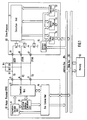
- a microcomputer system includes a master processor 101 as a CPU, a slave processor 102 as a coprocessor and a memory 103 which are interconnected via an address bus 104 and a data Bus 105.
- the slave processor 102 operates under the control of the master processor 101 and executes at a high speed high level instructions such as a floating-point arithmetic operation, a function arithmetic operation, etc., in place of the master processor 101.
- the memory 103 stores data and a program including low level instructions and high level instructions and is made access by the master processor 101.
- the master processor 101 includes an instruction decoder unit 11 decoding instructions which are executed by the master and slave processors 101 and 102, an execution unit 12 controlling the whole operation of the master processor 101 and executing the low level instructions under the sequential control of a microprogram, an effective address calculation unit 13 calculating an effective address of each operand for the respective instructions, and a bus control unit 14 controlling the address and data buses 104 and 105 to make access to the memory 103 and the slave processor 102. These units 11 to 14 are coupled as shown via internal buses.
- the master processor 101 further includes a first input terminal 15 supplied with a BUSY signal, a second input terminal 16 supplied with a CPERR signal and a third input terminal 17 supplied with a CPEND signal, the third input terminal 17 being provided in accordance with the present invention.
- the slave processor 102 includes an execution unit 31 performing an arithmetic operation responsive to each of the high level instructions, a command port 32 receiving and temporarily storing command code (opecodes) of each instruction transferred via the data bus 105, a status port 33 temporarily storing the status information supplied from the execution unit 31 and outputting it onto the data bus 105, an operand port 34 temporarily storing one or more operands transferred via the data bus 105 for the arithmetic operation of the unit 31 and receiving and outputting the execution result from the unit 31 onto the data bus 105, if necessary.
- the slave processor 102 also includes and address decoder 35 decoding address information supplied via the address bus 104 and selecting one of the units 32, 33 and 34 in response thereto to write or read data into or from the selected unit.
- the slave processor 102 further includes three output terminals 39, 40 and 41 and three transistors 36, 37 and 38 of an open-drain type. Each of the transistors 36, 37 and 38 has a drain-source path connected between each of the terminals 39, 40 and 41 and a ground point and a gate connected the execution unit 31.
- the terminal 41 and transistor 38 are provided in accordance with the present invention.
- the output terminals 39, 40 and 41 of the slave processor 102 are connected to the input terminals 15, 16 and 17 of the master processor 101 via signal lines 111, 112 and 113, respectively, which lines are in turn pulled up to a power voltage via resistors 61, 62 and 63, respectively. Accordingly, so long as the transistors 36 to 38 are in the nonconductive state, the BUSY, CPERR and CPEND signals, i.e. the input terminals 15 to 16 of the master processor 101, are maintained at the high level.
- the execution unit 31 of the slave processor 102 turns the transistor 36 ON to change the BUSY signal to an active level (low level in this embodiment) unit the execution of the receiving instruction is completed.
- the execution unit 31 thereof turns the transistor 36 ON and immediately thereafter turns it OFF. Accordingly, the BUSY signal is changed to the low level and immediated returned to the high level.
- the execution unit 31 remains the transistor 36 in the conductive level to produce the low level BUSY signal until the completion of the execution of the current second type instruction.
- the execution unit 31 of the slave processor 102 turns the transistor 37 ON with changing the transistor 36 from the conductive state to the nonconductive state, when 110 arithmetic exception occurs in the execution result or the executing procedure of the high level instruction.
- the CPERR signal thereby takes an inactive level (the high level).
- the transistor 37 is held in the non conductive state to produce an active level (the high level) of the CPERR signal.
- the execution unit 31 of the slave processor 102 turns the transistor 38 ON during the executing period of the high level instruction, and when the arithmetic exception occurs, it remains the transistor 38 in the conductive state unit the master processor 101 reads from the status port 34 the status information representative of the arithmetic exception.
- the slave processor 102 is free of the executing state of the high level instruction and when it stores no arithmetic exception, the transistor 38 is in the nonconductive state.
- the CPEND signal thereby takes an active level (the high level). Since the active and inactive levels of the BUSY, CPERR and CPEND signals are determined as described above, the master processor 101 can judge the operating state of the slave processor 102 by detecting the levels of the input terminals 15, 16 and 17.
- a protocol operating procedure between the master and slave processors 101 and 102 is activated in accordance with the microprogram stored in execution unit 12.
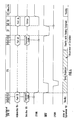
- This procedure is shown in Fig. 2 as a flow chart.
- the read-out instruction denotes a dyadic operation on two operands stored in the memory 103
- the execution unit 12 prompts the bus control unit 14 to read these operands from the memory 14 and to transfer them to the operand port 33 of the slave processor 102.
- the bus control unit 14 controls the address and data buses 104 and 105 to writes the operands into the operand port 33 (step 200).
- step 200 is not carried out. Thereafter, the command code (opecode) of the high level instruction is transferred to the command port 32 of the slave processor 102 via the data bus 105 under the control of the bus control unit 14 (step 201). In a subsequent step 202, it is judged which type instruction is transferred. Assuming that the instruction to be transferred or executed is the second type instruction representing that the execution result is not required to be returned to the master processor 101, a step 211 is performed.
- the execution unit 12 of the master processor 101 detects the level of the terminal 17, i.e. the CPEND signal, not detects the levels of the terminals 15 and 16, i.e. the BUSY and CPERR signals, in accordance with the present invention.
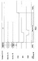
- the CPEND signal i.e. the terminal 17, takes the active level (high level), as shown in Fig. 3.
- the master processor 101 waits for the completion of the bus cycle for transferring the command code to the command port 32 (step 212) and then reads and executes the subsequent instructions (step 213). That is, the master processor 101 executes the subsequent instructions in parallel to the execution of the second type high level instruction by the slave processor 102, as shown in Fig. 3. Since the level of the BUSY signal is not detected, the active level thereof is ignored.
- the slave processor 102 completes the execution of the instruction without occurrence of the arithmetic exception, it stores the execution result into the internal register thereof and turns the transistor 38 OFF to produce the active level of the CPEND signal, as shown in Fig. 3.
- the execution unit 31 of the slave processor 102 maintains the transistor 38 in the conductive state to produce the inactive level (low level) of the CPEND signal, as shown in Fig. 4.
- the unit 31 further writes into the status port 34 the status information representative of the arithmetic exception.
- the master processor 101 performs the steps 200, 201, 202 and 211, but the CPEND signal takes the inactive level, so that the operating procedure shifts to a step 203.
- the master processor 101 waits for the completion of writing the command code of that subsequent second type high level instruction into the command port 32.
- the execution unit 31 turns the transistor 36 ON and immediately thereafter turns it OFF. Since the status port 34 stores the information representative of the exception, the unit 31 turns the transistor 36 OFF with remaining the transistor 37 in the nonconductive state to produce the active level of the CPERR signal, as shown in Fig. 4.
- the master processor 101 is brought into a wait condition until the BUSY signal takes the inactive level (step 204) and thereafter it detects the level of the CPERR signal (step 205).
- the master processor 101 Since the CPERR signal is at the active level, the master processor 101 reads the status information out of the status port 34 of the slave processor 102 (step 206), as shown in Fig. 4. The read-out status information is judged in a step 207, and in accordance with the value thereof, the master processor 102 performs an processing operation for the arithmetic exception (step 208) or an processing operation for the slave processor absence exception (step 209). Since the exception information stored in the port 34 has been read out, the execution unit 31 turns the transistor 38 OFF to produce the active level of the CPEND signal. During the processing operation for the exception by the master processor 101, the slave processor 102 is brought into the standby condition. After the completion of the processing operation for the exception, the master processor 101 restarts to execute the program from the suspended address.
- a subsequent second type high level instruction 2 is read from the memory 103 while the slave processor 102 is executing the preceding second type high level instruction 1.
- the master processor 101 performs the steps 200,201 and 202 and advances to the step 211. Since the slave processor 102 is yet in the executing state of the instruction, the CPEND signal takes the inactive level, as shown in Fig. 5. Therefore, the master processor 104 waits for the end of the bus cycle (step 203) and detects the level of the BUSY signal.
- the slave processor 102 turns the transistor 36 ON, and in this case the execution unit 31 is in the executing state of the instruction 1, so that the transistor 36 is held in the conductive state to maintain the active level of BUSY signal unit the execution of instruction1 is completed, as shown in Fig. 5.
- the master processor 101 is brought into the wait condition (step 204).
- the execution unit 31 turns the transistor 36 OFF with turning the transistor 37 ON.
- the execution unit further starts to execute the instruction2, so that the transistor 38 is held in the conductive state.
- the master processor 101 In response to the change of the BUSY signal to the inactive level, on the other hand, the master processor 101 detects the inactive level of the CPERR signal (step 205). It should be noted that the instruction 1 is the second type instruction. Therefore, the master processor 101 executes the subsequent instructions (step 213).
- the master processor 101 When the first type high level instruction is read from the memory 103 and decoded by the unit 11, the master processor 101 performs the steps 200, 201, 202 and 203. The step 211 is not performed and the CPEND signal is ignored. On the other hand, the slave processor 102 maintains the BUSY signal at the active level until completion of this first type instruction, as shown in Fig. 6. During this period, the master processor 101 is brought into the wait condition (step 204). When the execution of the first type instruction is completed without occurrence of the arithmetic exception, the slave processor 102 changes the BUSY signal to the inactive level with producing the inactive level of the CPERR signal, as shown in Fig. 6. The slave processor 102 further writes the execution result into the operand port 33 thereof. The master processor 101 responds to the inactive level of the CPERR signal (step 205) and makes access to the operand port 33 to read the execution result therefrom (step 209).
- the slave processor 104 changes the BUSY signal to the inactive level with mainting the active level of the CPERR signal, as shown in Fig. 7. Accordingly, the master processor 101 makes access to the status port 34 to read the status information therefrom (step 206), judges the status (step 207) and performs the processing operation for the exception (step 208 or 210), as shown in Fig. 7.
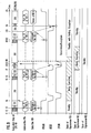
- a microcomputer system includes three slave processors (coprocessors) 102-1, 102-2 and 102-3.
- the same constituents as those shown in Fig. 1 are denoted by the same reference numerals to omit further description thereof.
- Each of the slave processors 102-1, 102-2 and 102-3 drives the signal lines 111, 112 and 113 by use of open-drain transistors. Accordingly, when any one of the slave processors 102-1, 102-2 and 102-3 drives the signal lines 111, 112 and 113 to the low level, the master processor 101 receives the low levels of the BUSY, CPERR and CPEND signals.
- the master processor 101 waits for the completion of the bus cycle (at a time point t7) and detects the levels of the BUSY and CPERR signals (at time points t8 and t9). Since the second type instruction is transferred to the second slave processor 102-2, the master processor 101 starts to executes subsequent instructions at the time point t9.
- the master processor 101 makes again access to the first slave processor 102 to transfer the first or second type instruction.
- the master processor 101 detects the inactive level of the CPEND signal at a time point t12, so that it waits for the completion of the bus cycle (a time point t13) and for the change of the BUSY signal to the inactive level (a time point t14).
- the master processor 101 Since the first slave processor 102-1 holds the arithmetic exception, it changes the BUSY signal to the inactive level with holding the active level of the CPERR signal (a time point t14). Therefore, the master processor 101 reads the exception status information from the status port of the first slave processor 102-1 and performs the processing operation for the exception.
Landscapes
- Engineering & Computer Science (AREA)
- Software Systems (AREA)
- Theoretical Computer Science (AREA)
- Physics & Mathematics (AREA)
- General Engineering & Computer Science (AREA)
- General Physics & Mathematics (AREA)
- Advance Control (AREA)
- Multi Processors (AREA)
Abstract
Description
- This application is related to the following copending application:
- Ser. No. 119,601, filed by the same assignee for Takashi Nakayama on Nov. 12, 1987, under a title of "Micro Processor Capable of Being Connected with Coprocessor".
- The present invention relates to a microcomputer system and, more particularly, to a microcomputer system wherein a master processor and at least one coprocessor are interconnected via a bus.
- In a microprocessor fabricated on a single semiconductor chip, a very large number of circuit elements are required but the number of circuit elements capable of being formed in the single chip is limited. Therefore, it is difficult to fabricate such a unit in a single chip that executes high level instructions such as a floating-point arithmetic operation, a function arithmetic operation, etc., at a high speed. In order to solve this problem, a coprocessor is employed, which executes the high level instructions in place of the microprocessor. The coprocessor operates under the control of the microprocessor and is thus called a "slave processor". The microprocessor operates by itself as a central processing unit (CPU) to control the coprocessor along with a memory and peripheral units and is thus called a "master processor".
- When the master processor decodes the high level instruction, it makes access to the slave processor to transfer the high level instruction as well as one or more operands, if necessary. The slave processor is thereby brought into an operative condition to execute the high level instruction thus supplied. If the master processor is not connected with slave processor, it should execute the high level instructions by use of its own arithmetic unit. Therefore, the master processor is required to detect whether or not the slave processor is connected thereto. In a case of provision of the slave processor, moreover, if the arithmetic exception occurs in the arithmetic result or arithmetic procedure of the slave processor, the master processor should perform the processing operation for the arithmetic exception occurring in the slave processor. Therefore, the master processor is further required to detect whether or not the status information of the slave processor is necessary to be read therefrom.
- For these purposes, the master processor includes first and second terminals supplied respectively with a busy signal and a status read request signal from the slave processor, as disclosed in the above copending application. When the master processor decodes and transfers the high level instruction to the slave processor, the slave processor changes the busy signal from an inactive level to an active level and holds the active level of the busy signal during the executing period thereof. When the slave processor completes the execution of the high level instruction, it changes the busy signal from the active level to the inactive level. At this time, in a case of no occurrence of the arithmetic exception, the slave processor produces an inactive level of the status read request signal when it changes the busy signal from the active level to the inactive level. In contrast, if the arithmetic exception occurs, the slave processor produces an active level of the status read request signal. On the other hand, the master processor detects the level of the first terminal, i.e. the level of the busy signal, and further detects the level of the status read request signal supplied to the second terminal when the busy signal is in the inactive level. Thus, if the slave processor is not provided, both the first and second terminals of the master processor, i.e. both the busy signal and status read request signal, are maintained to the inactive level and the active level, respectively. On the other hand, in cases of provision of the slave processor and no occurrence of the arithmetic exception, the status read request signal is in the inactive level when the busy signal is changed from the active level to the inactive level. As a result, the master processor can detect whether or not the slave processor is connected thereto and whether or not the arithmetic exception occurs in the slave processor.
- The high level instructions to be executed by the slave processor are divided into two types: the first type of instructions is such that the execution result is required to be returned to the master processor and the second type of instructions is such that the execution result is not required to be returned to the master processor and is stored into, for example, a register of the slave processor. When the first type instruction is read from an instruction memory, the master processor must wait for the completion of the execution of this type instruction by the slave processor. On the other hand, when the slave processor executes the second type high level instruction, the master processor can execute subsequent low level instructions in parallel to the execution of the second type instruction by the slave processor.
- Although the master processor does not require the execution result of the second type high level instruction, it shoud detect whether or not the arithmetic exception occurs in the slave processor and, if occurs, read the status information to detect the kind of the arithmetic exception. To this end, the master processor always detects the levels at the first and second terminals, i.e. the levels of the busy signal and the status read request signal, after transferring the high level instruction irrespective of the types of the high level instruction which is now to be executed by the slave processor. When the slave processor receives a new high level instruction, if the arithmetic exception has occurred in the execution result or the executing procedure of the precedingly supplied second type instruction, the slave processor changes the busy signal to the active level and immediately returns it to the inactive level with holding the status read request signal at the active level. In a case where the arithmetic exception has not occurs, the slave processor changes the busy signal to the active level and after changing the status read request signal to the inactive level, returns the busy signal to the inactive level. Thus, the master processor can detect whether or not the arithmetic exception has occurs in the execution of the second type high level instruction by the slave processor. However, since the master processor detects the levels of the first and second terminals whenever the high level instruction is decoded, it is delayed to start execution of subsequent low level instructions when a new one of the second type high level instructions is decoded and when the arithmetic exception has not occurred in the execution of the preceding one of second type high level instructions.
- Therefore, a primary object of the present invention is to provide an improved microcomputer system in which a master processor and at least one slave processor are interconnected via a bus.
- Another object of the present invention is to provide a microcomputer system in which a master processor can execute at least one low level instruction in parallel to the execution of a high level instruction by a slave processor without delaying the starting time of the execution of the low level instruction.
- Still another object of the present invention is to provide an improved master processor or a microprocessor capable of being connected with at least one coprocessor and executing at least one instruction while the coprocessor is executing another instruction.
- A microcomputer system according to the present invention comprises a master processor, a coprocessor, and a bus interconnecting the master processor and the coprocessor, and the master processor includes first, second and third terminals supplied respectively with first, second and third signals from the coprocessor. The first signal corresponds to the above-mentioned busy signal and thus takes an active level when the master processor is required to be in a wait condition, and the second signal corresponds to the above-mentioned status read request signal and thus takes an active level at least when the first signal is changed from the active level to an inactive level in a state of occurrence of arithmetic exception. The third signal is provided in accordance with the present invention and takes an active level when the coprocessor is not be executing an instruction and when arithmetic exception does not occur in the execution of a preceding instruction. The master processor further includes means coupled to the third terminal for detecting the level of the third signal, means responsive to a first output of the detecting means representative of the active level of the third signal for executing at least one instruction in parallel to the execution of the coprocessor irrespective of the levels of the first and second terminals, and means responsive to a second output of the detecting means representative of the inactive level of the third signal for bringing the master processor into the wait condition until the first signal is changed to the inactive level and for performing a subsequent processing operation responsive to the second signal after the first signal is changed to the inactive level.
- Thus, when the second type high level instruction is read out and the third signal takes the active level at this time, the master processor can start the execution of at least one subsequent instruction in parallel to the execution of that second type high level instruction by the coprocessor without being brought into the wait condition by the first signal. The executing start timing of the subsequent instruction is thereby fastened.
- The above and other objects, advantages and features of the present invention will be more apparent from the following description taken in conjunction with the accompany drawings, in which:
- Fig. 1 is a block diagram representative of an embodiment of the present invention;
- Fig. 2 is a flow chart representative of a sequence control procedure of a master processor shown in Fig. 1;
- Figs. 3, 4, 5, 6 and 7 are timing chart each representative of operations of a microcomputer system shown in Fig. 1;
- Fig. 8 is a block diagram representative of another embodiment of the present invention; and
- Fig. 9 is a timing chart representative of operations of a microcomputer system shown in Fig. 8.
- Referring to Fig. 1, a microcomputer system according to an embodiment of the present invention includes a
master processor 101 as a CPU, aslave processor 102 as a coprocessor and amemory 103 which are interconnected via anaddress bus 104 and adata Bus 105. Theslave processor 102 operates under the control of themaster processor 101 and executes at a high speed high level instructions such as a floating-point arithmetic operation, a function arithmetic operation, etc., in place of themaster processor 101. Thememory 103 stores data and a program including low level instructions and high level instructions and is made access by themaster processor 101. - The
master processor 101 includes aninstruction decoder unit 11 decoding instructions which are executed by the master andslave processors master processor 101 and executing the low level instructions under the sequential control of a microprogram, an effective address calculation unit 13 calculating an effective address of each operand for the respective instructions, and a bus control unit 14 controlling the address anddata buses memory 103 and theslave processor 102. Theseunits 11 to 14 are coupled as shown via internal buses. Themaster processor 101 further includes a first input terminal 15 supplied with a BUSY signal, asecond input terminal 16 supplied with a CPERR signal and athird input terminal 17 supplied with a CPEND signal, thethird input terminal 17 being provided in accordance with the present invention. - The
slave processor 102 includes an execution unit 31 performing an arithmetic operation responsive to each of the high level instructions, acommand port 32 receiving and temporarily storing command code (opecodes) of each instruction transferred via thedata bus 105, astatus port 33 temporarily storing the status information supplied from the execution unit 31 and outputting it onto thedata bus 105, anoperand port 34 temporarily storing one or more operands transferred via thedata bus 105 for the arithmetic operation of the unit 31 and receiving and outputting the execution result from the unit 31 onto thedata bus 105, if necessary. Theslave processor 102 also includes andaddress decoder 35 decoding address information supplied via theaddress bus 104 and selecting one of theunits slave processor 102 further includes threeoutput terminals transistors transistors terminals terminal 41 andtransistor 38 are provided in accordance with the present invention. - The
output terminals slave processor 102 are connected to theinput terminals master processor 101 viasignal lines resistors transistors 36 to 38 are in the nonconductive state, the BUSY, CPERR and CPEND signals, i.e. the input terminals 15 to 16 of themaster processor 101, are maintained at the high level. When theslave processor 102 receives the first type of the high level instruction representing that the execution result is required to be returned to themaster processor 101, the execution unit 31 of theslave processor 102 turns thetransistor 36 ON to change the BUSY signal to an active level (low level in this embodiment) unit the execution of the receiving instruction is completed. On the other hand, when theslave processor 102 receives the second type of the high level instruction representing that the execution result is not required to be returned to themaster processor 101, the execution unit 31 thereof turns thetransistor 36 ON and immediately thereafter turns it OFF. Accordingly, the BUSY signal is changed to the low level and immediated returned to the high level. However, when theslave processor 102 receives the subsequent second type instruction while it is executing the current second type instruction, the execution unit 31 remains thetransistor 36 in the conductive level to produce the low level BUSY signal until the completion of the execution of the current second type instruction. The execution unit 31 of theslave processor 102 turns the transistor 37 ON with changing thetransistor 36 from the conductive state to the nonconductive state, when 110 arithmetic exception occurs in the execution result or the executing procedure of the high level instruction. The CPERR signal thereby takes an inactive level (the high level). On the other hand, when the arithmetic exception occurs or when themaster processor 101 does not yet read from thestatus port 34 the status information representative of the arithmetic exception, the transistor 37 is held in the non conductive state to produce an active level (the high level) of the CPERR signal. The execution unit 31 of theslave processor 102 turns thetransistor 38 ON during the executing period of the high level instruction, and when the arithmetic exception occurs, it remains thetransistor 38 in the conductive state unit themaster processor 101 reads from thestatus port 34 the status information representative of the arithmetic exception. When theslave processor 102 is free of the executing state of the high level instruction and when it stores no arithmetic exception, thetransistor 38 is in the nonconductive state. The CPEND signal thereby takes an active level (the high level). Since the active and inactive levels of the BUSY, CPERR and CPEND signals are determined as described above, themaster processor 101 can judge the operating state of theslave processor 102 by detecting the levels of theinput terminals - When the high level instruction to be executed by the
slave processor 102 is read from thememory 103 and then decoded by theinstruction decoder unit 11 of themaster processor 101, a protocol operating procedure between the master andslave processors memory 103, the execution unit 12 prompts the bus control unit 14 to read these operands from the memory 14 and to transfer them to theoperand port 33 of theslave processor 102. Thus, the bus control unit 14 controls the address anddata buses slave processor 102, thestep 200 is not carried out. Thereafter, the command code (opecode) of the high level instruction is transferred to thecommand port 32 of theslave processor 102 via thedata bus 105 under the control of the bus control unit 14 (step 201). In asubsequent step 202, it is judged which type instruction is transferred. Assuming that the instruction to be transferred or executed is the second type instruction representing that the execution result is not required to be returned to themaster processor 101, astep 211 is performed. - In this
step 211, the execution unit 12 of themaster processor 101 detects the level of the terminal 17, i.e. the CPEND signal, not detects the levels of theterminals 15 and 16, i.e. the BUSY and CPERR signals, in accordance with the present invention. Assuming that theslave processor 102 is not in the executing state (i.e., in the standby state) and the arithmetic exception has not occurred in the execution of the preceding high level instruction, the CPEND signal, i.e. the terminal 17, takes the active level (high level), as shown in Fig. 3. Therefore, themaster processor 101 waits for the completion of the bus cycle for transferring the command code to the command port 32 (step 212) and then reads and executes the subsequent instructions (step 213). That is, themaster processor 101 executes the subsequent instructions in parallel to the execution of the second type high level instruction by theslave processor 102, as shown in Fig. 3. Since the level of the BUSY signal is not detected, the active level thereof is ignored. When theslave processor 102 completes the execution of the instruction without occurrence of the arithmetic exception, it stores the execution result into the internal register thereof and turns thetransistor 38 OFF to produce the active level of the CPEND signal, as shown in Fig. 3. - In contrast, when the arithmetic exception occurs in the execution of the second type instruction, the execution unit 31 of the
slave processor 102 maintains thetransistor 38 in the conductive state to produce the inactive level (low level) of the CPEND signal, as shown in Fig. 4. The unit 31 further writes into thestatus port 34 the status information representative of the arithmetic exception. In this condition, when a subsequent second type high level instruction is read out of the memory and decoded by theunit 11, themaster processor 101 performs thesteps step 203. In thisstep 203, themaster processor 101 waits for the completion of writing the command code of that subsequent second type high level instruction into thecommand port 32. In response thereto, the execution unit 31 turns thetransistor 36 ON and immediately thereafter turns it OFF. Since thestatus port 34 stores the information representative of the exception, the unit 31 turns thetransistor 36 OFF with remaining the transistor 37 in the nonconductive state to produce the active level of the CPERR signal, as shown in Fig. 4. On the other hand, themaster processor 101 is brought into a wait condition until the BUSY signal takes the inactive level (step 204) and thereafter it detects the level of the CPERR signal (step 205). Since the CPERR signal is at the active level, themaster processor 101 reads the status information out of thestatus port 34 of the slave processor 102 (step 206), as shown in Fig. 4. The read-out status information is judged in astep 207, and in accordance with the value thereof, themaster processor 102 performs an processing operation for the arithmetic exception (step 208) or an processing operation for the slave processor absence exception (step 209). Since the exception information stored in theport 34 has been read out, the execution unit 31 turns thetransistor 38 OFF to produce the active level of the CPEND signal. During the processing operation for the exception by themaster processor 101, theslave processor 102 is brought into the standby condition. After the completion of the processing operation for the exception, themaster processor 101 restarts to execute the program from the suspended address. - Assume now that, as shown in Fig. 5, a subsequent second type
high level instruction ② is read from thememory 103 while theslave processor 102 is executing the preceding second typehigh level instruction ①. In response to the reading-out of thesubsequent instruction ②, themaster processor 101 performs the steps 200,201 and 202 and advances to thestep 211. Since theslave processor 102 is yet in the executing state of the instruction, the CPEND signal takes the inactive level, as shown in Fig. 5. Therefore, themaster processor 104 waits for the end of the bus cycle (step 203) and detects the level of the BUSY signal. In response to a fact that the command code of thesubsequent instruction ② is written into thecommand port 32, theslave processor 102 turns thetransistor 36 ON, and in this case the execution unit 31 is in the executing state of theinstruction ①, so that thetransistor 36 is held in the conductive state to maintain the active level of BUSY signal unit the execution of instruction① is completed, as shown in Fig. 5. As a result, themaster processor 101 is brought into the wait condition (step 204). When the execution of theinstruction ① is completed without arithmetic exception, the execution unit 31 turns thetransistor 36 OFF with turning the transistor 37 ON. The execution unit further starts to execute the instruction②, so that thetransistor 38 is held in the conductive state. In response to the change of the BUSY signal to the inactive level, on the other hand, themaster processor 101 detects the inactive level of the CPERR signal (step 205). It should be noted that theinstruction ① is the second type instruction. Therefore, themaster processor 101 executes the subsequent instructions (step 213). - When the first type high level instruction is read from the
memory 103 and decoded by theunit 11, themaster processor 101 performs thesteps step 211 is not performed and the CPEND signal is ignored. On the other hand, theslave processor 102 maintains the BUSY signal at the active level until completion of this first type instruction, as shown in Fig. 6. During this period, themaster processor 101 is brought into the wait condition (step 204). When the execution of the first type instruction is completed without occurrence of the arithmetic exception, theslave processor 102 changes the BUSY signal to the inactive level with producing the inactive level of the CPERR signal, as shown in Fig. 6. Theslave processor 102 further writes the execution result into theoperand port 33 thereof. Themaster processor 101 responds to the inactive level of the CPERR signal (step 205) and makes access to theoperand port 33 to read the execution result therefrom (step 209). - In contrast, when the arithmetic exception occurs in the execution of the first type instruction, the
slave processor 104 changes the BUSY signal to the inactive level with mainting the active level of the CPERR signal, as shown in Fig. 7. Accordingly, themaster processor 101 makes access to thestatus port 34 to read the status information therefrom (step 206), judges the status (step 207) and performs the processing operation for the exception (step 208 or 210), as shown in Fig. 7. - Referring to Fig. 8, a microcomputer system according to another embodiment of the present invention includes three slave processors (coprocessors) 102-1, 102-2 and 102-3. In this drawing, the same constituents as those shown in Fig. 1 are denoted by the same reference numerals to omit further description thereof. Each of the slave processors 102-1, 102-2 and 102-3 drives the
signal lines signal lines master processor 101 receives the low levels of the BUSY, CPERR and CPEND signals. - Circuit operation of the system shown in Fig. 8 will be described below with reference to Fig. 9. At a time point, t₁, all the slave processors 102-1, 102-2 and 102-3 are in the standby condition and stores no arithmetic exception, so that the CPEND signal takes the active level (high level). The
master processor 101 transfers a commend code of the second type instruction to the first slave processor 102-1 at a time point T₂ and starts to execute subsequent instructions at a time point T₄. When the second type high level instruction to be executed by the second slave processor 102-2 is decoded and transferred to thereto at a time point t₅, themaster processor 101 detects the level of the CPEND signal at a time point t₆. Since the CPEND signal takes the inactive level (low level) at this time, themaster processor 101 waits for the completion of the bus cycle (at a time point t₇) and detects the levels of the BUSY and CPERR signals (at time points t₈ and t₉). Since the second type instruction is transferred to the second slave processor 102-2, themaster processor 101 starts to executes subsequent instructions at the time point t₉. - Assume here that the arithmetic exception occurs in the first slave processor 102-1 at a time point t₁₀. However, this exception is not read out immediately, but is deferred to be informed to the
master processor 101 until theprocessor 101 makes access again to the first slave processor 102-1. At a time point t₁₁, themaster processor 101 makes again access to thefirst slave processor 102 to transfer the first or second type instruction. Themaster processor 101 detects the inactive level of the CPEND signal at a time point t₁₂, so that it waits for the completion of the bus cycle (a time point t₁₃) and for the change of the BUSY signal to the inactive level (a time point t₁₄). Since the first slave processor 102-1 holds the arithmetic exception, it changes the BUSY signal to the inactive level with holding the active level of the CPERR signal (a time point t₁₄). Therefore, themaster processor 101 reads the exception status information from the status port of the first slave processor 102-1 and performs the processing operation for the exception. - The present invention is not limited to the above embodiments, but may be modified and changed without departing from the scope and spirit of the invention.
Claims (4)
Applications Claiming Priority (2)
| Application Number | Priority Date | Filing Date | Title |
|---|---|---|---|
| JP267796/87 | 1987-10-22 | ||
| JP62267796A JPH0679307B2 (en) | 1987-10-22 | 1987-10-22 | Coprocessor parallel operation control method |
Publications (3)
| Publication Number | Publication Date |
|---|---|
| EP0313097A2 true EP0313097A2 (en) | 1989-04-26 |
| EP0313097A3 EP0313097A3 (en) | 1992-03-11 |
| EP0313097B1 EP0313097B1 (en) | 1994-12-28 |
Family
ID=17449714
Family Applications (1)
| Application Number | Title | Priority Date | Filing Date |
|---|---|---|---|
| EP88117683A Expired - Lifetime EP0313097B1 (en) | 1987-10-22 | 1988-10-24 | Microcomputer system including master processor and slave processor |
Country Status (4)
| Country | Link |
|---|---|
| US (1) | US4949241A (en) |
| EP (1) | EP0313097B1 (en) |
| JP (1) | JPH0679307B2 (en) |
| DE (1) | DE3852604T2 (en) |
Cited By (3)
| Publication number | Priority date | Publication date | Assignee | Title |
|---|---|---|---|---|
| FR2788895A1 (en) * | 1998-10-28 | 2000-07-28 | Medtronic Inc | METHOD AND DEVICE FOR REDUCING POWER CONSUMPTION IN MEDICAL DEVICES USING MULTIPLE DIGITAL SIGNAL PROCESSORS AND DIFFERENT SUPPLY VOLTAGES |
| EP1093053A2 (en) * | 1999-10-15 | 2001-04-18 | Fujitsu Limited | Processor system with coprocessor |
| EP1391820A3 (en) * | 2002-07-31 | 2007-12-19 | Texas Instruments Incorporated | Concurrent task execution in a multi-processor, single operating system environment |
Families Citing this family (23)
| Publication number | Priority date | Publication date | Assignee | Title |
|---|---|---|---|---|
| US5191648A (en) * | 1988-07-11 | 1993-03-02 | Minolta Camera Kabushiki Kaisha | Image processing system |
| US5251295A (en) * | 1988-07-11 | 1993-10-05 | Minolta Camera Kabushiki Kaisha | Image processing system having slave processors for controlling standard and optional modules |
| US5109514A (en) * | 1988-07-28 | 1992-04-28 | Sun Microsystems, Inc. | Method and apparatus for executing concurrent CO processor operations and precisely handling related exceptions |
| US5615349A (en) * | 1990-09-04 | 1997-03-25 | Mitsubishi Denki Kabushiki Kaisha | Data processing system capable of execution of plural instructions in parallel |
| JP2846904B2 (en) * | 1989-11-13 | 1999-01-13 | 富士通株式会社 | Additional processing unit control method |
| US5632037A (en) * | 1992-03-27 | 1997-05-20 | Cyrix Corporation | Microprocessor having power management circuitry with coprocessor support |
| FR2696561B1 (en) * | 1992-10-02 | 1994-12-23 | Sgs Thomson Microelectronics | Micro-computer capable of operating in emulation mode with internal and external peripherals. |
| US5579492A (en) * | 1993-11-01 | 1996-11-26 | Motorola, Inc. | Data processing system and a method for dynamically ignoring bus transfer termination control signals for a predetermined amount of time |
| US5495588A (en) * | 1993-11-18 | 1996-02-27 | Allen-Bradley Company, Inc. | Programmable controller having joined relay language processor and general purpose processor |
| US5464435A (en) * | 1994-02-03 | 1995-11-07 | Medtronic, Inc. | Parallel processors in implantable medical device |
| FR2719926B1 (en) * | 1994-05-10 | 1996-06-07 | Sgs Thomson Microelectronics | Electronic circuit and method of using a coprocessor. |
| US5931941A (en) * | 1995-04-28 | 1999-08-03 | Lsi Logic Corporation | Interface for a modularized computational unit to a CPU |
| JP2987308B2 (en) * | 1995-04-28 | 1999-12-06 | 松下電器産業株式会社 | Information processing device |
| JP3495173B2 (en) * | 1996-02-14 | 2004-02-09 | 富士通株式会社 | Arithmetic processing method and arithmetic processing device |
| US5721945A (en) * | 1996-05-06 | 1998-02-24 | Advanced Micro Devices | Microprocessor configured to detect a DSP call instruction and to direct a DSP to execute a routine corresponding to the DSP call instruction |
| DE29609436U1 (en) * | 1996-05-28 | 1996-09-26 | Trw Repa Gmbh | Anchoring for the buckle of a seat belt |
| US5923893A (en) * | 1997-09-05 | 1999-07-13 | Motorola, Inc. | Method and apparatus for interfacing a processor to a coprocessor |
| US6505290B1 (en) * | 1997-09-05 | 2003-01-07 | Motorola, Inc. | Method and apparatus for interfacing a processor to a coprocessor |
| TWI307022B (en) * | 2005-08-16 | 2009-03-01 | Novatek Microelectronics Corp | System and method for parallel data transmission |
| JP5112831B2 (en) | 2007-11-30 | 2013-01-09 | ルネサスエレクトロニクス株式会社 | Data processing apparatus and data processing apparatus control method |
| CN101872336B (en) * | 2010-05-31 | 2011-12-21 | 浙江大学 | Efficient implementing device of coprocessor based on client/server architecture |
| WO2014080457A1 (en) * | 2012-11-20 | 2014-05-30 | 株式会社安川電機 | Programmable controller |
| WO2020105099A1 (en) * | 2018-11-19 | 2020-05-28 | 三菱電機株式会社 | Communication system, communication device, communication method, and program |
Citations (2)
| Publication number | Priority date | Publication date | Assignee | Title |
|---|---|---|---|---|
| EP0147599A2 (en) * | 1983-12-30 | 1985-07-10 | International Business Machines Corporation | Data processing system including a main processor and a co-processor and co-processor error handling logic |
| EP0226226A2 (en) * | 1985-12-19 | 1987-06-24 | Wang Laboratories Inc. | System for floating point operations |
Family Cites Families (6)
| Publication number | Priority date | Publication date | Assignee | Title |
|---|---|---|---|---|
| US4395758A (en) * | 1979-12-10 | 1983-07-26 | Digital Equipment Corporation | Accelerator processor for a data processing system |
| US4547849A (en) * | 1981-12-09 | 1985-10-15 | Glenn Louie | Interface between a microprocessor and a coprocessor |
| US4509116A (en) * | 1982-04-21 | 1985-04-02 | Digital Equipment Corporation | Special instruction processing unit for data processing system |
| US4679166A (en) * | 1983-01-17 | 1987-07-07 | Tandy Corporation | Co-processor combination |
| US4715013A (en) * | 1983-04-18 | 1987-12-22 | Motorola, Inc. | Coprocessor instruction format |
| US4695945A (en) * | 1985-02-28 | 1987-09-22 | International Business Machines Corporation | Processor I/O and interrupt filters allowing a co-processor to run software unknown to the main processor |
-
1987
- 1987-10-22 JP JP62267796A patent/JPH0679307B2/en not_active Expired - Fee Related
-
1988
- 1988-10-21 US US07/260,699 patent/US4949241A/en not_active Expired - Lifetime
- 1988-10-24 EP EP88117683A patent/EP0313097B1/en not_active Expired - Lifetime
- 1988-10-24 DE DE3852604T patent/DE3852604T2/en not_active Expired - Fee Related
Patent Citations (2)
| Publication number | Priority date | Publication date | Assignee | Title |
|---|---|---|---|---|
| EP0147599A2 (en) * | 1983-12-30 | 1985-07-10 | International Business Machines Corporation | Data processing system including a main processor and a co-processor and co-processor error handling logic |
| EP0226226A2 (en) * | 1985-12-19 | 1987-06-24 | Wang Laboratories Inc. | System for floating point operations |
Non-Patent Citations (3)
| Title |
|---|
| NEW ELECTRONICS.INCORPORATING ELECTRONICS TODAY.vol. 18, no. 19, October 1985, LONDON GB pages 66 - 72; J.-C. MATHON: 'Interfacing the 32081 as a floating point peripheral' * |
| WESCON 85/ Conference Record, vol. 29, 19-22 Nov1986, San Francisco, CA, US, B.Beims, " The MC68020 32-bit MPU: Opening new application doors", p1/4 1-17 PAGE 9, right column, line 9 - page 10, left column, line 21 * * |
| WESCON 86/ Conference Record, vol. 30, 18-20 Nov1986, Los Angeles, CA, US, P.A.Berger, "The National NS32381 Floating Point Processor", p35/2 1-6 * |
Cited By (7)
| Publication number | Priority date | Publication date | Assignee | Title |
|---|---|---|---|---|
| FR2788895A1 (en) * | 1998-10-28 | 2000-07-28 | Medtronic Inc | METHOD AND DEVICE FOR REDUCING POWER CONSUMPTION IN MEDICAL DEVICES USING MULTIPLE DIGITAL SIGNAL PROCESSORS AND DIFFERENT SUPPLY VOLTAGES |
| EP1093053A2 (en) * | 1999-10-15 | 2001-04-18 | Fujitsu Limited | Processor system with coprocessor |
| KR20010050661A (en) * | 1999-10-15 | 2001-06-15 | 아끼구사 나오유끼 | Processor and processor system |
| EP1093053A3 (en) * | 1999-10-15 | 2005-12-21 | Fujitsu Limited | Processor system with coprocessor |
| EP2278453A1 (en) * | 1999-10-15 | 2011-01-26 | Fujitsu Limited | Processor system with coprocessor |
| EP1391820A3 (en) * | 2002-07-31 | 2007-12-19 | Texas Instruments Incorporated | Concurrent task execution in a multi-processor, single operating system environment |
| US7716673B2 (en) | 2002-07-31 | 2010-05-11 | Texas Instruments Incorporated | Tasks distribution in a multi-processor including a translation lookaside buffer shared between processors |
Also Published As
| Publication number | Publication date |
|---|---|
| JPH01109466A (en) | 1989-04-26 |
| JPH0679307B2 (en) | 1994-10-05 |
| DE3852604T2 (en) | 1995-08-17 |
| EP0313097A3 (en) | 1992-03-11 |
| EP0313097B1 (en) | 1994-12-28 |
| DE3852604D1 (en) | 1995-02-09 |
| US4949241A (en) | 1990-08-14 |
Similar Documents
| Publication | Publication Date | Title |
|---|---|---|
| EP0313097B1 (en) | Microcomputer system including master processor and slave processor | |
| KR100588790B1 (en) | Method and apparatus for acting on subsequent command processing in data processor | |
| JPH06103472B2 (en) | Microprocessor for debugging | |
| US5003458A (en) | Suspended instruction restart processing system based on a checkpoint microprogram address | |
| US4926318A (en) | Micro processor capable of being connected with a coprocessor | |
| JPH0543151B2 (en) | ||
| US5659760A (en) | Microprocessor having interrupt vector generation unit and vector fetching command unit to initiate interrupt processing prior to returning interrupt acknowledge information | |
| US5068821A (en) | Bit processor with powers flow register switches control a function block processor for execution of the current command | |
| US5742842A (en) | Data processing apparatus for executing a vector operation under control of a master processor | |
| EP0385136B1 (en) | Microprocessor cooperating with a coprocessor | |
| JP2798121B2 (en) | Data processing device | |
| EP0333231B1 (en) | Microcomputer system capable of accessing to memory at high speed | |
| JPH04280334A (en) | One chip microcomputer | |
| JP2564290B2 (en) | Instruction restart processing method and apparatus | |
| JPH0258648B2 (en) | ||
| JPH0475147A (en) | Time monitoring device in information processing system | |
| JPH0876876A (en) | Clock supply control circuit of microprocessor | |
| JP3366235B2 (en) | Data read control device | |
| JPH0552977B2 (en) | ||
| JPH03134783A (en) | Single chip microcomputer | |
| JPH05250161A (en) | Microcomputer device | |
| JPS63129427A (en) | Conversion circuit for interruption response logic | |
| JPH01169639A (en) | Memory | |
| JPH0543142B2 (en) | ||
| JPH04195316A (en) | Power saving circuit |
Legal Events
| Date | Code | Title | Description |
|---|---|---|---|
| PUAI | Public reference made under article 153(3) epc to a published international application that has entered the european phase |
Free format text: ORIGINAL CODE: 0009012 |
|
| 17P | Request for examination filed |
Effective date: 19881024 |
|
| AK | Designated contracting states |
Kind code of ref document: A2 Designated state(s): DE FR GB |
|
| PUAL | Search report despatched |
Free format text: ORIGINAL CODE: 0009013 |
|
| AK | Designated contracting states |
Kind code of ref document: A3 Designated state(s): DE FR GB |
|
| 17Q | First examination report despatched |
Effective date: 19940107 |
|
| GRAA | (expected) grant |
Free format text: ORIGINAL CODE: 0009210 |
|
| AK | Designated contracting states |
Kind code of ref document: B1 Designated state(s): DE FR GB |
|
| REF | Corresponds to: |
Ref document number: 3852604 Country of ref document: DE Date of ref document: 19950209 |
|
| ET | Fr: translation filed | ||
| PLBE | No opposition filed within time limit |
Free format text: ORIGINAL CODE: 0009261 |
|
| STAA | Information on the status of an ep patent application or granted ep patent |
Free format text: STATUS: NO OPPOSITION FILED WITHIN TIME LIMIT |
|
| 26N | No opposition filed | ||
| REG | Reference to a national code |
Ref country code: GB Ref legal event code: IF02 |
|
| PGFP | Annual fee paid to national office [announced via postgrant information from national office to epo] |
Ref country code: FR Payment date: 20021008 Year of fee payment: 15 |
|
| PGFP | Annual fee paid to national office [announced via postgrant information from national office to epo] |
Ref country code: GB Payment date: 20021023 Year of fee payment: 15 |
|
| PGFP | Annual fee paid to national office [announced via postgrant information from national office to epo] |
Ref country code: DE Payment date: 20021024 Year of fee payment: 15 |
|
| REG | Reference to a national code |
Ref country code: GB Ref legal event code: 732E |
|
| REG | Reference to a national code |
Ref country code: FR Ref legal event code: TP |
|
| PG25 | Lapsed in a contracting state [announced via postgrant information from national office to epo] |
Ref country code: GB Free format text: LAPSE BECAUSE OF NON-PAYMENT OF DUE FEES Effective date: 20031024 |
|
| PG25 | Lapsed in a contracting state [announced via postgrant information from national office to epo] |
Ref country code: DE Free format text: LAPSE BECAUSE OF NON-PAYMENT OF DUE FEES Effective date: 20040501 |
|
| GBPC | Gb: european patent ceased through non-payment of renewal fee |
Effective date: 20031024 |
|
| PG25 | Lapsed in a contracting state [announced via postgrant information from national office to epo] |
Ref country code: FR Free format text: LAPSE BECAUSE OF NON-PAYMENT OF DUE FEES Effective date: 20040630 |
|
| REG | Reference to a national code |
Ref country code: FR Ref legal event code: ST |