EP0308152A2 - MIS integrated circuit device and method of manufacturing the same - Google Patents
MIS integrated circuit device and method of manufacturing the same Download PDFInfo
- Publication number
- EP0308152A2 EP0308152A2 EP88308388A EP88308388A EP0308152A2 EP 0308152 A2 EP0308152 A2 EP 0308152A2 EP 88308388 A EP88308388 A EP 88308388A EP 88308388 A EP88308388 A EP 88308388A EP 0308152 A2 EP0308152 A2 EP 0308152A2
- Authority
- EP
- European Patent Office
- Prior art keywords
- type
- regions
- semiconductor
- region
- impurity
- Prior art date
- Legal status (The legal status is an assumption and is not a legal conclusion. Google has not performed a legal analysis and makes no representation as to the accuracy of the status listed.)
- Withdrawn
Links
- 238000004519 manufacturing process Methods 0.000 title claims description 12
- 229910021420 polycrystalline silicon Inorganic materials 0.000 claims abstract description 38
- 229910052785 arsenic Inorganic materials 0.000 claims abstract description 10
- 229910052787 antimony Inorganic materials 0.000 claims abstract description 9
- 239000004065 semiconductor Substances 0.000 claims description 66
- 239000012535 impurity Substances 0.000 claims description 59
- 239000000758 substrate Substances 0.000 claims description 31
- ZOXJGFHDIHLPTG-UHFFFAOYSA-N Boron Chemical compound [B] ZOXJGFHDIHLPTG-UHFFFAOYSA-N 0.000 claims description 12
- 229910052796 boron Inorganic materials 0.000 claims description 12
- 239000003870 refractory metal Substances 0.000 claims description 8
- 229910021332 silicide Inorganic materials 0.000 claims description 4
- FVBUAEGBCNSCDD-UHFFFAOYSA-N silicide(4-) Chemical compound [Si-4] FVBUAEGBCNSCDD-UHFFFAOYSA-N 0.000 claims description 4
- 238000005530 etching Methods 0.000 claims description 3
- 229910052750 molybdenum Inorganic materials 0.000 claims description 3
- 229910052763 palladium Inorganic materials 0.000 claims description 3
- 229910052715 tantalum Inorganic materials 0.000 claims description 3
- 229910052719 titanium Inorganic materials 0.000 claims description 3
- 229910052721 tungsten Inorganic materials 0.000 claims description 3
- 238000000151 deposition Methods 0.000 claims 2
- 229920002120 photoresistant polymer Polymers 0.000 claims 1
- 108091006146 Channels Proteins 0.000 description 27
- 239000010410 layer Substances 0.000 description 19
- VYPSYNLAJGMNEJ-UHFFFAOYSA-N Silicium dioxide Chemical compound O=[Si]=O VYPSYNLAJGMNEJ-UHFFFAOYSA-N 0.000 description 10
- 229910052814 silicon oxide Inorganic materials 0.000 description 10
- 238000005468 ion implantation Methods 0.000 description 9
- 238000000034 method Methods 0.000 description 8
- 238000009792 diffusion process Methods 0.000 description 6
- 239000012212 insulator Substances 0.000 description 6
- 229910008814 WSi2 Inorganic materials 0.000 description 5
- 238000000137 annealing Methods 0.000 description 4
- 230000008569 process Effects 0.000 description 4
- 230000010354 integration Effects 0.000 description 3
- 239000000463 material Substances 0.000 description 3
- OAICVXFJPJFONN-UHFFFAOYSA-N Phosphorus Chemical compound [P] OAICVXFJPJFONN-UHFFFAOYSA-N 0.000 description 2
- XUIMIQQOPSSXEZ-UHFFFAOYSA-N Silicon Chemical compound [Si] XUIMIQQOPSSXEZ-UHFFFAOYSA-N 0.000 description 2
- 230000003647 oxidation Effects 0.000 description 2
- 238000007254 oxidation reaction Methods 0.000 description 2
- 229910052698 phosphorus Inorganic materials 0.000 description 2
- 239000011574 phosphorus Substances 0.000 description 2
- 239000005360 phosphosilicate glass Substances 0.000 description 2
- 238000005268 plasma chemical vapour deposition Methods 0.000 description 2
- 238000001020 plasma etching Methods 0.000 description 2
- 238000004904 shortening Methods 0.000 description 2
- 229910052710 silicon Inorganic materials 0.000 description 2
- 239000010703 silicon Substances 0.000 description 2
- 108010075750 P-Type Calcium Channels Proteins 0.000 description 1
- 229910004217 TaSi2 Inorganic materials 0.000 description 1
- 229910052782 aluminium Inorganic materials 0.000 description 1
- XAGFODPZIPBFFR-UHFFFAOYSA-N aluminium Chemical compound [Al] XAGFODPZIPBFFR-UHFFFAOYSA-N 0.000 description 1
- RQNWIZPPADIBDY-UHFFFAOYSA-N arsenic atom Chemical compound [As] RQNWIZPPADIBDY-UHFFFAOYSA-N 0.000 description 1
- 230000015572 biosynthetic process Effects 0.000 description 1
- 230000008859 change Effects 0.000 description 1
- 239000011229 interlayer Substances 0.000 description 1
- 229910021421 monocrystalline silicon Inorganic materials 0.000 description 1
- 238000000059 patterning Methods 0.000 description 1
- 230000009467 reduction Effects 0.000 description 1
- 238000003892 spreading Methods 0.000 description 1
- 230000007480 spreading Effects 0.000 description 1
- 238000004544 sputter deposition Methods 0.000 description 1
Images

Classifications
-
- H—ELECTRICITY
- H01—ELECTRIC ELEMENTS
- H01L—SEMICONDUCTOR DEVICES NOT COVERED BY CLASS H10
- H01L29/00—Semiconductor devices specially adapted for rectifying, amplifying, oscillating or switching and having potential barriers; Capacitors or resistors having potential barriers, e.g. a PN-junction depletion layer or carrier concentration layer; Details of semiconductor bodies or of electrodes thereof ; Multistep manufacturing processes therefor
- H01L29/66—Types of semiconductor device ; Multistep manufacturing processes therefor
- H01L29/68—Types of semiconductor device ; Multistep manufacturing processes therefor controllable by only the electric current supplied, or only the electric potential applied, to an electrode which does not carry the current to be rectified, amplified or switched
- H01L29/76—Unipolar devices, e.g. field effect transistors
- H01L29/772—Field effect transistors
- H01L29/78—Field effect transistors with field effect produced by an insulated gate
-
- H—ELECTRICITY
- H01—ELECTRIC ELEMENTS
- H01L—SEMICONDUCTOR DEVICES NOT COVERED BY CLASS H10
- H01L21/00—Processes or apparatus adapted for the manufacture or treatment of semiconductor or solid state devices or of parts thereof
- H01L21/70—Manufacture or treatment of devices consisting of a plurality of solid state components formed in or on a common substrate or of parts thereof; Manufacture of integrated circuit devices or of parts thereof
- H01L21/77—Manufacture or treatment of devices consisting of a plurality of solid state components or integrated circuits formed in, or on, a common substrate
- H01L21/78—Manufacture or treatment of devices consisting of a plurality of solid state components or integrated circuits formed in, or on, a common substrate with subsequent division of the substrate into plural individual devices
- H01L21/82—Manufacture or treatment of devices consisting of a plurality of solid state components or integrated circuits formed in, or on, a common substrate with subsequent division of the substrate into plural individual devices to produce devices, e.g. integrated circuits, each consisting of a plurality of components
- H01L21/822—Manufacture or treatment of devices consisting of a plurality of solid state components or integrated circuits formed in, or on, a common substrate with subsequent division of the substrate into plural individual devices to produce devices, e.g. integrated circuits, each consisting of a plurality of components the substrate being a semiconductor, using silicon technology
- H01L21/8232—Field-effect technology
- H01L21/8234—MIS technology, i.e. integration processes of field effect transistors of the conductor-insulator-semiconductor type
- H01L21/8238—Complementary field-effect transistors, e.g. CMOS
- H01L21/823828—Complementary field-effect transistors, e.g. CMOS with a particular manufacturing method of the gate conductors, e.g. particular materials, shapes
- H01L21/823835—Complementary field-effect transistors, e.g. CMOS with a particular manufacturing method of the gate conductors, e.g. particular materials, shapes silicided or salicided gate conductors
-
- H—ELECTRICITY
- H01—ELECTRIC ELEMENTS
- H01L—SEMICONDUCTOR DEVICES NOT COVERED BY CLASS H10
- H01L27/00—Devices consisting of a plurality of semiconductor or other solid-state components formed in or on a common substrate
- H01L27/02—Devices consisting of a plurality of semiconductor or other solid-state components formed in or on a common substrate including semiconductor components specially adapted for rectifying, oscillating, amplifying or switching and having potential barriers; including integrated passive circuit elements having potential barriers
- H01L27/04—Devices consisting of a plurality of semiconductor or other solid-state components formed in or on a common substrate including semiconductor components specially adapted for rectifying, oscillating, amplifying or switching and having potential barriers; including integrated passive circuit elements having potential barriers the substrate being a semiconductor body
- H01L27/08—Devices consisting of a plurality of semiconductor or other solid-state components formed in or on a common substrate including semiconductor components specially adapted for rectifying, oscillating, amplifying or switching and having potential barriers; including integrated passive circuit elements having potential barriers the substrate being a semiconductor body including only semiconductor components of a single kind
- H01L27/085—Devices consisting of a plurality of semiconductor or other solid-state components formed in or on a common substrate including semiconductor components specially adapted for rectifying, oscillating, amplifying or switching and having potential barriers; including integrated passive circuit elements having potential barriers the substrate being a semiconductor body including only semiconductor components of a single kind including field-effect components only
- H01L27/088—Devices consisting of a plurality of semiconductor or other solid-state components formed in or on a common substrate including semiconductor components specially adapted for rectifying, oscillating, amplifying or switching and having potential barriers; including integrated passive circuit elements having potential barriers the substrate being a semiconductor body including only semiconductor components of a single kind including field-effect components only the components being field-effect transistors with insulated gate
- H01L27/092—Devices consisting of a plurality of semiconductor or other solid-state components formed in or on a common substrate including semiconductor components specially adapted for rectifying, oscillating, amplifying or switching and having potential barriers; including integrated passive circuit elements having potential barriers the substrate being a semiconductor body including only semiconductor components of a single kind including field-effect components only the components being field-effect transistors with insulated gate complementary MIS field-effect transistors
- H01L27/0928—Devices consisting of a plurality of semiconductor or other solid-state components formed in or on a common substrate including semiconductor components specially adapted for rectifying, oscillating, amplifying or switching and having potential barriers; including integrated passive circuit elements having potential barriers the substrate being a semiconductor body including only semiconductor components of a single kind including field-effect components only the components being field-effect transistors with insulated gate complementary MIS field-effect transistors comprising both N- and P- wells in the substrate, e.g. twin-tub
-
- H—ELECTRICITY
- H01—ELECTRIC ELEMENTS
- H01L—SEMICONDUCTOR DEVICES NOT COVERED BY CLASS H10
- H01L29/00—Semiconductor devices specially adapted for rectifying, amplifying, oscillating or switching and having potential barriers; Capacitors or resistors having potential barriers, e.g. a PN-junction depletion layer or carrier concentration layer; Details of semiconductor bodies or of electrodes thereof ; Multistep manufacturing processes therefor
- H01L29/02—Semiconductor bodies ; Multistep manufacturing processes therefor
- H01L29/06—Semiconductor bodies ; Multistep manufacturing processes therefor characterised by their shape; characterised by the shapes, relative sizes, or dispositions of the semiconductor regions ; characterised by the concentration or distribution of impurities within semiconductor regions
- H01L29/10—Semiconductor bodies ; Multistep manufacturing processes therefor characterised by their shape; characterised by the shapes, relative sizes, or dispositions of the semiconductor regions ; characterised by the concentration or distribution of impurities within semiconductor regions with semiconductor regions connected to an electrode not carrying current to be rectified, amplified or switched and such electrode being part of a semiconductor device which comprises three or more electrodes
- H01L29/1025—Channel region of field-effect devices
- H01L29/1029—Channel region of field-effect devices of field-effect transistors
- H01L29/1033—Channel region of field-effect devices of field-effect transistors with insulated gate, e.g. characterised by the length, the width, the geometric contour or the doping structure
- H01L29/105—Channel region of field-effect devices of field-effect transistors with insulated gate, e.g. characterised by the length, the width, the geometric contour or the doping structure with vertical doping variation
-
- H—ELECTRICITY
- H01—ELECTRIC ELEMENTS
- H01L—SEMICONDUCTOR DEVICES NOT COVERED BY CLASS H10
- H01L29/00—Semiconductor devices specially adapted for rectifying, amplifying, oscillating or switching and having potential barriers; Capacitors or resistors having potential barriers, e.g. a PN-junction depletion layer or carrier concentration layer; Details of semiconductor bodies or of electrodes thereof ; Multistep manufacturing processes therefor
- H01L29/40—Electrodes ; Multistep manufacturing processes therefor
- H01L29/43—Electrodes ; Multistep manufacturing processes therefor characterised by the materials of which they are formed
- H01L29/49—Metal-insulator-semiconductor electrodes, e.g. gates of MOSFET
- H01L29/4916—Metal-insulator-semiconductor electrodes, e.g. gates of MOSFET the conductor material next to the insulator being a silicon layer, e.g. polysilicon doped with boron, phosphorus or nitrogen
- H01L29/4925—Metal-insulator-semiconductor electrodes, e.g. gates of MOSFET the conductor material next to the insulator being a silicon layer, e.g. polysilicon doped with boron, phosphorus or nitrogen with a multiple layer structure, e.g. several silicon layers with different crystal structure or grain arrangement
- H01L29/4933—Metal-insulator-semiconductor electrodes, e.g. gates of MOSFET the conductor material next to the insulator being a silicon layer, e.g. polysilicon doped with boron, phosphorus or nitrogen with a multiple layer structure, e.g. several silicon layers with different crystal structure or grain arrangement with a silicide layer contacting the silicon layer, e.g. Polycide gate
Definitions
- the present invention relates to a semiconductor integrated circuit device and a method of manufacturing the same. More particularly, it relates to a technique which is effective when applied to the microfabrication of a MISFET.
- the threshold voltage of a MISFET of the enhancement mode has been controlled by introducing a P-type impurity, namely, boron into a channel region, in both a P-channel MISFET and an N-channel MISFET.
- a P-type impurity namely, boron
- an N+-type polycrystalline silicon film being lower in resistance than a P+-type polycrystalline silicon film has been employed as the material of a gate electrode.
- the threshold voltage becomes low in the N-channel MISFET, and it becomes high in the P-channel MISFET. Therefore, the threshold voltage of each of the P-channel and N-channel MISFETs has been rendered about 0.6 V by introducing boron into the channel region thereof.
- a P-N junction is defined in the deep part (about 0.2 ⁇ m deep) of the channel region. This is ascribable to the fact that, since the diffusion coefficient of boron is great, the boron introduced into the channel region diffuses deep into a substrate.
- a depletion layer from the drain region of the MISFET spreads in the deep part of the substrate more than in the surface thereof.
- the threshold voltage becomes different from a design value, or punch-through arises across the source region and the drain region. It is accordingly impossible to reduce the channel length of the MISFET, that is, to achieve a short channel.
- the aforementioned technique for shortening the channels of a CMOS device consists in that the gate electrode of a P-channel MISFET is formed of poly-cide utilizing a P+-type polycrystalline silicon film, while the gate electrode of an N-channel MISFET is formed of poly-cide utilizing an N+-type polycrystalline silicon film.
- the respective gate electrodes of the N-channel and P-channel MISFETs are formed by patterning the poly-cides which have been formed in such a way that N-type and P-type impurities are introduced into the selected parts of polycrystalline silicon deposited on the whole surface of a substrate and are activated, whereupon TaSi2 is deposited on the polycrystalline silicon.
- Each of the threshold voltages of an N-channel MISFET and a P-channel MISFET is controlled by the N-type impurity of a channel region, for example, As or Sb and the P+-type polycrystalline silicon film of a gate electrode.
- the P-channel MISFET owing to the use of the N-type impurity As or Sb as an impurity for adjusting the threshold voltage, in the P-channel MISFET, a P-N junction is not formed in the channel region thereof, and hence, the spread of a depletion layer from the drain region of the MISFET is not promoted.
- the depth of the junction is as very small as approximately 0.05 ⁇ m from the surface of a substrate, so that the part of the depletion layer from the drain region of the MISFET having a great spread is not further enlarged.
- the fluctuations of the threshold voltages and punch-through become difficult to occur, and hence, the short channels of the MISFETs can be realized.
- the gate electrodes are made of polycrystalline silicon of the same conductivity type in both the P-channel and N-channel MISFETs, the impurity interdiffusion between both the gates can be prevented during the process of manufacture, and a CMOS device of high reliability can be produced.
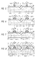
- Figs. 1 to 8 illustrate an embodiment in which the present invention is applied to a CMOS device.
- an N ⁇ -type well region 2 is formed by the drive-in diffusion of ion-implanted phosphorus or arsenic, while the P ⁇ -type well region 3 is formed by the drive-in diffusion of ion-implanted boron.
- the impurity concentration of each of the N ⁇ -type well region 2 and the P ⁇ -type well region 3 is approximately 2 x 10¹⁶ atoms/cm3. Further, as shown in Fig.
- the field insulator film 4 is formed by the thermal oxidation of the substrate 1 so as to define regions where elements are to be formed.
- a gate insulator film 6 which is about 15nm thick is formed on each of the element forming regions by the thermal oxidation of the substrate 1.
- an N-type impurity for example, As 7 or Sb 7 for adjusting the threshold voltages of both a P-channel MISFET and an N-channel MISFET is introduced into the surface of the substrate 1 by ion implantation at 60 keV and 5 x 10¹¹ atoms/cm2.
- diffusion coefficients are Sb « As « B.
- a polycrystalline silicon film 8A to constitute gate electrodes 8 is formed on the gate insulator films 6 overlying the substrate 1 to a thickness of about 200 nm by, for example, plasma CVD.
- a P-type impurity for example, boron is introduced into the polycrystalline silicon film 8A at 10 keV and 2 x 10¹⁵ atoms/cm2 so as to turn this film into the P+-type.
- a WSi2 film 8B to constitute the gate electrodes 8 is formed on the polycrystalline silicon film 8A to a thickness of about 200 nm by, for example, CVD.
- the WSi2 film 8B may well be a film of a refractory metal such as W, Mo, Ta, Ti or Pd or a film of any silicide of the refractory metal.
- a silicon oxide film 9 is further formed thereon at a thickness of about 80 nm by, for example, CVD.
- the silicon oxide film 9 serves to prevent As from entering the gate electrodes 8 at the ion implantation of the As which is performed later in order to form the source and drain regions of the N-channel MISFET Accordingly, this silicon oxide film is not especially required if the concentration of the boron in the P+-type polycrystalline silicon film 8A is high to the extent that this film 8A is not inverted into the N-type by the ion implantation at the step of forming the source and drain regions of the N-channel MISFET.
- the silicon oxide film 9, WSi2 film 8B and P+-type polycrystalline silicon film 8A are successively etched by etching which uses a mask made of a resist film not shown.
- Each of the gate electrodes 8 is made of a double-layer film which consists of the P+-type polycrystalline silicon film 8A and the WSi2 film 8B. After the etching, the mask made of the resist film is removed.
- a P-channel MISFET region (a region other than a region for forming the N-channel MISFET) is covered with a mask made of a resist film not shown, whereupon using the silicon oxide film 9 and the gate electrode 8 as a mask, P (phosphorus) is introduced into the N-channel MISFET forming region at, for example, 60 keV and 1 x 10¹³ atoms/cm2, thereby to form shallow ion-implanted layers of low impurity concentration 10A which constitute the source and drain regions of the N-channel MISFET.
- the mask made of the resist film is removed.
- a mask made of a resist film and covering the N-channel MISFET region is formed anew, and using the silicon oxide film 9 and the gate electrode 8 as a mask, boron is introduced into the P-channel MISFET forming region at, for example, 40 keV and 1 x 10¹³ atoms/cm2, thereby to form shallow ion-implanted layers of low impurity concentration 11A which constitute the source and drain regions of the P-channel MISFET After the ion implantation, the mask made of the resist film is removed.
- the resultant substrate is annealed at about 900°C to activate all of the impurity 7 for controlling the threshold voltages, the impurity of the N ⁇ -type regions 10A and the impurity of the P ⁇ -type regions 11A.
- the impurity 7 is hardly driven into the substrate 1 because the diffusion coefficient thereof is very small.
- a silicon oxide film having a thickness of about 400nm is formed on the whole surface of the substrate 1 by, for example, CVD, and it is etched back by reactive ion etching (RIE), thereby to form side walls 12 on both side surfaces of the gate electrodes 8.
- RIE reactive ion etching
- the P-channel MISFET region (on the N-type well 2) is covered with a mask made of a resist film not shown, and As is introduced into the N-channel MISFET forming region at 80 keV and approximately 5 x 10¹⁵ atoms/cm2 by ion implantation employing the gate electrode 8, silicon oxide film 9 and side walls 12 as a mask, thereby to form deep ion-implanted layers of high impurity concentration 10B which constitute the source and drain regions of the N-channel MISFET. After the ion implantation, the mask made of the resist film is removed.
- a mask made of a resist film and covering the N-channel MISFET region (the region other than the N-type well) is formed anew, and B (boron) is introduced into the P-channel MISFET region at 10 keV and approximately 2 x 10¹⁵ atoms/cm2 by ion implantation employing the gate electrode 8, silicon oxide film 9 and side walls 12 as a mask, thereby to form deep ion-implanted layers of high impurity concentration 11B which constitute the source and drain regions of the P-channel MISFET.
- the mask made of the resist film is removed.
- the N+-type regions 10B and the P ⁇ -type regions 11B are activated by annealing at about 950°C.
- the N-type impurity 7 for adjusting the threshold voltages spreads into the substrate 1 very little because the diffusion coefficient thereof is very small.
- an inter-layer insulator film 13 in which a phosphosilicate glass (PSG) film is stacked on a silicon oxide film deposited by, for example, plasma CVD; contact holes 14; and wiring 15 which comprises an aluminum film deposited by, for example, sputtering.
- PSG phosphosilicate glass
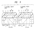
- a depletion layer spreading from each of the N ⁇ -type regions 10A or the P ⁇ -type regions 11A is illustrated in model fashion at letter D. It is assumed in Fig. 9 that the N ⁇ -type region 10A and the P ⁇ -type region 11A on the right sides are the drain regions, while the N ⁇ -type region 10A and the P ⁇ -type region 11A on the left sides are the source regions.
- the N-type impurity As or Sb is used as the impurity 7 for adjusting the threshold voltages.
- the depth of the junction formed between the P ⁇ -type well region 3 and the N ⁇ - or N-type region 7 by the impurity 7 becomes about 0.05 ⁇ m, which is very small as compared with the depth of a junction in the case of using the P-type impurity of boron as an impurity for adjusting threshold voltages.
- the junction part between the region 7 and the well region 3 does not further enlarge that part of the depletion layer of the drain region which is greatly spread. Accordingly, neither the punch-through between the source and the drain nor the change of the threshold voltage takes place.
- the N ⁇ -type well region 2 and the impurity 7 for adjusting the threshold voltage have the same conductivity type, so that a P-N junction is not defined in the channel region, and the spread of the depletion layer of the drain region is not promoted.
- the threshold voltage V th is expressed by: 0 ⁇ MS Difference between the work functions of the gate electrode and the substrate (silicon) 0 ⁇ F Fermi level of silicon Q B Quantity of charges in the substrate C OX Capacitance of the gate oxide film
- the impurity concentrations of the N ⁇ -type well region 2 and the P ⁇ -type well region 3 in this embodiment are both 2 x 10¹⁶ atoms/cm3, and the work function differences 0 ⁇ MS between them and the P+-type polycrystalline silicon film 8A are 0.92 eV and 0.18 eV, respectively.
- the values 2 0 ⁇ F of the N ⁇ -type well region 2 and the P ⁇ -type well region 3 are -0.74 eV and 0.74 eV, respectively.
- the value Q B /C OX of the N ⁇ -type well region 2 is -0.37 V, and that of the P ⁇ -type well region 3 is 0.37 V.
- an N-channel MISFET of the enhancement mode having a threshold voltage of about 0.6 V can be fabricated by forming the N ⁇ - or N-type region 7 in the channel region of the N-channel MISFET which has the gate electrode 8 including the P+-type polycrystalline silicon film as a part thereof. That is, the P+-type polycrystalline silicon film 8A is used as a part of the gate electrode 8 in order that the N-channel MISFET having the N ⁇ -type region 7 or N-type region 7 in the channel region may be rendered the enhancement mode, whereby an enhancement-mode N-channel MISFET having a threshold voltage of about 0.6 V can be fabricated.
- the threshold voltage is made too high merely by introducing the N-type impurity 7 into the channel region, and hence, the P+-type polycrystalline silicon film 8A is used as a part of the gate electrode 8, whereby an enhancement-mode P-channel MISFET having a threshold voltage of about -0.6 V can be fabricated.
- the N-channel MISFET and P-channel MISFET are used as, for example, elements which constitute the basic cell of a gate array.
- the gate electrode 8 of the N-channel MISFET and that of the P-channel MISFET are formed to be unitary, the interdiffusion of the impurities does not take place because both the members of the polycrystalline silicon film 8A constituting the gate electrodes are of the P+-type. That is, the threshold voltages do not fluctuate due to the interdiffusion of the impurities contained in the gate electrodes 8.
- a threshold voltage is controlled by the N-type impurity, for example, As or Sb of a channel region and the P+-type polycrystalline silicon film of a gate electrode, whereby in a P-channel MISFET, a P-N junction is not formed in the channel region, so that the spread of a depletion layer from a drain region is not promoted, and in an N-channel MISFET, even when a P-N junction is formed in the channel region, the depth thereof is as very small as about 0.05 ⁇ m from the surface of a substrate, so that the part of the depletion layer of a drain region having a great spread is not further enlarged. Accordingly, the fluctuations of the threshold voltages and punch-through become difficult to occur in both the P-channel MISFET and the N-channel MISFET, so that the short channels of the MISFETs can be attained.
- the N-type impurity for example, As or Sb of a channel region and the P+-type polycrystalline silicon film of a gate electrode
- the gate electrodes of the N-channel MISFET and the P-channel MISFET are both made of a poly-cide utilizing P+-type polycrystalline silicon, so that the problem of the inerdiffusion of impurities between the gate electrodes of the N-channel MISFET and the P-channel MISFET does not occur in the process of manufacture.
- an identical gate electrode can be shared by the P-channel and N-channel MISFETs, and a CMOS device suited to a high density of integration can be realized.
- the structure of the source or drain of a MISFET may be constructed only of a deep ion-implanted layer, or that of the drain may well be a DDD (Double Doped Drain) structure which is constructed of a diffused layer of low impurity concentration and a diffused layer of high impurity concentration.
- the material of a gate is not restricted to P-type polycrystalline silicon or a poly-cide utilizing P-type polycrystalline silicon, but it may be any material with which a plus work function difference is afforded relative to a semiconductor substrate.
Landscapes
- Engineering & Computer Science (AREA)
- Power Engineering (AREA)
- Microelectronics & Electronic Packaging (AREA)
- Physics & Mathematics (AREA)
- Condensed Matter Physics & Semiconductors (AREA)
- General Physics & Mathematics (AREA)
- Computer Hardware Design (AREA)
- Ceramic Engineering (AREA)
- Chemical & Material Sciences (AREA)
- Crystallography & Structural Chemistry (AREA)
- Manufacturing & Machinery (AREA)
- Metal-Oxide And Bipolar Metal-Oxide Semiconductor Integrated Circuits (AREA)
Abstract
Description
- The present invention relates to a semiconductor integrated circuit device and a method of manufacturing the same. More particularly, it relates to a technique which is effective when applied to the microfabrication of a MISFET.
- The threshold voltage of a MISFET of the enhancement mode has been controlled by introducing a P-type impurity, namely, boron into a channel region, in both a P-channel MISFET and an N-channel MISFET. The reason is that an N⁺-type polycrystalline silicon film being lower in resistance than a P⁺-type polycrystalline silicon film has been employed as the material of a gate electrode. When the gate electrode is made of the N⁺-type polycrystalline silicon film, the threshold voltage becomes low in the N-channel MISFET, and it becomes high in the P-channel MISFET. Therefore, the threshold voltage of each of the P-channel and N-channel MISFETs has been rendered about 0.6 V by introducing boron into the channel region thereof.
- In an N-type well region where the P-channel MISFET to which such a technique is applied is constructed, a P-N junction is defined in the deep part (about 0.2 µm deep) of the channel region. This is ascribable to the fact that, since the diffusion coefficient of boron is great, the boron introduced into the channel region diffuses deep into a substrate. Here, a depletion layer from the drain region of the MISFET spreads in the deep part of the substrate more than in the surface thereof. When the P-N junction is formed in the deep part of the channel region as stated above, the depletion layer from the drain region has its spread promoted by this P-N junction and comes to exert influence on the edge of a depletion layer from the source region of the MISFET. Therefore, when the reduction of a channel length has been attained, the threshold voltage becomes different from a design value, or punch-through arises across the source region and the drain region. It is accordingly impossible to reduce the channel length of the MISFET, that is, to achieve a short channel.
- By the way, a technique for shortening a channel is described in "IEDM Technical Digest," 1986, pp. 252 - 255.
- The aforementioned technique for shortening the channels of a CMOS device consists in that the gate electrode of a P-channel MISFET is formed of poly-cide utilizing a P⁺-type polycrystalline silicon film, while the gate electrode of an N-channel MISFET is formed of poly-cide utilizing an N⁺-type polycrystalline silicon film. The respective gate electrodes of the N-channel and P-channel MISFETs are formed by patterning the poly-cides which have been formed in such a way that N-type and P-type impurities are introduced into the selected parts of polycrystalline silicon deposited on the whole surface of a substrate and are activated, whereupon TaSi₂ is deposited on the polycrystalline silicon. However, when the gate electrodes of both the N- and P-channel MISFETs are formed to be unitary in this manner, interdiffusion of the impurities develops between the P⁺-type polycrystalline silicon film and the N⁺-type polycrystalline silicon film due to annealing carried out in the process of manufacture, and the threshold voltages of the MISFETs to be formed become unstable due to fluctuations in the difference between the work functions of the gate electrodes and the substrate. For the purpose of preventing this drawback, a device needs to be manufactured by annealing at or below about 800°C. Annealing at such a low temperature, however, incurs the problem that the formation of diffused layers and insulator films becomes difficult. Moreover, in a device wherein the gate electrodes of a P-channel MISFET and an N-channel MISFET are separated, wiring for connecting these gate electrodes is required, which is problematic when there is a high density of integration.
- It is desirable to achieve the microfabrication of a MISFET.
- It is also desirable to provide a semiconductor device and a method of manufacturing the same, which can produce a CMOS device of good "threshold voltage - channel length" characteristics without spoiling the high operating speed and the high integration density of the CMOS device.
- The above and other desiderata that may be achievable by embodiments of the present invention will become more apparent from the description of this specification and the accompanying drawings.
- A typical aspect of performance of the present invention is briefly summarized as follows:
- Each of the threshold voltages of an N-channel MISFET and a P-channel MISFET is controlled by the N-type impurity of a channel region, for example, As or Sb and the P⁺-type polycrystalline silicon film of a gate electrode.
- According to the expedient described above, owing to the use of the N-type impurity As or Sb as an impurity for adjusting the threshold voltage, in the P-channel MISFET, a P-N junction is not formed in the channel region thereof, and hence, the spread of a depletion layer from the drain region of the MISFET is not promoted. In the N-channel MISFET, even when a P-N junction is formed in the channel region thereof, the depth of the junction is as very small as approximately 0.05 µm from the surface of a substrate, so that the part of the depletion layer from the drain region of the MISFET having a great spread is not further enlarged. In both the P-channel MISFET and the N-channel MISFET, accordingly, the fluctuations of the threshold voltages and punch-through become difficult to occur, and hence, the short channels of the MISFETs can be realized. Moreover, since the gate electrodes are made of polycrystalline silicon of the same conductivity type in both the P-channel and N-channel MISFETs, the impurity interdiffusion between both the gates can be prevented during the process of manufacture, and a CMOS device of high reliability can be produced.
-
- Figs. 1 to 8 are processing sectional views showing an embodiment of a method of manufacturing a CMOS device to which the present invention is applied; and
- Fig. 9 is an enlarged sectional view of the channel region portions of a P-channel MISFET and an N-channel MISFET.
- Figs. 1 to 8 illustrate an embodiment in which the present invention is applied to a CMOS device.
- First, as shown in Fig. 1, an N⁻-
type well region 2, a P⁻-type well region 3, afield insulator film 4 and a P-type channel stopper 5 are respectively formed in or on asemiconductor substrate 1 made of P⁻⁻-type single-crystal silicon by well-known processes. The N⁻-type well region 2 is formed by the drive-in diffusion of ion-implanted phosphorus or arsenic, while the P⁻-type well region 3 is formed by the drive-in diffusion of ion-implanted boron. The impurity concentration of each of the N⁻-type well region 2 and the P⁻-type well region 3 is approximately 2 x 10¹⁶ atoms/cm³. Further, as shown in Fig. 1, thefield insulator film 4 is formed by the thermal oxidation of thesubstrate 1 so as to define regions where elements are to be formed. Agate insulator film 6 which is about 15nm thick is formed on each of the element forming regions by the thermal oxidation of thesubstrate 1. - Subsequently, as shown in Fig. 2, an N-type impurity, for example, As 7 or
Sb 7 for adjusting the threshold voltages of both a P-channel MISFET and an N-channel MISFET is introduced into the surface of thesubstrate 1 by ion implantation at 60 keV and 5 x 10¹¹ atoms/cm². Here, diffusion coefficients are Sb « As « B. By employing Sb or As for the adjustments of the threshold voltages, accordingly, a P-N junction to be defined between the impurity and the P⁻-type well region 3 can be formed shallow to the extent of 0.05 µm. - Next, as shown in Fig. 3, a
polycrystalline silicon film 8A to constitutegate electrodes 8 is formed on thegate insulator films 6 overlying thesubstrate 1 to a thickness of about 200 nm by, for example, plasma CVD. Also, a P-type impurity, for example, boron is introduced into thepolycrystalline silicon film 8A at 10 keV and 2 x 10¹⁵ atoms/cm² so as to turn this film into the P⁺-type. - Next, as shown in Fig. 4, a
WSi₂ film 8B to constitute thegate electrodes 8 is formed on thepolycrystalline silicon film 8A to a thickness of about 200 nm by, for example, CVD. Incidentally, the WSi₂film 8B may well be a film of a refractory metal such as W, Mo, Ta, Ti or Pd or a film of any silicide of the refractory metal. After theWSi₂ film 8B has been formed, asilicon oxide film 9 is further formed thereon at a thickness of about 80 nm by, for example, CVD. Thesilicon oxide film 9 serves to prevent As from entering thegate electrodes 8 at the ion implantation of the As which is performed later in order to form the source and drain regions of the N-channel MISFET Accordingly, this silicon oxide film is not especially required if the concentration of the boron in the P⁺-typepolycrystalline silicon film 8A is high to the extent that thisfilm 8A is not inverted into the N-type by the ion implantation at the step of forming the source and drain regions of the N-channel MISFET. - Next, as shown in Fig. 5, the
silicon oxide film 9,WSi₂ film 8B and P⁺-typepolycrystalline silicon film 8A are successively etched by etching which uses a mask made of a resist film not shown. Each of thegate electrodes 8 is made of a double-layer film which consists of the P⁺-typepolycrystalline silicon film 8A and theWSi₂ film 8B. After the etching, the mask made of the resist film is removed. Subsequently, a P-channel MISFET region (a region other than a region for forming the N-channel MISFET) is covered with a mask made of a resist film not shown, whereupon using thesilicon oxide film 9 and thegate electrode 8 as a mask, P (phosphorus) is introduced into the N-channel MISFET forming region at, for example, 60 keV and 1 x 10¹³ atoms/cm², thereby to form shallow ion-implanted layers oflow impurity concentration 10A which constitute the source and drain regions of the N-channel MISFET. After the ion implantation, the mask made of the resist film is removed. Subsequently, a mask made of a resist film and covering the N-channel MISFET region is formed anew, and using thesilicon oxide film 9 and thegate electrode 8 as a mask, boron is introduced into the P-channel MISFET forming region at, for example, 40 keV and 1 x 10¹³ atoms/cm², thereby to form shallow ion-implanted layers oflow impurity concentration 11A which constitute the source and drain regions of the P-channel MISFET After the ion implantation, the mask made of the resist film is removed. Thereafter, the resultant substrate is annealed at about 900°C to activate all of theimpurity 7 for controlling the threshold voltages, the impurity of the N⁻-type regions 10A and the impurity of the P⁻-type regions 11A. On this occasion, theimpurity 7 is hardly driven into thesubstrate 1 because the diffusion coefficient thereof is very small. - Next, as shown in Fig. 6, a silicon oxide film having a thickness of about 400nm is formed on the whole surface of the
substrate 1 by, for example, CVD, and it is etched back by reactive ion etching (RIE), thereby to formside walls 12 on both side surfaces of thegate electrodes 8. The length of eachside wall 12 in the channel length direction of the MOSFET is about 300nm. - Next, as shown in Fig. 7, the P-channel MISFET region (on the N-type well 2) is covered with a mask made of a resist film not shown, and As is introduced into the N-channel MISFET forming region at 80 keV and approximately 5 x 10¹⁵ atoms/cm² by ion implantation employing the
gate electrode 8,silicon oxide film 9 andside walls 12 as a mask, thereby to form deep ion-implanted layers ofhigh impurity concentration 10B which constitute the source and drain regions of the N-channel MISFET. After the ion implantation, the mask made of the resist film is removed. Subsequently, a mask made of a resist film and covering the N-channel MISFET region (the region other than the N-type well) is formed anew, and B (boron) is introduced into the P-channel MISFET region at 10 keV and approximately 2 x 10¹⁵ atoms/cm² by ion implantation employing thegate electrode 8,silicon oxide film 9 andside walls 12 as a mask, thereby to form deep ion-implanted layers ofhigh impurity concentration 11B which constitute the source and drain regions of the P-channel MISFET. After the ion implantation, the mask made of the resist film is removed. Thereafter, the N⁺-type regions 10B and the P⁻-type regions 11B are activated by annealing at about 950°C. On this occasion, the N-type impurity 7 for adjusting the threshold voltages spreads into thesubstrate 1 very little because the diffusion coefficient thereof is very small. - At the next step, as shown in Fig. 8, there are formed an
inter-layer insulator film 13 in which a phosphosilicate glass (PSG) film is stacked on a silicon oxide film deposited by, for example, plasma CVD;contact holes 14; andwiring 15 which comprises an aluminum film deposited by, for example, sputtering. - Here, the respective channel regions of the P-channel MISFET and the N-channel MISFET are shown on enlarged scale in Fig. 9.
- Referring to Fig. 9, a depletion layer spreading from each of the N⁻-
type regions 10A or the P⁻-type regions 11A is illustrated in model fashion at letter D. It is assumed in Fig. 9 that the N⁻-type region 10A and the P⁻-type region 11A on the right sides are the drain regions, while the N⁻-type region 10A and the P⁻-type region 11A on the left sides are the source regions. - In the present invention, the N-type impurity As or Sb is used as the
impurity 7 for adjusting the threshold voltages. In the N-channel MISFET region, therefore, the depth of the junction formed between the P⁻-type well region 3 and the N⁻- or N-type region 7 by theimpurity 7 becomes about 0.05 µm, which is very small as compared with the depth of a junction in the case of using the P-type impurity of boron as an impurity for adjusting threshold voltages. For this reason, the junction part between theregion 7 and thewell region 3 does not further enlarge that part of the depletion layer of the drain region which is greatly spread. Accordingly, neither the punch-through between the source and the drain nor the change of the threshold voltage takes place. On the other hand, in the P-channel MISFET, the N⁻-type well region 2 and theimpurity 7 for adjusting the threshold voltage have the same conductivity type, so that a P-N junction is not defined in the channel region, and the spread of the depletion layer of the drain region is not promoted. - Here, as is well known, the threshold voltage Vth is expressed by:

0̸F Fermi level of silicon
QB Quantity of charges in the substrate
COX Capacitance of the gate oxide film - The impurity concentrations of the N⁻-
type well region 2 and the P⁻-type well region 3 in this embodiment are both 2 x 10¹⁶ atoms/cm³, and the work function differences 0̸MS between them and the P⁺-typepolycrystalline silicon film 8A are 0.92 eV and 0.18 eV, respectively. In addition, thevalues 2 0̸F of the N⁻-type well region 2 and the P⁻-type well region 3 are -0.74 eV and 0.74 eV, respectively. Besides, the value QB/COX of the N⁻-type well region 2 is -0.37 V, and that of the P⁻-type well region 3 is 0.37 V. When calculated by substituting these values into the above expression, the threshold voltage of the P-channel MISFET without the introduction of the impurity into the channel region becomes -0.19 V, and the similar threshold voltage of the N-channel MISFET becomes 1.29 V. - Accordingly, an N-channel MISFET of the enhancement mode having a threshold voltage of about 0.6 V can be fabricated by forming the N⁻- or N-
type region 7 in the channel region of the N-channel MISFET which has thegate electrode 8 including the P⁺-type polycrystalline silicon film as a part thereof. That is, the P⁺-typepolycrystalline silicon film 8A is used as a part of thegate electrode 8 in order that the N-channel MISFET having the N⁻-type region 7 or N-type region 7 in the channel region may be rendered the enhancement mode, whereby an enhancement-mode N-channel MISFET having a threshold voltage of about 0.6 V can be fabricated. On the other hand, in the P-channel MISFET, the threshold voltage is made too high merely by introducing the N-type impurity 7 into the channel region, and hence, the P⁺-typepolycrystalline silicon film 8A is used as a part of thegate electrode 8, whereby an enhancement-mode P-channel MISFET having a threshold voltage of about -0.6 V can be fabricated. - By the way, although the plan pattern thereof is not depicted, the N-channel MISFET and P-channel MISFET are used as, for example, elements which constitute the basic cell of a gate array. In this case, even when the
gate electrode 8 of the N-channel MISFET and that of the P-channel MISFET are formed to be unitary, the interdiffusion of the impurities does not take place because both the members of thepolycrystalline silicon film 8A constituting the gate electrodes are of the P⁺-type. That is, the threshold voltages do not fluctuate due to the interdiffusion of the impurities contained in thegate electrodes 8. - Effects which are produced by typical aspects of performance of the present invention will be briefly explained below:
- A threshold voltage is controlled by the N-type impurity, for example, As or Sb of a channel region and the P⁺-type polycrystalline silicon film of a gate electrode, whereby in a P-channel MISFET, a P-N junction is not formed in the channel region, so that the spread of a depletion layer from a drain region is not promoted, and in an N-channel MISFET, even when a P-N junction is formed in the channel region, the depth thereof is as very small as about 0.05 µm from the surface of a substrate, so that the part of the depletion layer of a drain region having a great spread is not further enlarged. Accordingly, the fluctuations of the threshold voltages and punch-through become difficult to occur in both the P-channel MISFET and the N-channel MISFET, so that the short channels of the MISFETs can be attained.
- Moreover, the gate electrodes of the N-channel MISFET and the P-channel MISFET are both made of a poly-cide utilizing P⁺-type polycrystalline silicon, so that the problem of the inerdiffusion of impurities between the gate electrodes of the N-channel MISFET and the P-channel MISFET does not occur in the process of manufacture. In consequence, an identical gate electrode can be shared by the P-channel and N-channel MISFETs, and a CMOS device suited to a high density of integration can be realized.
- Although, in the above, the present invention has been concretely described in conjunction with the embodiments, it is needless to say that the present invention is not restricted to the foregoing embodiments, but that it can be variously altered within a scope not departing from the purport thereof.
- By way of example, the structure of the source or drain of a MISFET may be constructed only of a deep ion-implanted layer, or that of the drain may well be a DDD (Double Doped Drain) structure which is constructed of a diffused layer of low impurity concentration and a diffused layer of high impurity concentration. In addition, the material of a gate is not restricted to P-type polycrystalline silicon or a poly-cide utilizing P-type polycrystalline silicon, but it may be any material with which a plus work function difference is afforded relative to a semiconductor substrate.
Claims (18)
a semiconductor substrate (1) of first conductivity type; and
MISFETs formed on said semiconductor substrate, each of the MISFETs being provided with:
a gate electrode (8) which includes a P⁺-type polycrystalline silicon film;
first semiconductor regions of second conductivity type opposite to the first conductivity type, which are formed in said semiconductor substrate (1) and which are source and drain regions, respectively, and a second semiconductor region (7) which is formed by introducing an N-type impurity into a part of said semiconductor substrate under said gate electrode and which is shallower than said first semiconductor region;
wherein a threshold voltage of said each MISFET is controlled by said polycrystalline silicon film and the N-type impurity which forms said second semiconductor region (7).
a semiconductor substrate (1) of first conductivity type;
a well region (2) of the first conductivity type and a well region (3) of second conductivity type, which are formed in said semiconductor substrate (1); and
first and second groups of at least one MISFET which are formed on said semiconductor substrate, and each MISFET of which is provided with a gate electrode (8) which includes a P⁺-type polycrystalline silicon film, semiconductor regions (10,11) which are source and drain regions formed in said semiconductor substrate (1), respectively, and a first semiconductor region (7) which is formed by introducing an N-type impurity into a part of said semiconductor substrate (1) under said gate electrode (8), the N-type impurity of said first semiconductor region controlling the threshold voltages of each of the MISFETs conjointly with said P⁺-type polycrystalline silicon film, the first and second groups of said MISFETs being respectively formed in said well region (2) of the first conductivity type and said well region (3) of the second conductivity type;
wherein one of the first and second groups consists of P-channel MISFETs, said semiconductor regions (11) of each of which are second semiconductor regions of P-type, and wherein the other of the first and second groups consists of N-channel MISFETs, said semiconductor regions (10) of each of which are third semiconductor regions of N-type.
Applications Claiming Priority (2)
| Application Number | Priority Date | Filing Date | Title |
|---|---|---|---|
| JP62229523A JPS6473676A (en) | 1987-09-16 | 1987-09-16 | Semiconductor integrated circuit device |
| JP229523/87 | 1987-09-16 |
Publications (2)
| Publication Number | Publication Date |
|---|---|
| EP0308152A2 true EP0308152A2 (en) | 1989-03-22 |
| EP0308152A3 EP0308152A3 (en) | 1991-01-09 |
Family
ID=16893503
Family Applications (1)
| Application Number | Title | Priority Date | Filing Date |
|---|---|---|---|
| EP19880308388 Withdrawn EP0308152A3 (en) | 1987-09-16 | 1988-09-12 | Mis integrated circuit device and method of manufacturing the same |
Country Status (3)
| Country | Link |
|---|---|
| EP (1) | EP0308152A3 (en) |
| JP (1) | JPS6473676A (en) |
| KR (1) | KR890005891A (en) |
Cited By (5)
| Publication number | Priority date | Publication date | Assignee | Title |
|---|---|---|---|---|
| EP0414226A2 (en) * | 1989-08-24 | 1991-02-27 | Nec Corporation | MOS field-effect transistor with sidewall spacers |
| US5170232A (en) * | 1989-08-24 | 1992-12-08 | Nec Corporation | MOS field-effect transistor with sidewall spacers |
| EP0543268A2 (en) * | 1991-11-19 | 1993-05-26 | Texas Instruments Incorporated | Transistor device with a gate structure and method of forming the same |
| US5407839A (en) * | 1991-11-01 | 1995-04-18 | Seiko Epson Corporation | MOS manufacturing process having reduced gate insulator defects |
| WO1997036321A1 (en) * | 1996-03-27 | 1997-10-02 | Advanced Micro Devices, Inc. | Process to separate the doping of polygate and source drain regions |
Families Citing this family (8)
| Publication number | Priority date | Publication date | Assignee | Title |
|---|---|---|---|---|
| JP2776891B2 (en) * | 1989-06-19 | 1998-07-16 | 株式会社日立製作所 | Semiconductor integrated circuit device |
| WO1997008752A1 (en) * | 1995-08-25 | 1997-03-06 | Hitachi, Ltd. | Mis semiconductor device |
| JP4898013B2 (en) * | 2001-04-04 | 2012-03-14 | セイコーインスツル株式会社 | Semiconductor device |
| JP2002313940A (en) * | 2001-04-10 | 2002-10-25 | Seiko Instruments Inc | Method of manufacturing semiconductor device |
| JP4865152B2 (en) * | 2001-06-19 | 2012-02-01 | セイコーインスツル株式会社 | Manufacturing method of semiconductor device |
| JP2003007846A (en) * | 2001-06-21 | 2003-01-10 | Seiko Instruments Inc | Semiconductor device |
| JP4898024B2 (en) * | 2001-06-21 | 2012-03-14 | セイコーインスツル株式会社 | Manufacturing method of semiconductor device |
| JP2009044002A (en) * | 2007-08-09 | 2009-02-26 | Ricoh Co Ltd | Semiconductor device, and temperature-sensing device using same |
Citations (2)
| Publication number | Priority date | Publication date | Assignee | Title |
|---|---|---|---|---|
| US4242691A (en) * | 1978-09-18 | 1980-12-30 | Mitsubishi Denki Kabushiki Kaisha | MOS Semiconductor device |
| EP0187260A2 (en) * | 1984-12-03 | 1986-07-16 | Hitachi, Ltd. | Process for fabricating a semiconductor integrated circuit device having MISFETs |
-
1987
- 1987-09-16 JP JP62229523A patent/JPS6473676A/en active Pending
-
1988
- 1988-08-31 KR KR1019880011148A patent/KR890005891A/en not_active Application Discontinuation
- 1988-09-12 EP EP19880308388 patent/EP0308152A3/en not_active Withdrawn
Patent Citations (2)
| Publication number | Priority date | Publication date | Assignee | Title |
|---|---|---|---|---|
| US4242691A (en) * | 1978-09-18 | 1980-12-30 | Mitsubishi Denki Kabushiki Kaisha | MOS Semiconductor device |
| EP0187260A2 (en) * | 1984-12-03 | 1986-07-16 | Hitachi, Ltd. | Process for fabricating a semiconductor integrated circuit device having MISFETs |
Non-Patent Citations (2)
| Title |
|---|
| 1986 SYMPOSIUM ON VLSI TECHNOLOGY, DIGEST OF TECHNICAL PAPERS, San Diego 1986, pages 19-20, IEEE, New York, US; T. NOGUCHI et al.: "High speed CMOS structure with optimized gate work function" * |
| INTERNATIONAL ELECTRON DEVICES MEETING, Washington, D.C., 8th - 10th December 1980, pages 791-794, IEEE, New York, US; E. SUN et al.: "The junction MOS (JMOS) transistor- a high speed transistor for VLSI" * |
Cited By (8)
| Publication number | Priority date | Publication date | Assignee | Title |
|---|---|---|---|---|
| EP0414226A2 (en) * | 1989-08-24 | 1991-02-27 | Nec Corporation | MOS field-effect transistor with sidewall spacers |
| EP0414226A3 (en) * | 1989-08-24 | 1991-04-03 | Nec Corporation | Mos field-effect transistor with sidewall spacers |
| US5170232A (en) * | 1989-08-24 | 1992-12-08 | Nec Corporation | MOS field-effect transistor with sidewall spacers |
| US5407839A (en) * | 1991-11-01 | 1995-04-18 | Seiko Epson Corporation | MOS manufacturing process having reduced gate insulator defects |
| EP0543268A2 (en) * | 1991-11-19 | 1993-05-26 | Texas Instruments Incorporated | Transistor device with a gate structure and method of forming the same |
| EP0543268A3 (en) * | 1991-11-19 | 1993-08-11 | Texas Instruments Incorporated | Transistor device with a gate structure and method of forming the same |
| WO1997036321A1 (en) * | 1996-03-27 | 1997-10-02 | Advanced Micro Devices, Inc. | Process to separate the doping of polygate and source drain regions |
| US6319804B1 (en) | 1996-03-27 | 2001-11-20 | Advanced Micro Devices, Inc. | Process to separate the doping of polygate and source drain regions in dual gate field effect transistors |
Also Published As
| Publication number | Publication date |
|---|---|
| KR890005891A (en) | 1989-05-17 |
| JPS6473676A (en) | 1989-03-17 |
| EP0308152A3 (en) | 1991-01-09 |
Similar Documents
| Publication | Publication Date | Title |
|---|---|---|
| US5254866A (en) | LDD CMOS with wider oxide sidewall on PMOS than NMOS | |
| KR0134756B1 (en) | Semiconductor device and manufacture method thereof | |
| US5278441A (en) | Method for fabricating a semiconductor transistor and structure thereof | |
| US4703552A (en) | Fabricating a CMOS transistor having low threshold voltages using self-aligned silicide polysilicon gates and silicide interconnect regions | |
| US5397715A (en) | MOS transistor having increased gate-drain capacitance | |
| US4562638A (en) | Method for the simultaneous manufacture of fast short channel and voltage-stable MOS transistors in VLSI circuits | |
| US5294822A (en) | Polycide local interconnect method and structure | |
| US4849364A (en) | Semiconductor devices | |
| EP0166167B1 (en) | A process for manufacturing a semiconductor device comprising p-channel and n-channel misfets | |
| US4698659A (en) | Stacked complementary metal oxide semiconductor inverter | |
| KR100420870B1 (en) | Method of producing an eeprom semiconductor structure | |
| EP0308152A2 (en) | MIS integrated circuit device and method of manufacturing the same | |
| US4488348A (en) | Method for making a self-aligned vertically stacked gate MOS device | |
| US4784966A (en) | Self-aligned NPN bipolar transistor built in a double polysilicon CMOS technology | |
| US6027964A (en) | Method of making an IGFET with a selectively doped gate in combination with a protected resistor | |
| US5005066A (en) | Self-aligned NPN bipolar transistor built in a double polysilicon CMOS technology | |
| KR0172116B1 (en) | Method of manufacturing a semiconductor device | |
| EP0337481A2 (en) | Semiconductor device | |
| GB2088129A (en) | An integrated circuit mosfet and a method of making the same | |
| US5691564A (en) | Semiconductor device with high speed operation and high integration | |
| JP2845899B2 (en) | Method for manufacturing semiconductor integrated circuit device | |
| EP0568206B1 (en) | Bipolar transistor and method of manufacture | |
| JP2886186B2 (en) | Semiconductor device | |
| JP2845934B2 (en) | Method for manufacturing semiconductor integrated circuit device | |
| JPH0855914A (en) | Cmos semiconductor device and manufacture thereof |
Legal Events
| Date | Code | Title | Description |
|---|---|---|---|
| PUAI | Public reference made under article 153(3) epc to a published international application that has entered the european phase |
Free format text: ORIGINAL CODE: 0009012 |
|
| AK | Designated contracting states |
Kind code of ref document: A2 Designated state(s): DE FR GB IT |
|
| PUAL | Search report despatched |
Free format text: ORIGINAL CODE: 0009013 |
|
| AK | Designated contracting states |
Kind code of ref document: A3 Designated state(s): DE FR GB IT |
|
| 17P | Request for examination filed |
Effective date: 19910708 |
|
| 17Q | First examination report despatched |
Effective date: 19930405 |
|
| STAA | Information on the status of an ep patent application or granted ep patent |
Free format text: STATUS: THE APPLICATION IS DEEMED TO BE WITHDRAWN |
|
| 18D | Application deemed to be withdrawn |
Effective date: 19930817 |