EP0307988B1 - Oszillatorschaltung mit Amplitudenregler - Google Patents
Oszillatorschaltung mit Amplitudenregler Download PDFInfo
- Publication number
- EP0307988B1 EP0307988B1 EP88201860A EP88201860A EP0307988B1 EP 0307988 B1 EP0307988 B1 EP 0307988B1 EP 88201860 A EP88201860 A EP 88201860A EP 88201860 A EP88201860 A EP 88201860A EP 0307988 B1 EP0307988 B1 EP 0307988B1
- Authority
- EP
- European Patent Office
- Prior art keywords
- transistor
- current
- junction point
- oscillator circuit
- control electrode
- Prior art date
- Legal status (The legal status is an assumption and is not a legal conclusion. Google has not performed a legal analysis and makes no representation as to the accuracy of the status listed.)
- Expired - Lifetime
Links
Images
Classifications
-
- H—ELECTRICITY
- H03—ELECTRONIC CIRCUITRY
- H03B—GENERATION OF OSCILLATIONS, DIRECTLY OR BY FREQUENCY-CHANGING, BY CIRCUITS EMPLOYING ACTIVE ELEMENTS WHICH OPERATE IN A NON-SWITCHING MANNER; GENERATION OF NOISE BY SUCH CIRCUITS
- H03B5/00—Generation of oscillations using amplifier with regenerative feedback from output to input
- H03B5/08—Generation of oscillations using amplifier with regenerative feedback from output to input with frequency-determining element comprising lumped inductance and capacitance
- H03B5/12—Generation of oscillations using amplifier with regenerative feedback from output to input with frequency-determining element comprising lumped inductance and capacitance active element in amplifier being semiconductor device
-
- H—ELECTRICITY
- H03—ELECTRONIC CIRCUITRY
- H03L—AUTOMATIC CONTROL, STARTING, SYNCHRONISATION OR STABILISATION OF GENERATORS OF ELECTRONIC OSCILLATIONS OR PULSES
- H03L5/00—Automatic control of voltage, current, or power
Definitions
- the invention relates to an oscillator circuit comprising
- An oscillator circuit of this kind is known from European Patent Application EP-A-0 050 583, Figure 2.
- a voltage control system comprising two current sources supplying currents of different polarity on the control terminal constitutes a sensitive control system because of the high impedance of a current source. Small current variations are then converted into large voltage variations.
- one of the current sources comprises a current path of a first PMOS transistor which is connected to the high supply voltage and the other current source comprises a path of an NMOS transistor which is connected to a low supply voltage via a resistor.
- the control electrode of the first PMOS transistor is connected, via a current path of a further MOS transistor, to a junction point between two series-connected current paths of a second and a third PMOS transistor which both are connected as a diode.
- the series connection of the diodes is connected on the one side to the high supply voltage and on the other side to the low supply voltage, via a reference current source.
- the control electrode of the further MOS transistor is connected to the junction point between the diode series connection and the reference current source.
- the oscillator voltage is coupled, via a capacitance, to the control electrode of the first PMOS transistor.
- the oscillation voltage coupled through via the capacitance generates voltage fluctuations on the control electrode of the first PMOS transistor.
- a current flows through the further transistor in one direction, which current is substantially independent of the magnitude of the voltage on the latter control electrode, or a current flow in the opposite direction, which current is exponentially dependent on the control voltage of the further transistor.
- the exponential dependency being due to the fact that the further transistor operates below its threshold, implies an exponential temperature dependency.
- the resistor whereby the NMOS transistor is connected to the low supply voltage is an undesirable component which requires a substantial substrate surface area. If a substantially temperature-independent behaviour is required, the resistor can be constructed as a metal film resistor for which additional connection pins are required on the IC.
- the invention inter alia aims to provide an oscillator circuit of the kind set forth which has a simpler set-up and which comprises fewer components.
- an oscillator circuit in accordance with the invention is characterized in that the amplitude detector comprises a series connection of current paths of a first and second transistor of a first and second conductivity type, respectively, a control electrode of the first transistor being connected to the feedback circuit so that the amplitude is detected during at the most one half of an oscillation period, a control electrode of the second transistor being connected to a first junction point between the first and second transistor, the first junction point being coupled for controlling a current supplied by the at least one of the first and second current source.
- the amplitude is controlled on the basis of fluctuations of one given polarity, and fewer components suffice because the magnitude of the amplitude need no longer be compared with a mean (floating) value but rather with, for example one of the supply voltages or a threshold voltage of a transistor.
- An embodiment of the oscillator circuit according to the invention is characterized, in that the first and second current source comprise respectively a third transistor and a fourth transistor of the first and second conductivity type, respectively, with their current paths connected in series, a control electrode of the fourth transistor being connected to the first junction point, the third transistor conducting a reference current, a third junction point, between the current paths of the third and fourth transistor being connected to the control terminal.
- the amplitude detector connected to the feedback circuit controls the voltage on the control electrode of the second transistor via the current mirror formed by the second transistor and the fourth transistor.
- a further embodiment of an oscillator circuit in accordance with the invention is characterized in that the amplifier comprises a series connection of the current paths of a fifth and sixth transistor of the first and second conductivity type, respectively, and in which the feedback circuit is connected between a control electrode of the fifth transistor on the one side and a second junction point between the current paths of the fifth and sixth transistors on the other side, a control electrode of the sixth transistor constituting said control terminal.
- the amplitude controller is thus coupled to the power supply terminal of the amplifier.
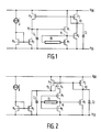
- Fig. 1 shows a first embodiment of an oscillator circuit in accordance with the invention.
- the amplifier comprises the series connection of transistors N1 and P1 between power supply terminals V DD and V SS . Between the junction point K1 of these transistors and the control terminal of the transistor N1 there is connected the feedback network, for example in the form of a semiconductor delay line DL. The length and the process variables, such as the sheet resistance and the sheet capacitance, of this delay line DL determine the oscillator frequency.
- the amplitude detector formed by the series connection of transistors N2 and P2, has an input connected to the junction point K1. The output of the amplitude detector, being the junction point K2, is connected to the control electrode of a transistor P3 which is connected in series with a transistor N3.
- the control terminal of the latter transistor receives a reference voltage associated with a conducted current equal or proportional to I ref .
- the transistor P3 and the transistor N3 thus form the current sources.
- Their junction point K3 is connected to the control terminal of the transistor P1.
- the buffer capacitances C2 and C3 are connected to the junction points K2 and K3, respectively. Because of their integrating effect, these capacitances slightly reduce the control sensitivity.
- the operation is as follows. At the start, the transistors N2, P2 and P3 are blocked. The reference current then forces the transistor N3 to reduce the control voltage at the junction point K3, so that the transistor P1 is conductive on to a high degree. Oscillation starts as soon as the current conducted by P1 is sufficiently large to satisfy the oscillation condition. The transistor N2 then transforms the positive oscillation fluctuation into a current which is integrated on the capacitance C2. The voltage across C2 then decreases, with the result that the transistor P3 becomes conductive. The potential at the junction point K3 then increases, so that the current passage through the transistor P1 is adjusted to a lower value.
- Fig. 2 shows a second embodiment of the oscillator circuit in accordance with the invention.
- the oscillator consists of, for example the amplifier N1/P1 which is fed back via the delay line DL.
- the amplitude detector N2/P2 connected to the output thereof controls the current source P3 which is connected in series with the reference current source N3.
- the amplifier N1/P1 is fed via the transistor P4, a control electrode of which is connected to the junction point K3 between the current sources P3 and N3.
- the transistor P4 is also provided in order to achieve quick starting.
Landscapes
- Inductance-Capacitance Distribution Constants And Capacitance-Resistance Oscillators (AREA)
Claims (6)
- Oszillatorschaltung mit- einem Verstarker (N1), der mittels einer Regelspannung an einem Regelanschluß (K3) regelbar ist und eine zwischen einem Verstärkereingang und einem Verstärkerausgang (K1) angeordnete Rückkopplungsschaltung (DL) enthält,- einem Amplitudenregler (N2, P2, N3, P3), der einen Amplitudendetektor (N2, P2) zur Regelung der Schwingungsamplitude in Abhängigkeit von einer detektierten Amplitude sowie auch eine erste und zweite Stromquelle (N3, P3) zum Liefern von Strömen mit einander entgegengesetzter Polarität an dem Regelanschluß (K3) enthält, wobei von der ersten und der zweiten Stromquelle (N3, P3) mindestens eine durch den Amplitudendetektor (N2, P2) regelbar ist,
dadurch gekennzeichnet, daß der Amplitudendetektor eine Reihenschaltung aus Strompfaden eines ersten und eines zweiten Transistors (N2, P2) eines ersten bzw. eines zweiten Leitungstyp enthält, wobei eine Steuerelektrode des ersten Transistors (N2) mit der Rückkopplungsschaltung (DL) verbunden ist, so daß die Amplitude während höchstens einer Hälfte einer Schwingungsperiode detektiert wird, wobei eine Steuerelektrode des zweiten Transistors (P2) mit einem ersten Knotenpunkt (K2) zwischen dem ersten und dem zweiten Transistor verbunden ist, und wobei der erste Knotenpunkt (K2) zur Regelung eines von mindestens einer der ersten und der zweiten Stromquelle gelieferten Stroms gekoppelt ist. - Oszillatorschaltung nach Anspruch 1, dadurch gekennzeichnet, daß die Steuerelektrode des ersten Transistors (N2) mit dem Verstärkerausgang (K1) verbunden ist.
- Oszillatorschaltung nach Anspruch 1 oder 2, dadurch gekennzeichnet, daß die erste und die zweite Stromquelle einen dritten Transistor (N3) bzw. einen vierten Transistor (P3) des ersten bzw. zweiten Leitungstyps umfassen, deren Strompfade in Reihe geschaltet sind, wobei eine Steuerelektrode des vierten Transistors (P3) mit dem ersten Knotenpunkt (K2) verbunden ist, der dritte Transistor (N3) einen Bezugsstrom führt, und ein dritter, zwischen den Strompfaden des dritten (N3) und vierten (P3) Transistors liegender Knotenpunkt (K3) mit dem Regelanschluß verbunden ist.
- Oszillatorschaltung nach Anspruch 1, 2 oder 3, dadurch gekennzeichnet, daß der Verstärker eine Reihenschaltung der Strompfade eines fünften und eines sechsten Transistors (N1; P1, Figur 1 oder P4, Figur 2) des ersten bzw. des zweiten Leitungstyps enthält, und in der die Rückkopplungsschaltung (DL) zwischen eine Steuerelektrode des fünften Transistors (N1) einerseits und einen zweiten Knotenpunkt (K1) zwischen den Strompfaden des fünften und sechsten Transistors andererseits geschaltet ist, und eine Steuerelektrode des sechsten Transistors den genannten Regelanschluß (K3) bildet.
- Oszillatorschaltung nach Anspruch 4, dadurch gekennzeichnet, daß der Verstärker einen siebten Transistor (P1, Figur 2) enthält, dessen Strompfad zwischen den fünften und den sechsten Transistor in Reihe geschaltet ist und dessen Steuerelektrode mit der Rückkopplungsschaltung verbunden ist.
- Oszillatorschaltung nach einem der Ansprüche 1 bis 5, dadurch gekennzeichnet, daß mindestens eine der folgenden Pufferkapazitäten vorhanden ist:- eine erste Pufferkapazität (C2) zwischen dem ersten Knotenpunkt (K2) und einem von zwei Spannungsversorgungsanschlüssen (Vdd, Vss);- eine zweite Pufferkapazität zwischen dem dritten Knotenpunkt (K3) und einem von zwei Spannungsversorgungsanschlüssen (Vdd, Vss).
Applications Claiming Priority (2)
| Application Number | Priority Date | Filing Date | Title |
|---|---|---|---|
| NL8702122 | 1987-09-08 | ||
| NL8702122A NL8702122A (nl) | 1987-09-08 | 1987-09-08 | Oscillatorschakeling met amplituderegelaar. |
Publications (2)
| Publication Number | Publication Date |
|---|---|
| EP0307988A1 EP0307988A1 (de) | 1989-03-22 |
| EP0307988B1 true EP0307988B1 (de) | 1993-03-31 |
Family
ID=19850572
Family Applications (1)
| Application Number | Title | Priority Date | Filing Date |
|---|---|---|---|
| EP88201860A Expired - Lifetime EP0307988B1 (de) | 1987-09-08 | 1988-08-31 | Oszillatorschaltung mit Amplitudenregler |
Country Status (6)
| Country | Link |
|---|---|
| US (1) | US4901037A (de) |
| EP (1) | EP0307988B1 (de) |
| JP (1) | JP3004019B2 (de) |
| KR (1) | KR970004438B1 (de) |
| DE (1) | DE3879832T2 (de) |
| NL (1) | NL8702122A (de) |
Families Citing this family (15)
| Publication number | Priority date | Publication date | Assignee | Title |
|---|---|---|---|---|
| US5073900A (en) * | 1990-03-19 | 1991-12-17 | Mallinckrodt Albert J | Integrated cellular communications system |
| KR19990064076A (ko) * | 1996-08-07 | 1999-07-26 | 요트.게.아. 롤페즈 | 발진기 |
| RU2191474C1 (ru) * | 2001-03-23 | 2002-10-20 | Ипатьев Василий Михайлович | Способ передачи информации на подвижные объекты |
| RU2191475C1 (ru) * | 2001-03-23 | 2002-10-20 | Ипатьев Василий Михайлович | Способ передачи информации на подвижные объекты |
| RU2194364C1 (ru) * | 2001-03-23 | 2002-12-10 | Ипатьев Василий Михайлович | Способ передачи информации на подвижные объекты |
| RU2193816C1 (ru) * | 2001-03-23 | 2002-11-27 | Ипатьев Василий Михайлович | Способ передачи информации на подвижные объекты |
| RU2191476C1 (ru) * | 2001-03-23 | 2002-10-20 | Ипатьев Василий Михайлович | Способ передачи информации на подвижные объекты |
| RU2195775C2 (ru) * | 2001-03-23 | 2002-12-27 | Ипатьев Василий Михайлович | Способ передачи информации на подвижные объекты |
| RU2191473C1 (ru) * | 2001-03-23 | 2002-10-20 | Ипатьев Василий Михайлович | Способ передачи информации на подвижные объекты |
| RU2193817C1 (ru) * | 2001-03-23 | 2002-11-27 | Ипатьев Василий Михайлович | Способ передачи информации на подвижные объекты |
| RU2193818C1 (ru) * | 2001-03-23 | 2002-11-27 | Ипатьев Василий Михайлович | Способ передачи информации на подвижные объекты |
| RU2187895C1 (ru) * | 2001-03-23 | 2002-08-20 | Ипатьев Василий Михайлович | Способ передачи информации на подвижные объекты |
| RU2193819C1 (ru) * | 2001-03-23 | 2002-11-27 | Ипатьев Василий Михайлович | Способ передачи информации на подвижные объекты |
| RU2187894C1 (ru) * | 2001-03-23 | 2002-08-20 | Ипатьев Василий Михайлович | Способ передачи информации на подвижные объекты |
| US7295081B2 (en) * | 2005-08-29 | 2007-11-13 | Micron Technology, Inc. | Time delay oscillator for integrated circuits |
Family Cites Families (4)
| Publication number | Priority date | Publication date | Assignee | Title |
|---|---|---|---|---|
| CH642228B (fr) * | 1980-10-16 | Ebauches Electroniques Sa | Convertisseur d'une tension alternative en un courant continu et circuit oscillateur comprenant de convertisseur. | |
| DE3223338C2 (de) * | 1982-06-23 | 1987-02-19 | EUROSIL electronic GmbH, 8057 Eching | Integrierte Feldeffekttransistor-Oszillatorschaltung |
| NL8304085A (nl) * | 1983-11-29 | 1985-06-17 | Philips Nv | Oscillatorschakeling. |
| US4560958A (en) * | 1984-02-24 | 1985-12-24 | Tektronix, Inc. | State variable oscillator having improved rejection of leveler-induced distortion |
-
1987
- 1987-09-08 NL NL8702122A patent/NL8702122A/nl not_active Application Discontinuation
-
1988
- 1988-08-31 DE DE88201860T patent/DE3879832T2/de not_active Expired - Fee Related
- 1988-08-31 EP EP88201860A patent/EP0307988B1/de not_active Expired - Lifetime
- 1988-09-01 US US07/239,574 patent/US4901037A/en not_active Expired - Lifetime
- 1988-09-06 KR KR1019880011481A patent/KR970004438B1/ko not_active Expired - Fee Related
- 1988-09-06 JP JP63221492A patent/JP3004019B2/ja not_active Expired - Lifetime
Also Published As
| Publication number | Publication date |
|---|---|
| KR890005967A (ko) | 1989-05-18 |
| DE3879832D1 (de) | 1993-05-06 |
| KR970004438B1 (ko) | 1997-03-27 |
| JP3004019B2 (ja) | 2000-01-31 |
| JPS6472603A (en) | 1989-03-17 |
| EP0307988A1 (de) | 1989-03-22 |
| US4901037A (en) | 1990-02-13 |
| NL8702122A (nl) | 1989-04-03 |
| DE3879832T2 (de) | 1993-09-30 |
Similar Documents
| Publication | Publication Date | Title |
|---|---|---|
| EP0307988B1 (de) | Oszillatorschaltung mit Amplitudenregler | |
| EP0039946B1 (de) | Integrierte Halbleiter-Schaltungsvorrichtung | |
| US4346343A (en) | Power control means for eliminating circuit to circuit delay differences and providing a desired circuit delay | |
| US5072197A (en) | Ring oscillator circuit having improved frequency stability with respect to temperature, supply voltage, and semiconductor process variations | |
| EP0661616A2 (de) | Bandlückenspannungsreferenzgenerator | |
| US5285173A (en) | Signal-controlled ring oscillator with delay cells having constant gain with change in frequency | |
| US4893095A (en) | Frequency stabilized oscillator | |
| EP0116689B1 (de) | Geregelter Substratvorspannungsgenerator | |
| US4760353A (en) | Integrated gyrator oscillator | |
| US6476669B2 (en) | Reference voltage adjustment | |
| EP0039178B1 (de) | Integrierte Schaltung zum Erzeugen einer Referenzspannung | |
| EP0121793B1 (de) | CMOS-Kreis mit parameterangepasstem Spannungsregler | |
| GB2292858A (en) | Bias circuit for low voltage bipolar amplifier | |
| US4199693A (en) | Compensated MOS timing network | |
| KR100331400B1 (ko) | 반도체회로 | |
| EP0582072A1 (de) | Temperaturkompensierter Spannungsregler mit Beta-Kompensation | |
| US5136183A (en) | Integrated comparator circuit | |
| US20020158679A1 (en) | Voltage control circuit | |
| KR940027322A (ko) | 반도체 집적회로장치 | |
| US5900771A (en) | Capacitive multiplier for timing generation | |
| US7692477B1 (en) | Precise control component for a substrate potential regulation circuit | |
| US4996499A (en) | Amplitude stabilized oscillator amplifier | |
| US7049833B2 (en) | Method for optimizing the accuracy of an electronic circuit | |
| US4424457A (en) | Voltage level detecting circuit | |
| KR0167562B1 (ko) | 전류 임계 검출기 회로 |
Legal Events
| Date | Code | Title | Description |
|---|---|---|---|
| PUAI | Public reference made under article 153(3) epc to a published international application that has entered the european phase |
Free format text: ORIGINAL CODE: 0009012 |
|
| AK | Designated contracting states |
Kind code of ref document: A1 Designated state(s): CH DE FR GB IT LI |
|
| 17P | Request for examination filed |
Effective date: 19890919 |
|
| 17Q | First examination report despatched |
Effective date: 19910808 |
|
| GRAA | (expected) grant |
Free format text: ORIGINAL CODE: 0009210 |
|
| AK | Designated contracting states |
Kind code of ref document: B1 Designated state(s): CH DE FR GB IT LI |
|
| PG25 | Lapsed in a contracting state [announced via postgrant information from national office to epo] |
Ref country code: IT Free format text: LAPSE BECAUSE OF FAILURE TO SUBMIT A TRANSLATION OF THE DESCRIPTION OR TO PAY THE FEE WITHIN THE PRESCRIBED TIME-LIMIT;WARNING: LAPSES OF ITALIAN PATENTS WITH EFFECTIVE DATE BEFORE 2007 MAY HAVE OCCURRED AT ANY TIME BEFORE 2007. THE CORRECT EFFECTIVE DATE MAY BE DIFFERENT FROM THE ONE RECORDED. Effective date: 19930331 |
|
| REF | Corresponds to: |
Ref document number: 3879832 Country of ref document: DE Date of ref document: 19930506 |
|
| ET | Fr: translation filed | ||
| PLBE | No opposition filed within time limit |
Free format text: ORIGINAL CODE: 0009261 |
|
| STAA | Information on the status of an ep patent application or granted ep patent |
Free format text: STATUS: NO OPPOSITION FILED WITHIN TIME LIMIT |
|
| 26N | No opposition filed | ||
| REG | Reference to a national code |
Ref country code: FR Ref legal event code: CD |
|
| REG | Reference to a national code |
Ref country code: FR Ref legal event code: CD |
|
| PGFP | Annual fee paid to national office [announced via postgrant information from national office to epo] |
Ref country code: FR Payment date: 20010824 Year of fee payment: 14 |
|
| PGFP | Annual fee paid to national office [announced via postgrant information from national office to epo] |
Ref country code: GB Payment date: 20010831 Year of fee payment: 14 |
|
| PGFP | Annual fee paid to national office [announced via postgrant information from national office to epo] |
Ref country code: DE Payment date: 20011015 Year of fee payment: 14 |
|
| PGFP | Annual fee paid to national office [announced via postgrant information from national office to epo] |
Ref country code: CH Payment date: 20011114 Year of fee payment: 14 |
|
| REG | Reference to a national code |
Ref country code: GB Ref legal event code: IF02 |
|
| PG25 | Lapsed in a contracting state [announced via postgrant information from national office to epo] |
Ref country code: LI Free format text: LAPSE BECAUSE OF THE APPLICANT RENOUNCES Effective date: 20020831 Ref country code: GB Free format text: LAPSE BECAUSE OF NON-PAYMENT OF DUE FEES Effective date: 20020831 Ref country code: CH Free format text: LAPSE BECAUSE OF THE APPLICANT RENOUNCES Effective date: 20020831 |
|
| REG | Reference to a national code |
Ref country code: CH Ref legal event code: PL |
|
| PG25 | Lapsed in a contracting state [announced via postgrant information from national office to epo] |
Ref country code: DE Free format text: LAPSE BECAUSE OF NON-PAYMENT OF DUE FEES Effective date: 20030301 |
|
| GBPC | Gb: european patent ceased through non-payment of renewal fee |
Effective date: 20020831 |
|
| PG25 | Lapsed in a contracting state [announced via postgrant information from national office to epo] |
Ref country code: FR Free format text: LAPSE BECAUSE OF NON-PAYMENT OF DUE FEES Effective date: 20030430 |
|
| REG | Reference to a national code |
Ref country code: FR Ref legal event code: ST |