EP0304035A2 - Bi-mos circuit capable of high speed operation with low power consumption - Google Patents
Bi-mos circuit capable of high speed operation with low power consumption Download PDFInfo
- Publication number
- EP0304035A2 EP0304035A2 EP88113356A EP88113356A EP0304035A2 EP 0304035 A2 EP0304035 A2 EP 0304035A2 EP 88113356 A EP88113356 A EP 88113356A EP 88113356 A EP88113356 A EP 88113356A EP 0304035 A2 EP0304035 A2 EP 0304035A2
- Authority
- EP
- European Patent Office
- Prior art keywords
- channel mos
- mos transistor
- source
- drain
- transistor
- Prior art date
- Legal status (The legal status is an assumption and is not a legal conclusion. Google has not performed a legal analysis and makes no representation as to the accuracy of the status listed.)
- Granted
Links
Images


Classifications
-
- H—ELECTRICITY
- H03—ELECTRONIC CIRCUITRY
- H03K—PULSE TECHNIQUE
- H03K19/00—Logic circuits, i.e. having at least two inputs acting on one output; Inverting circuits
- H03K19/0008—Arrangements for reducing power consumption
- H03K19/0013—Arrangements for reducing power consumption in field effect transistor circuits
-
- H—ELECTRICITY
- H03—ELECTRONIC CIRCUITRY
- H03K—PULSE TECHNIQUE
- H03K19/00—Logic circuits, i.e. having at least two inputs acting on one output; Inverting circuits
- H03K19/02—Logic circuits, i.e. having at least two inputs acting on one output; Inverting circuits using specified components
- H03K19/08—Logic circuits, i.e. having at least two inputs acting on one output; Inverting circuits using specified components using semiconductor devices
- H03K19/094—Logic circuits, i.e. having at least two inputs acting on one output; Inverting circuits using specified components using semiconductor devices using field-effect transistors
- H03K19/0944—Logic circuits, i.e. having at least two inputs acting on one output; Inverting circuits using specified components using semiconductor devices using field-effect transistors using MOSFET or insulated gate field-effect transistors, i.e. IGFET
- H03K19/09448—Logic circuits, i.e. having at least two inputs acting on one output; Inverting circuits using specified components using semiconductor devices using field-effect transistors using MOSFET or insulated gate field-effect transistors, i.e. IGFET in combination with bipolar transistors [BIMOS]
Definitions
- the present invention relates to a Bi-MOS circuit and, more particularly, to a Bi-MOS circuit suitable for large-scale integrated circuits (hereinafter, referred to LSI's) such as gate arrays, memories and logic IC's.
- LSI's large-scale integrated circuits
- MOSFET metal-oxide-semiconductor field-effect transistors
- the composed elements must be miniaturized. If the miniaturized MOSFETs have a channel length shorter than 0.8 ⁇ m, the hot carrier injection and the lowered withstand voltage between source and drain become new problems. Those problem may be overcome by lowering power voltage.
- the lower power voltage decreases power dissipation to improve the integration density with the same total power consumption.
- the low power voltage however, deteriorates high speed operation and driving ability.
- the signal processing part was formed of a combination of a large number of fundamental circuits, that is, for example, basic cells in a gate-array device.
- the fundamental circuit cells were formed of Bi-MOS circuits for high speed operation.
- the voltage converter must be designed by using large size transistors and requires an extremely large area to lower the integration density.
- the voltage converter requires a coupling capacitor to avoid undesired oscillation.
- the capacitor occupies a large area to further decrease the integrated density.
- the driving ability of the bipolar circuit was not improved by the lowered power voltage.
- the Bi-MOS circuit in accordance with the present invention includes a field effect transistor having a gate connected to an input terminal, one of a source and a drain connected to a first fixed potential and the other end of the source and the drain, a bipolar transistor having a collector connected to a second fixed potential, an emitter connected to an output terminal and a base, a load element having a first terminal connected to both the other of the source and the drain of the field effect transistor and the base of the bipolar transistor and a second terminal connected to a third fixed potential having a potential value between the first and second fixed potential, and a switching element having a control electrode connected to both the input terminal and the gate of the field effect transistor, a third terminal connected to the first fixed potential and a fourth terminal connected to both the emitter of the bipolar transistor and the output terminal, the switching element connecting the third terminal to the fourth terminal when a first input signal which turns the field effect transistor on is inputted to the input terminal and disconnecting the third terminal from the fourth terminal when a second input signal which turns the field effect transistor off
- the field effect transistor is favorably an N-channel MOS transistor and the bipolar transistor is favorably an NPN transistor.
- the first fixed potential is a reference potential
- the third fixed potential is fixed higher than the first fixed potential
- the second fixed potential is fixed higher than the third fixed potential.
- both the N-channel MOS transistor and the switching element are turned off and the bipolar transistor is turned on.
- the voltage level of the output terminal is determined by the third fixed potential, the third fixed potential being lower than the second fixed potential. Therefore, the amplitude from on state to off state at the output terminal becomes small and the power consumption at the transient time becomes small.
- the collector of the bipolar transistor is connected to the second fixed potential which is higher than the third fixed potential, the collector-emitter saturation voltage V CE sat. is high. Therefore, the cut-off frequency f T is high and the collector current I C is large, resulting in a high speed operation and a large driving ability.
- both the N-channel MOS transistor and the switching element is turned on and the bipolar transistor is turned off, resulting in the low level at the output terminal.
- the charges in the base of the bipolar transistor are discharged rapidly by the N-channel MOS transistor, resulting in a high speed operation.
- the load element is favorably a P-channel MOS transistor to form a complementary MOS circuit with the N-channel MOS transistor.
- the power consumption is extremely small because of the C-MOS circuit configuration.
- the load element may be a resistor or a load MOS transistor of which the gate is connected to the one of the source and drain of the field effect transistor.
- the switching element is favorably constituted of an NPN bipolar transistor having a collector connected to the output terminal, an emitter connected to the first fixed potential and a base, an N-channel MOS transistor having one of a source and a drain connected to both the output terminal and the collector of this another NPN bipolar transistor, the other of the source and the drain connected to the base of this another NPN bipolar transistor and a gate electrode connected to the input terminal and a resistor connected between the first fixed potential and the connecting point between the other of the source and the drain of the N-channel MOS transistor and the base of this NPN bipolar transistor.
- the resistor may be replaced with an N-channel MOS transistor.
- the switching element is also favorably an N-channel MOS transistor having one of a source and a drain connected to the output terminal, the other of the source and the drain connected to the first fixed potential and a gate electrode connected to the input terminal.
- the bipolar transistor may be a PNP transistor, the field effect transistor being a P-channel MOS transistor, the third fixed potential being lower than the first fixed potential and the second fixed potential being lower than the third fixed potential.
- the low power consumption and the high speed operation can be obtained also in this case.
- an NPN bipolar transistor 17 and an NPN bipolar transistor 18 are connected in series between a high power source Vcc and the ground.
- a collector of the bipolar transistor 17 is connected to the high power source Vcc, an emitter being connected to collector of the transistor 18 and an output terminal 12.
- An emitter of the transistor 18 is connected to the ground.
- a P-channel MOS transistor 13 and an N-channel MOS transistor 14 are connected in series between a low power source V'cc which is lower than the high power source Vcc and the ground, each gate of these MOS transistor 13 and 14 being connected in common to an input terminal 11.
- a source of the P-channel MOS transistor 13 is connected to the lower power source V'cc, a drain being connected to a base of the NPN transistor 17 and a drain of the N-channel MOS transistor 14.
- a source of the N-channel MOS transistor 14 is connected to the ground.
- a drain of an N-channel MOS transistor 15 is connected to the output terminal 12, a gate being connected to the input terminal 11 and a source being connected not only to the ground through a resistor 16 but also to a base of the NPN transistor 18.
- the N-channel MOS transistors 14 and 15 and the NPN transistor 18 are on, the P-channel MOS transistor 13 and the NPN transistor 17 being off to make the output terminal 12 be at a low level.
- the N-channel MOS transistors 14 and 15 and the NPN transistor 18 are off, the P-channel MOS transistor 13 and the NPN transistor 17 being on to make the output terminal 12 be at a high level. Therefore, the NPN transistors 17 and 18 are not simultaneously in the "on" states not to consume power in the steady state.
- the N-channel MOS transistor 15 turns off and the charges stored in the base of the NPN transistor 18 are discharged quickly through the resistor 16. Therefore, the NPN transistor 18 turns off quickly to make all the current from the NPN transistor 17 flow into the load (not shown) connected to the output terminal 12.
- the P-channel MOS transistor 13 turns on to make the N-channel MOS transistor 14 turn off, causing the NPN transistor 17 to turn on quickly. As a result, a high level signal is produced at the output terminal 12.
- the source of the P-channel MOS transistor 13 is connected to the low power source V'cc (which is lower than the high power source Vcc) and thus the high level voltage at the output terminal 12 becomes V'cc - V BE (where V BE is the built-in voltage between the base and emitter of the NPN transistor 17), resulting in the small change from "on" state to "off” state at the output terminal 12.
- V BE is the built-in voltage between the base and emitter of the NPN transistor 17
- the P-channel transistor 13 turns off, the N-channel MOS transistor 14 turning on to quickly discharge charges stored in the base of the NPN transistor 17 through the N-channel MOS transistor 14, resulting in an "off" state of the NPN transistor 17.
- the N-channel MOS transistor 15 turns on and a part of the current flowing through the N-channel MOS transistor 15 to the ground is bypassed through the base of the NPN transistor 18 to turn on the NPN transistor 18 quickly. Accordingly, the output terminal 12 is changed from a high level to a low level.
- the charges stored in the base of the NPN transistor 17 and the NPN transistor 18 during their "on” states are discharged quickly by the N-channel transistor 14 and the resistor 16, respectively.
- the NPN transistor 18 is quickly turned on by the N-channel transistor 15 and the resistor 16. Consequently, the current flowing through both the NPN transistor 17 and the NPN transistor 18 at the transient time is suppressed and the power consumption at the transient time is remarkably reduced.
- the high power source Vcc is favorably supplied from outside the chip, the voltage of the high power source Vcc being ordinarily 5 V.
- the low power source V'cc is favorably supplied by converting the voltage supplied from the high power source Vcc with use of an internal voltage converter or a voltage regulator to a voltage of 3.3 V, ordinarily. In a case of 3.3 V of the low power supply V'cc, since the base-emitter built-in voltage V BE is about 0.7 V, the high level at the output terminal 12 is about 2.6 V.
- the voltage of low power supply V'cc may be 4.0 V to raise the high level at the output terminal 12 to 3.3 V.
- a P-channel MOS transistor 23 and an N-channel MOS transistor 24 are connected in series between the power source V'cc and the ground.
- a source of the P-channel MOS transistor 23 is connected to the power source V'cc, a drain of the P-channel transistor 23 being connected to both a drain of the N-channel transistor 24 and the gates of the MOS transistors 13, 14 and 15.
- a source of the N-channel MOS transistor 24 is connected to the ground.
- a register 21 and an NPN bipolar transistor 22 are connected in series between the high power source Vcc (which is higher than the low power source V'cc) and the ground.
- a collector of the NPN transistor 22 is connected not only to the high power source Vcc through the resistor 21 but also to the gates of the MOS transistors 23 and 24.
- a base of the NPN transistor 22 is connected to the input terminal 11, the emitter being connected to the ground.
- the circuit composed of the MOS transistors 13, 14 and 15, the resistor 16 and the NPN transistors 17 and 18 are the same as the first embodiment shown in Fig. 1.
- the NPN transistor 22 turns on to make the potential of its collector at the low level. Accordingly, the P-channel MOS transistor 23 turns on, the N-channel MOS transistor 24 turning off to raise the gate potential of the MOS transistors 13, 14 and 15 at a high level of V'cc which is equal to the low power source.
- the NPN transistor 22 turns off to make the potential of its collector at the high level. Accordingly, the P-channel MOS transistor 23 turns off, the N-channel MOS transistor turning on, resulting in making the gate potential of the MOS transistors 13, 14 and 15 at the low level.
- the gates of the MOS transistors 13, 14 and 15 are at the low level of ground at the input terminal 11 of high level, the gates of the MOS transistors 13, 14 and 15 being at the high level of V'cc in response to the input terminal 11 of low level.
- the change in amplitude from the low level to the high level at the gates of these MOS transistors 13, 14 and 15 is as small as from the ground to the V'cc (which is lower than Vcc), resulting in the low power consumption at the transient time.
- the circuit operation at the right-hand side of the MOS transistors 13, 14 and 15 is similar to those in Fig. 1.
- a NAND circuit having two input terminals 11a and 11b is constructed by using the inverter shown in Fig. 1.
- the NPN bipolar transistor 17 and the NPN bipolar transistor 18 are connected in series between the power source Vcc and the ground, the collector of the NPN bipolar transistor 17 being connected to Vcc, the emitter of the NPN transistor 17 being connected to both the output terminal 12 and the collector of the NPN transistor 18 and the emitter of the NPN transistor 18 being connected to the ground.
- a P-channel MOS transistors 13a and 13b are connected in parallel, both sources of these transistors 13a and 13b being connected to the low power source V'cc which supplies a voltage lower than the high power source Vcc, both drains of these transistors 13a and 13b being connected to the base of the NPN transistor 17, a gate of the P-channel MOS transistor 13a being connected to an input terminal 11a and a gate of the P-channel MOS transistor 13b being connected to an input terminal 11b.
- N-channel MOS transistors 14a and 14b are connected in series, a drain of the N-channel MOS transistor 14a being connected to the drains of the P-channel MOS transistors 13a and 13b and the base of the NPN transistor 17, a source of the N-channel MOS transistor 14a being connected a drain of the N-channel MOS transistor 14b, a source of the N-channel MOS transistor 14b being connected to the ground, a gate of the N-channel MOS transistor 14a being connected to the gate of the P-channel MOS transistor 13a and the input terminal 11a and a gate of the N-channel MOS transistor 14b being connected to the gate of the P-channel MOS transistor 13b and the input terminal 11b.
- An N-channel MOS transistor 15a and an N-channel MOS transistor 15b is connected in series, a drain of the N-channel MOS transistor 15a being connected to the output terminal 12, the emitter of the NPN transistor 17 and the collector of the NPN transistor 18, a source of the N-channel MOS transistor 15a being connected to a drain of the N-channel MOS transistor 15b, a source of the N-channel MOS transistor 15b being connected to the ground by the resistor 16 and also connected to the base of the NPN transistor 18, a gate of the N-channel MOS transistor 15a being connected to the gate of the P-channel MOS transistor 13a, the gate of the N-channel MOS transistor 14a and the input terminal 11a and a gate of the N-channel MOS transistor 15b being connected to the gate of the P-channel MOS transistor 13b, the gate of the N-channel MOS transistor 14b and the input terminal 11b.
- the bipolar transistors 17 and 18 changes quickly to avoide simultaneous "on" states, resulting in a low power consumption.
- the sources of the P-channel transistors 13a and 13b are connected to the low power source V'cc which is lower than the high power source Vcc, the high level at the output terminal 12 is V'cc - V BE , resulting in the small change in output level from the low level to the high level. Accordingly, the power consumption at the transient time becomes small. Furthermore, the collector of the NPN transistor 17 is connected to the high power source Vcc which is higher than the low power source V'cc and the NPN transistor 17 operates at a high speed with large driving ability as same as the inverter shown in Fig. 1.
- the resistor 16 in the inverter shown in Fig. 1 is replaced by an N-channel MOS transistor 25.
- the circuit operation is similar to the inverter shown in Fig. 1.
- the switching speed of this inverter is smaller than the inverter with the resistor 16 such as shown in Fig. 1, but the pattern layout is more simple than the inverter having the resistor 16 such as shown in Fig. 1.
- the N-channel MOS transistor 13 in the inverter shown in Fig. 1 is replaced by a resistor 33.
- the N-channel MOS transistor 13 in the inverter shown in Fig. 1 is replaced by a load MOS transistor 43.
- the base current always flows into the base of the NPN transistor 17 through the resistor 33 or the load MOS transistor 43 and the current flows from the power source V'cc to the ground.
- the frequency of the signal applied to the input terminal 11 is high, for example, when higher than 100 MHz, the increase in the power consumption based on this constant base current is negligible.
- the high level at the output terminal 12 is V'cc - V BE . Since V'cc is ordinarily chosen as 3.3 V and the built-in voltage V BE is about 0.7 V, the high level at the output terminal 12 is 2.6 V. Additionally, the base-emitter saturation voltage V BE of the NPN transistor 18 is about 0.7 V and the low level at the output terminal 12 is determined by the base-emitter built-in voltage V BE of 0.7 V due to the "on" of the N-channel MOS transistor 15. Therefore, the change in output level from the low level to the high level at the output terminal 12 becomes as small as 1.9 V and then a noise margin becomes small.
- the switching element constructed with the N-channel transistor 15, resistor 16 and the NPN bipolar transistor 18 is replaced in a 6th embodiment shown in Fig. 7 by an N-channel MOS transistors 51.
- a P-channel MOS transistor 13 and an N-channel MOS transistor 14 are connected in series to form a CMOS inverter, a source of the P-channel MOS transistor 13 being connected to a low power source V'cc which supplies a voltage lower than the high power source Vcc, a gate of the P-channel MOS transistor 13 being connected to the input terminal 11, a drain of the P-channel MOS transistor 13 being connected to a drain of the N-channel MOS transistor 14, a gate of the N-channel MOS transistor 14 being connected to the gate of the P-channel MOS transistor 13 and the input terminal 11 and a source of the N-channel MOS transistor 14 being connected to the ground.
- the NPN bipolar transistor 17 and an N-channel MOS transistor 51 are connected in series between the high power source Vcc and the ground, the collector of the NPN transistor 17 being connected to the high power source Vcc, the base of the NPN transistor 17 being connected to both the drains of the MOS transistors 13 and 14, an emitter of the NPN transistor 17 being connected to the output terminal 12 and a drain of the N-channel MOS transistor 51, a source of the N-channel MOS transistor being connected to the ground and a gate of the N-channel MOS transistor 51 being connected to the input terminal 11 and the gates of the MOS transistors 13 and 14.
- the P-channel MOS transistor 13 When the input terminal 11 is changed from the high level to the low level, the P-channel MOS transistor 13 turns on, the N-channel MOS transistors 14 and 51 turning off. Accordingly, all the current flowing through the P-channel MOS transistor 13 flows into the base of the NPN transistor 17 to turn the transistor 17 on quickly, resulting in a high level at the output terminal 12.
- the source of the P-channel MOS transistor 13 is connected to the low power source V'cc (which is lower than the high power source Vcc), the high level at the output terminal 12 is V'cc - V BE , resulting in the small change in output level at the output terminal 12 from the low level to the high level. Therefore, the power consumption at the transient time is small.
- the N-channel MOS transistor 51 in place of the bipolar transistor 18 in Fig. 1, the low level at the output terminal 12 is lowered to the ground. Accordingly, a large noise margin can be obtained although the high level at the output terminal 12 is lowered to V'cc - V BE .
- the collector of the NPN transistor 17 is connected to the high power source Vcc which is higher than the low power source V'cc, resulting in a high speed operation and a large driving ability.
- a NAND circuit having two input terminals 11a and 11b is constructed by utilizing the inverter shown in Fig. 7.
- the NPN bipolar transistor 17 and the N-channel MOS transistors 51a and 51b are connected in series between the power source Vcc and the ground, a collector of the NPN transistor 17 being connected to the high power source Vcc, an emitter of the NPN transistor 17 being connected to the output terminal 12 and a drain of the N-channel MOS transistor 51a, a gate of the N-channel MOS transistor 51a being connected to the input terminal 11a, a source of the N-channel MOS transistor 51a being connected to a drain of the N-channel MOS transistor 51b, a gate of the N-channel MOS transistor 51b being connected to the input terminal 11b and a source of the N-channel MOS transistor 51b being connected to the ground.
- a P-channel MOS transistors 13a and 13b are connected in parallel with each other, both sources of these transistors 13a and 13b being connected to the low power source V'cc which is lower than the high power source Vcc, both drains of these transistors 13a and 13b being connected to the base of the NPN transistor 17, a gate of the P-channel MOS transistor 13a being connected to the input terminal 11a and a gate of the P-channel transistor 13b being connected to the input terminal 11b.
- N-channel MOS transistors 14a and 14b are connected in series, a drain of the N-channel MOS transistor 14a being connected to the drains of the P-channel transistors 13a and 13b and the gate of the NPN-transistor 17, a source of the N-channel MOS transistor 14a being connected to a drain of the N-channel MOS transistor 14b, a gate of the N-channel MOS transistor 14a being connected to the input terminal 11a, a gate of the N-channel MOS transistor 14b being connected to the input terminal 11b and a source of the N-channel MOS transistor 14b being connected to the ground.
- both the P-channel MOS transistors 13a and 13b turn off, both the N-channel MOS transistors 14a and 14b turning on and both the N-channel MOS transistors 51a and 51b turning on. Therefore, the charges stored in the base of the NPN transistor 17 are discharged through the N-channel MOS transistors 14a and 14b, resulting in a low level at the output terminal 12.
- the sources of the P-channel MOS transistors 13a and 13b are connected to the low power source V'cc, the high level at the output terminal 12 is as small as V'cc - V BE , resulting in a low power consumption.
- the N-channel MOS transistors 51a and 51b in place of the bipolar transistor such as used in Fig. 1, the low level at the output terminal 12 is lowered to the ground. Therefore, a large noise margin can be maintained.
- the collector of the NPN transistor 17 is connected to the high power source Vcc, the NAND circuit can be operated at high speed with large driving ability.
- a NOR circuit having two input terminals 11a and 11b is constructed by utilizing the inverter shown in Fig. 7.
- a pair of the N-channel transistors 51c and 51d which are connected in a parallel with each other and the NPN bipolar transistor 17 are connected in series between the high power source Vcc and the ground, a collector of the NPN transistor 17 being connected to the high power source Vcc, an emitter of the NPN transistor 17 being connected to the output terminal 12 and both drains of the N-channel MOS transistors 51c and 51d, both sources of the N-channel MOS transistors 51c and 51d being connected to the ground, a gate of the N-channel MOS transistor 51c being connected to the input terminal 11a and a gate of the N-channel MOS transistor 51d being connected to the input terminal 11b.
- P-channel MOS transistors 13c and 13d are connected in series, a source of the P-channel MOS transistor 13c being connected to the low power source V'cc which is lower than the high power source Vcc, a drain of the P-channel MOS transistor 13c being connected to a source of the P-channel MOS transistor 13d, a drain of the P-channel MOS transistor 13d being connected to the base of the NPN transistor 17, a gate of the P-channel MOS transistor 13c being connected to the input terminal 11a and a gate of the P-channel MOS transistor 13d being connected to the input terminal 11b.
- N-channel MOS transistors 14c and 14d are connected in parallel with each other, both drains of these MOS transistors 14c and 14d being connected to the drain of the P-channel MOS transistor 13d and the base of the NPN transistor 17, both sources of the N-channel MOS transistors 14c and 14d being connected to the ground, a gare of the N-channel MOS transistor 14c being connected to the input terminal 11a and a gate of the N-channel MOS transistor 14d being connected to the input terminal 11b.
- At least one of the input terminals 11a and 11b is changed to the high level, at least one of the P-channel MOS transistors 13c and 13d turns off, at least one of the N-channel MOS transistors 14c and 14d turns on and at least one of the N-channel MOS transistors 51c and 51d turns on. Accordingly, the base of the NPN transistor 17 is discharged quickly by the N-channel MOS transistors 14c and 14d, resulting in the low level at the output terminal 12.
- both the P-channel MOS transistors 13c and 13d turn on, both the N-channel MOS transistors 14c and 14d turning off and both the N-channel MOS transistors 51c and 51d turn off. Accordingly, the base of the NPN transistor 17 is charged quickly by the P-channel MOS transistors 13c and 13d, resulting in the high level at the output terminal 12.
- the sources of the P-channel MOS transistor 13c being connected to the low power source V'cc, the high level at the output terminal 12 is as small as V'cc - V BE , resulting in the low power consumption during a transient period followed after an input change.
- the N-channel MOS transistors 51c and 51d in place of the bipolar transistor, the low level at the output terminal 12 is lowered to the ground. Therefore, a large noise margin can be similarly maintained.
- the collector of the NPN transistor 17 is connected to the high power source Vcc, the NOR circuit can be operated at high speed with large driving ability.
- a logic IC is constructed with an external power supply terminal 101, a signal input terminal 102, a signal output terminal 101, a voltage converter 103 which converts the external power voltage of, for example, 5 V to an internal power voltage of, for example, 3.3 V, a Bi-CMOS circuit 104 having internal gate circuits 120 and 120′, an output buffer 130 and a data-bus driver 140, Bi-CMOS circuits 150 and 150′, a CMOS circuit 160 having P-channel MOS transistors 161 and 161′ and N-channel MOS transistors 162 and 162′ and the power line being connected only to the external power supply terminal 101, a level shift circuit 170 and a CMOS circuit 180 having a P-channel MOS transistors 181, 181′ and 181 ⁇ and N-channel MOS transistors 182, 182′ and 182 ⁇ and the power line being connected only to the output of the voltage converter 103.
- the internal gates 120 has two input terminals 121a (121a′) and 121b (121b′), two P-channel MOS transistors 123a (123a′) and 123b (123b′), four N-channel MOS transistors 124a (124a′), 124b (124b′), 125a (125a′) and 125b (125b′), two NPN bipolar transistors 127 (127′) and 128 (128′), a resistor 126 (126′) and an output terminal 122 (122′).
- the sources of the P-channel MOS transistors 123a and 123b are connected to the output of the voltage converter 103.
- the collector of the NPN bipolar transistor 127 is connected to the external power supply terminal 101.
- This internal gate is the same NAND circuit as the one shown in Fig. 3.
- the output buffer 130 is the inverter as shown in Fig. 1, the buffer 130 having a P-channel MOS transistor 133, N-channel MOS transistors 134 and 135, a resistor 136 and NPN transistors 137 and 138, the source of the P-channel MOS transistor 133 being connected to the output of the voltage converter 103 and the collector of the NPN transistor 137 being connected to the external power supply terminal 101.
- the data-bus driver 140 is the inverter as shown in Fig.
- the driver 140 having a P-channel MOS transistor 143, N-channel MOS transistors 144 and 145, a resistor 146 and NPN transistors 147 and 148, the source of the P-channel MOS transistor 143 being connected to the output of the voltage converter 103 and the collector of the NPN transistor 147 being connected to the external power supply terminal 101.
- the signals processed in the Bi-CMOS circuit 104 is outputted to the output terminal 110 by the output buffer 130.
- the CMOS circuit 150 (150′) also has the inverter as shown in Fig. 1.
- This inverter has a P-channel MOS transistors 153 (153′), N-channel MOS transistors 154 (154′) and 155 (155′), a register 156 (156′) and the NPN transistors 157 (157′) and 158 (158′), the source of the P-channel MOS transistor 153 (153′) being connected to the output of the voltage converter 103 and the collector of the NPN transistor 157 (157′) being connected to the external power supply terminal 101.
- the voltage converter 103 which converts the external power voltage of 5 V to the internal power voltage of 3.3 V
- the logic amplitude in the Bi-CMOS circuits 104, 150 and 150′ is small, resulting in the low power consumption.
- the power for the NPN bipolar transistors 127 (127′), 137, 147 and 157 (157′) is supplied from the external power supply through the external power supply terminal 101, the cut-off frequency f T is held at high and the collector current I C is large, resulting in a high speed operation and the large driving ability.
- the voltage converter 103 which supplies the power to the CMOS circuit without supplying the power to the bipolar circuit does not show the instability.
- a DRAM circuit is constructed with address input terminals 201, 201′, address buffers 202, 202′, decoders 203, 203′, word line drivers 204, 204′, a sense amplifier SA, bit lines BL, BL , word lines WL1, WL2, memory cells with N-channel MOS transistors 206, 206′ and memory cell capacitors Cs1, Cs2, and a precharge circuit 205.
- the word line driver circuit 204 is constructed with the inverter shown in Fig. 4.
- the collector of the NPN transistor 17 is connected to an external power source Vcc of 5 V, the source of the P-channel MOS transistor 13 being connected to an internal power source V'cc of 3.3 V supplied by an internal power converter.
- the emitter of the NPN transistor 18 is connected to an power source of -V BE to make the low logic level at the output terminal 12 0 V.
- a SRAM circuit is constructed with an address input terminal 301, an address buffer 302, decoders 303, 303′, word line drivers 304, 304′, memory cells 311, 311′, word lines WL1, WL2 and bit lines BL and BL .
- the word line driver 304 is constructed with the inverter shown in Fig. 4.
- the collector of the NPN transistor 17 is connected to an external power source 308 of 5 V, the source of the P-channel MOS transistor 13 being connected to an internal power source 307 of 3.3 V supplied by an internal power converter (not shown). Since the emitter of the NPN transistor 18 is connected to the ground, the low level at the output terminal 12 of this inverter is higher than the ground potential by the base-emitter built-in potential V BE of about 0.7 V.
- the memory cell 311 is constructed with N-channel MOS transistors 321, 322, 323 and 324 and the resistors 325 and 326, these resistors 325 and 326 being connected to an internal power source 307 of 3.3 V.
- the word line driver 304 is constructed with the inverter shown in Fig. 7.
- the collector of the NPN transistor 17 is connected to the external power source 308 of 5 V
- the source of the P-channel MOS transistor 13 is connected to the internal power source 307 of 3.3 V supplied by an internal power converter (not shown). Since the N-channel MOS transistor 51 is used in place of the NPN transistor 18 shown in Fig. 14, the low level at the output terminal 12 is lowered to the ground level, resulting in a large logic amplitude from the low level to the high level at the output terminal 12.
Landscapes
- Engineering & Computer Science (AREA)
- Physics & Mathematics (AREA)
- Computer Hardware Design (AREA)
- Computing Systems (AREA)
- General Engineering & Computer Science (AREA)
- Mathematical Physics (AREA)
- Power Engineering (AREA)
- Logic Circuits (AREA)
Abstract
Description
- The present invention relates to a Bi-MOS circuit and, more particularly, to a Bi-MOS circuit suitable for large-scale integrated circuits (hereinafter, referred to LSI's) such as gate arrays, memories and logic IC's.
- In order to improve LSI's with respect to a operation speed and an output power, many efforts have been made to combine bipolar transistors and metal-oxide-semiconductor field-effect transistors (MOSFET), as disclosed in "NEC Research and Development", No. 84, January (1987), pp. 127 ∼ 130 and "VLSI DESIGN", August (1984), pp. 98 ∼ 100.
- However, as the demand for more integrated density has been increased, the composed elements must be miniaturized. If the miniaturized MOSFETs have a channel length shorter than 0.8 µm, the hot carrier injection and the lowered withstand voltage between source and drain become new problems. Those problem may be overcome by lowering power voltage. The lower power voltage decreases power dissipation to improve the integration density with the same total power consumption. The low power voltage, however, deteriorates high speed operation and driving ability.
- In order to resolve the aforementioned problems, it has been proposed to add input and output signal level converting stages and applying a lowered power voltage to a signal processing part between the input and output signal level converting stages. The lowered power voltage was generated by incorporating a voltage converter formed in the same semiconductor chip. The signal processing part was formed of a combination of a large number of fundamental circuits, that is, for example, basic cells in a gate-array device. The fundamental circuit cells were formed of Bi-MOS circuits for high speed operation.
- However, a large number of fundamental circuits were often operated simultaneously to cause a large quantity of transient currents. To supply such large quantity of transient current, the voltage converter must be designed by using large size transistors and requires an extremely large area to lower the integration density. Moreover, the voltage converter requires a coupling capacitor to avoid undesired oscillation. The capacitor, however, occupies a large area to further decrease the integrated density. Furthermore, the driving ability of the bipolar circuit was not improved by the lowered power voltage.
- It is, therefore, a major object of the present invention to provide a Bi-MOS circuit capable of high speed operation and low power consumption.
- The Bi-MOS circuit in accordance with the present invention includes a field effect transistor having a gate connected to an input terminal, one of a source and a drain connected to a first fixed potential and the other end of the source and the drain, a bipolar transistor having a collector connected to a second fixed potential, an emitter connected to an output terminal and a base, a load element having a first terminal connected to both the other of the source and the drain of the field effect transistor and the base of the bipolar transistor and a second terminal connected to a third fixed potential having a potential value between the first and second fixed potential, and a switching element having a control electrode connected to both the input terminal and the gate of the field effect transistor, a third terminal connected to the first fixed potential and a fourth terminal connected to both the emitter of the bipolar transistor and the output terminal, the switching element connecting the third terminal to the fourth terminal when a first input signal which turns the field effect transistor on is inputted to the input terminal and disconnecting the third terminal from the fourth terminal when a second input signal which turns the field effect transistor off is inputted to the input terminal.
- The field effect transistor is favorably an N-channel MOS transistor and the bipolar transistor is favorably an NPN transistor. In this case, the first fixed potential is a reference potential, the third fixed potential is fixed higher than the first fixed potential and the second fixed potential is fixed higher than the third fixed potential.
- When the input signal is at a low level, both the N-channel MOS transistor and the switching element are turned off and the bipolar transistor is turned on. The voltage level of the output terminal is determined by the third fixed potential, the third fixed potential being lower than the second fixed potential. Therefore, the amplitude from on state to off state at the output terminal becomes small and the power consumption at the transient time becomes small. Additionally, since the collector of the bipolar transistor is connected to the second fixed potential which is higher than the third fixed potential, the collector-emitter saturation voltage VCE sat. is high. Therefore, the cut-off frequency fT is high and the collector current IC is large, resulting in a high speed operation and a large driving ability.
- When the input signal is at a high level, both the N-channel MOS transistor and the switching element is turned on and the bipolar transistor is turned off, resulting in the low level at the output terminal. The charges in the base of the bipolar transistor are discharged rapidly by the N-channel MOS transistor, resulting in a high speed operation.
- The load element is favorably a P-channel MOS transistor to form a complementary MOS circuit with the N-channel MOS transistor. The power consumption is extremely small because of the C-MOS circuit configuration. The load element may be a resistor or a load MOS transistor of which the gate is connected to the one of the source and drain of the field effect transistor.
- The switching element is favorably constituted of an NPN bipolar transistor having a collector connected to the output terminal, an emitter connected to the first fixed potential and a base, an N-channel MOS transistor having one of a source and a drain connected to both the output terminal and the collector of this another NPN bipolar transistor, the other of the source and the drain connected to the base of this another NPN bipolar transistor and a gate electrode connected to the input terminal and a resistor connected between the first fixed potential and the connecting point between the other of the source and the drain of the N-channel MOS transistor and the base of this NPN bipolar transistor. The resistor may be replaced with an N-channel MOS transistor. The switching element is also favorably an N-channel MOS transistor having one of a source and a drain connected to the output terminal, the other of the source and the drain connected to the first fixed potential and a gate electrode connected to the input terminal.
- The bipolar transistor may be a PNP transistor, the field effect transistor being a P-channel MOS transistor, the third fixed potential being lower than the first fixed potential and the second fixed potential being lower than the third fixed potential. The low power consumption and the high speed operation can be obtained also in this case.
- The above and further objects, features and advantages of the present invention will become more apparent from the following detailed description taken in conjunction with the accompanying drawings, wherein:
- Fig. 1 is a circuit diagram of a Bi-CMOS inverter circuit of a first embodiment in accordance with the present invention;
- Fig. 2 is a circuit diagram of a Bi-CMOS circuit of a second embodiment in accordance with the present invention;
- Fig. 3 is a circuit diagram of a Bi-CMOS NAND circuit of a third embodiment in accordance with the present invention;
- Fig. 4 is a circuit diagram of a Bi-CMOS inverter circuit of a fourth embodiment in accordance with the present invention;
- Fig. 5 and Fig. 6 are circuit diagrams of a Bi-CMOS inverter circuits of a fifth embodiment in accordance with the present invention;
- Fig. 7 is a circuit diagram of a Bi-CMOS inverter circuit of a sixth embodiment in accordance with the present invention;
- Fig. 8 is a circuit diagram of a Bi-CMOS NAND circuit of a seventh embodiment in accordance with the present invention;
- Fig. 9 is a circuit diagram of a Bi-CMOS NOR circuit of a eighth embodiment in accordance with the present invention;
- Fig. 10 is a circuit diagram of a Bi-CMOS logic IC of a ninth embodiment in accordance with the present invention;
- Fig. 11 is a circuit diagram of a dynamic random access memory (DRAM) for explaining the tenth embodiment of the present embodiment;
- Fig. 12 is a circuit diagram showing the word line driver circuit used in the DRAM shown in Fig. 11;
- Fig. 13 is a circuit diagram of a static random access memory (SRAM) for explaining the eleventh embodiment of the present embodiment;
- Fig. 14 is a circuit diagram of the word line driver circuit and the memory cell used in the SRAM shown in Fig. 13; and
- Fig. 15 is another circuit diagram of the word line driver circuit and the memory cell used in the SRAM shown in Fig. 13.
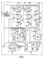
- Referring to Fig. 1, an NPN
bipolar transistor 17 and an NPNbipolar transistor 18 are connected in series between a high power source Vcc and the ground. A collector of thebipolar transistor 17 is connected to the high power source Vcc, an emitter being connected to collector of thetransistor 18 and anoutput terminal 12. An emitter of thetransistor 18 is connected to the ground. - A P-
channel MOS transistor 13 and an N-channel MOS transistor 14 are connected in series between a low power source V'cc which is lower than the high power source Vcc and the ground, each gate of theseMOS transistor input terminal 11. A source of the P-channel MOS transistor 13 is connected to the lower power source V'cc, a drain being connected to a base of theNPN transistor 17 and a drain of the N-channel MOS transistor 14. A source of the N-channel MOS transistor 14 is connected to the ground. A drain of an N-channel MOS transistor 15 is connected to theoutput terminal 12, a gate being connected to theinput terminal 11 and a source being connected not only to the ground through aresistor 16 but also to a base of theNPN transistor 18. - In the steady state when the
output terminal 11 is at a high level, the N-channel MOS transistors NPN transistor 18 are on, the P-channel MOS transistor 13 and theNPN transistor 17 being off to make theoutput terminal 12 be at a low level. When theinput terminal 11 is at a low level, the N-channel MOS transistors NPN transistor 18 are off, the P-channel MOS transistor 13 and theNPN transistor 17 being on to make theoutput terminal 12 be at a high level. Therefore, theNPN transistors - When the
input terminal 11 is changed from the high level to the low level, the N-channel MOS transistor 15 turns off and the charges stored in the base of theNPN transistor 18 are discharged quickly through theresistor 16. Therefore, theNPN transistor 18 turns off quickly to make all the current from theNPN transistor 17 flow into the load (not shown) connected to theoutput terminal 12. On the other hand, the P-channel MOS transistor 13 turns on to make the N-channel MOS transistor 14 turn off, causing theNPN transistor 17 to turn on quickly. As a result, a high level signal is produced at theoutput terminal 12. - According to this first embodiment of Fig. 1, the source of the P-
channel MOS transistor 13 is connected to the low power source V'cc (which is lower than the high power source Vcc) and thus the high level voltage at theoutput terminal 12 becomes V'cc - VBE (where VBE is the built-in voltage between the base and emitter of the NPN transistor 17), resulting in the small change from "on" state to "off" state at theoutput terminal 12. Here, since a power is consumed in proportional to the square of the voltage change, the power consumption at the transient time becomes small. Moreover, since the collector of theNPN transistor 17 is connected to the high power source VCC which is higher than the low power source V'cc, the collector-emitter saturation voltage VCE sat. of theNPN transistor 17 remains large. Accordingly, the cut-off frequency fT keeps high and a large collector current IC may be supplied, resulting in a high speed operation and a large driving ability. - When the input terminal is changed from the low level to the high level, the P-
channel transistor 13 turns off, the N-channel MOS transistor 14 turning on to quickly discharge charges stored in the base of theNPN transistor 17 through the N-channel MOS transistor 14, resulting in an "off" state of theNPN transistor 17. The N-channel MOS transistor 15 turns on and a part of the current flowing through the N-channel MOS transistor 15 to the ground is bypassed through the base of theNPN transistor 18 to turn on theNPN transistor 18 quickly. Accordingly, theoutput terminal 12 is changed from a high level to a low level. - As described above, the charges stored in the base of the
NPN transistor 17 and theNPN transistor 18 during their "on" states are discharged quickly by the N-channel transistor 14 and theresistor 16, respectively. TheNPN transistor 18 is quickly turned on by the N-channel transistor 15 and theresistor 16. Consequently, the current flowing through both theNPN transistor 17 and theNPN transistor 18 at the transient time is suppressed and the power consumption at the transient time is remarkably reduced. - The high power source Vcc is favorably supplied from outside the chip, the voltage of the high power source Vcc being ordinarily 5 V. The low power source V'cc is favorably supplied by converting the voltage supplied from the high power source Vcc with use of an internal voltage converter or a voltage regulator to a voltage of 3.3 V, ordinarily. In a case of 3.3 V of the low power supply V'cc, since the base-emitter built-in voltage VBE is about 0.7 V, the high level at the
output terminal 12 is about 2.6 V. The voltage of low power supply V'cc may be 4.0 V to raise the high level at theoutput terminal 12 to 3.3 V. - Referring to Fig. 2, a P-
channel MOS transistor 23 and an N-channel MOS transistor 24 are connected in series between the power source V'cc and the ground. A source of the P-channel MOS transistor 23 is connected to the power source V'cc, a drain of the P-channel transistor 23 being connected to both a drain of the N-channel transistor 24 and the gates of theMOS transistors channel MOS transistor 24 is connected to the ground. - A register 21 and an NPN
bipolar transistor 22 are connected in series between the high power source Vcc (which is higher than the low power source V'cc) and the ground. A collector of theNPN transistor 22 is connected not only to the high power source Vcc through the resistor 21 but also to the gates of theMOS transistors NPN transistor 22 is connected to theinput terminal 11, the emitter being connected to the ground. The circuit composed of theMOS transistors resistor 16 and theNPN transistors - When the
input terminal 11 is changed to the high level, theNPN transistor 22 turns on to make the potential of its collector at the low level. Accordingly, the P-channel MOS transistor 23 turns on, the N-channel MOS transistor 24 turning off to raise the gate potential of theMOS transistors - When the
input terminal 11 is changed to the low level, theNPN transistor 22 turns off to make the potential of its collector at the high level. Accordingly, the P-channel MOS transistor 23 turns off, the N-channel MOS transistor turning on, resulting in making the gate potential of theMOS transistors - Therefore, the gates of the
MOS transistors input terminal 11 of high level, the gates of theMOS transistors input terminal 11 of low level. The change in amplitude from the low level to the high level at the gates of theseMOS transistors MOS transistors - Consequently, since the
output terminal 12 swings between the voltage of the low power source V'cc which supplies a voltage lower than the high power source Vcc and the ground, the inverter consuming a low power can be obtained. - Referring to Fig. 3, a NAND circuit having two
input terminals bipolar transistor 17 and the NPNbipolar transistor 18 are connected in series between the power source Vcc and the ground, the collector of the NPNbipolar transistor 17 being connected to Vcc, the emitter of theNPN transistor 17 being connected to both theoutput terminal 12 and the collector of theNPN transistor 18 and the emitter of theNPN transistor 18 being connected to the ground. - A P-
channel MOS transistors transistors transistors NPN transistor 17, a gate of the P-channel MOS transistor 13a being connected to aninput terminal 11a and a gate of the P-channel MOS transistor 13b being connected to aninput terminal 11b. - N-
channel MOS transistors channel MOS transistor 14a being connected to the drains of the P-channel MOS transistors NPN transistor 17, a source of the N-channel MOS transistor 14a being connected a drain of the N-channel MOS transistor 14b, a source of the N-channel MOS transistor 14b being connected to the ground, a gate of the N-channel MOS transistor 14a being connected to the gate of the P-channel MOS transistor 13a and theinput terminal 11a and a gate of the N-channel MOS transistor 14b being connected to the gate of the P-channel MOS transistor 13b and theinput terminal 11b. - An N-
channel MOS transistor 15a and an N-channel MOS transistor 15b is connected in series, a drain of the N-channel MOS transistor 15a being connected to theoutput terminal 12, the emitter of theNPN transistor 17 and the collector of theNPN transistor 18, a source of the N-channel MOS transistor 15a being connected to a drain of the N-channel MOS transistor 15b, a source of the N-channel MOS transistor 15b being connected to the ground by theresistor 16 and also connected to the base of theNPN transistor 18, a gate of the N-channel MOS transistor 15a being connected to the gate of the P-channel MOS transistor 13a, the gate of the N-channel MOS transistor 14a and theinput terminal 11a and a gate of the N-channel MOS transistor 15b being connected to the gate of the P-channel MOS transistor 13b, the gate of the N-channel MOS transistor 14b and theinput terminal 11b. - When at least one of the two
input terminal channel MOS transistors channel MOS transistors transistors NPN transistor 17 is charged quickly by the P-channel MOS transistors output terminal 12. At least one of the N-channel MOS transistors NPN transistor 18 turns off by discharging the charges stored in the base of thistransistor 18 through theresistor 16. - When both the
input terminals channel MOS transistors channel MOS transistors NPN transistor 17 are discharged through thetransistors channel MOS transistors NPN transistor 18 through these N-channel MOS transistors output terminal 12 is quickly changed to the low level. - As described above, since the charges are charged into or discharged from the bases of the NPN
bipolar transistors bipolar transistors - Moreover, since the sources of the P-
channel transistors output terminal 12 is V'cc - VBE, resulting in the small change in output level from the low level to the high level. Accordingly, the power consumption at the transient time becomes small. Furthermore, the collector of theNPN transistor 17 is connected to the high power source Vcc which is higher than the low power source V'cc and theNPN transistor 17 operates at a high speed with large driving ability as same as the inverter shown in Fig. 1. - Referring to Fig. 4, the
resistor 16 in the inverter shown in Fig. 1 is replaced by an N-channel MOS transistor 25. The circuit operation is similar to the inverter shown in Fig. 1. The switching speed of this inverter is smaller than the inverter with theresistor 16 such as shown in Fig. 1, but the pattern layout is more simple than the inverter having theresistor 16 such as shown in Fig. 1. - Referring to Fig. 5, the N-
channel MOS transistor 13 in the inverter shown in Fig. 1 is replaced by a resistor 33. Referring to Fig. 6, the N-channel MOS transistor 13 in the inverter shown in Fig. 1 is replaced by aload MOS transistor 43. The base current always flows into the base of theNPN transistor 17 through the resistor 33 or theload MOS transistor 43 and the current flows from the power source V'cc to the ground. However, when the frequency of the signal applied to theinput terminal 11 is high, for example, when higher than 100 MHz, the increase in the power consumption based on this constant base current is negligible. - In the inverter shown in Fig. 1, the high level at the
output terminal 12 is V'cc - VBE. Since V'cc is ordinarily chosen as 3.3 V and the built-in voltage VBE is about 0.7 V, the high level at theoutput terminal 12 is 2.6 V. Additionally, the base-emitter saturation voltage VBE of theNPN transistor 18 is about 0.7 V and the low level at theoutput terminal 12 is determined by the base-emitter built-in voltage VBE of 0.7 V due to the "on" of the N-channel MOS transistor 15. Therefore, the change in output level from the low level to the high level at theoutput terminal 12 becomes as small as 1.9 V and then a noise margin becomes small. In this embodiment, in order to lower the low level at theoutput terminal 12 to the ground level, the switching element constructed with the N-channel transistor 15,resistor 16 and the NPNbipolar transistor 18 is replaced in a 6th embodiment shown in Fig. 7 by an N-channel MOS transistors 51. - A P-
channel MOS transistor 13 and an N-channel MOS transistor 14 are connected in series to form a CMOS inverter, a source of the P-channel MOS transistor 13 being connected to a low power source V'cc which supplies a voltage lower than the high power source Vcc, a gate of the P-channel MOS transistor 13 being connected to theinput terminal 11, a drain of the P-channel MOS transistor 13 being connected to a drain of the N-channel MOS transistor 14, a gate of the N-channel MOS transistor 14 being connected to the gate of the P-channel MOS transistor 13 and theinput terminal 11 and a source of the N-channel MOS transistor 14 being connected to the ground. The NPNbipolar transistor 17 and an N-channel MOS transistor 51 are connected in series between the high power source Vcc and the ground, the collector of theNPN transistor 17 being connected to the high power source Vcc, the base of theNPN transistor 17 being connected to both the drains of theMOS transistors NPN transistor 17 being connected to theoutput terminal 12 and a drain of the N-channel MOS transistor 51, a source of the N-channel MOS transistor being connected to the ground and a gate of the N-channel MOS transistor 51 being connected to theinput terminal 11 and the gates of theMOS transistors - In a steady state when the
input terminal 11 is at the high level, the P-channel MOS transistor 13 and theNPN transistor 17 remain "off" states, both the N-channel MOS transistor output terminal 12 being at a low level. When theinput terminal 11 is at the low level, the P-channel MOS transistor 13 and the NPNbipolar transistor 17 are "on" state, both the N-channel MOS transistor output terminal 12 being at a high level. Therefore, in the steady state, theNPN transistor 17 and the N-channel MOS transistor 51 are not simultaneously in the "on" states not to consume a power in the steady state. - When the
input terminal 11 is changed from the high level to the low level, the P-channel MOS transistor 13 turns on, the N-channel MOS transistors channel MOS transistor 13 flows into the base of theNPN transistor 17 to turn thetransistor 17 on quickly, resulting in a high level at theoutput terminal 12. - When the
input terminal 11 is changed from the low level to the high level, the P-channel MOS transistor 13 turns off, both the N-channel MOS transistors NPN transistor 17 are discharged quickly through the N-channel MOS transistor 14. Consequently, theNPN transistor 17 turns off quickly to make theoutput terminal 12 at a low level. - Since the source of the P-
channel MOS transistor 13 is connected to the low power source V'cc (which is lower than the high power source Vcc), the high level at theoutput terminal 12 is V'cc - VBE, resulting in the small change in output level at theoutput terminal 12 from the low level to the high level. Therefore, the power consumption at the transient time is small. Using the N-channel MOS transistor 51 in place of thebipolar transistor 18 in Fig. 1, the low level at theoutput terminal 12 is lowered to the ground. Accordingly, a large noise margin can be obtained although the high level at theoutput terminal 12 is lowered to V'cc - VBE. Furthermore, the collector of theNPN transistor 17 is connected to the high power source Vcc which is higher than the low power source V'cc, resulting in a high speed operation and a large driving ability. - Referring to Fig. 8, a NAND circuit having two
input terminals bipolar transistor 17 and the N-channel MOS transistors NPN transistor 17 being connected to the high power source Vcc, an emitter of theNPN transistor 17 being connected to theoutput terminal 12 and a drain of the N-channel MOS transistor 51a, a gate of the N-channel MOS transistor 51a being connected to theinput terminal 11a, a source of the N-channel MOS transistor 51a being connected to a drain of the N-channel MOS transistor 51b, a gate of the N-channel MOS transistor 51b being connected to theinput terminal 11b and a source of the N-channel MOS transistor 51b being connected to the ground. - A P-
channel MOS transistors transistors transistors NPN transistor 17, a gate of the P-channel MOS transistor 13a being connected to theinput terminal 11a and a gate of the P-channel transistor 13b being connected to theinput terminal 11b. - N-
channel MOS transistors channel MOS transistor 14a being connected to the drains of the P-channel transistors transistor 17, a source of the N-channel MOS transistor 14a being connected to a drain of the N-channel MOS transistor 14b, a gate of the N-channel MOS transistor 14a being connected to theinput terminal 11a, a gate of the N-channel MOS transistor 14b being connected to theinput terminal 11b and a source of the N-channel MOS transistor 14b being connected to the ground. - When at least one of the two
input terminals channel MOS transistor channel MOS transistors channel MOS transistors NPN transistor 17 is charged quickly through the P-channel MOS transistors output terminal 12. - When both the
input terminal channel MOS transistors channel MOS transistors channel MOS transistors NPN transistor 17 are discharged through the N-channel MOS transistors output terminal 12. - Since the sources of the P-
channel MOS transistors output terminal 12 is as small as V'cc - VBE, resulting in a low power consumption. Using the N-channel MOS transistors output terminal 12 is lowered to the ground. Therefore, a large noise margin can be maintained. Moreover, since the collector of theNPN transistor 17 is connected to the high power source Vcc, the NAND circuit can be operated at high speed with large driving ability. - Referring to Fig. 9, a NOR circuit having two
input terminals channel transistors bipolar transistor 17 are connected in series between the high power source Vcc and the ground, a collector of theNPN transistor 17 being connected to the high power source Vcc, an emitter of theNPN transistor 17 being connected to theoutput terminal 12 and both drains of the N-channel MOS transistors channel MOS transistors channel MOS transistor 51c being connected to theinput terminal 11a and a gate of the N-channel MOS transistor 51d being connected to theinput terminal 11b. - P-
channel MOS transistors 13c and 13d are connected in series, a source of the P-channel MOS transistor 13c being connected to the low power source V'cc which is lower than the high power source Vcc, a drain of the P-channel MOS transistor 13c being connected to a source of the P-channel MOS transistor 13d, a drain of the P-channel MOS transistor 13d being connected to the base of theNPN transistor 17, a gate of the P-channel MOS transistor 13c being connected to theinput terminal 11a and a gate of the P-channel MOS transistor 13d being connected to theinput terminal 11b. - N-
channel MOS transistors MOS transistors channel MOS transistor 13d and the base of theNPN transistor 17, both sources of the N-channel MOS transistors channel MOS transistor 14c being connected to theinput terminal 11a and a gate of the N-channel MOS transistor 14d being connected to theinput terminal 11b. - When at least one of the
input terminals channel MOS transistors 13c and 13d turns off, at least one of the N-channel MOS transistors channel MOS transistors NPN transistor 17 is discharged quickly by the N-channel MOS transistors output terminal 12. - When both the
input terminal channel MOS transistors 13c and 13d turn on, both the N-channel MOS transistors channel MOS transistors NPN transistor 17 is charged quickly by the P-channel MOS transistors 13c and 13d, resulting in the high level at theoutput terminal 12. - The sources of the P-channel MOS transistor 13c being connected to the low power source V'cc, the high level at the
output terminal 12 is as small as V'cc - VBE, resulting in the low power consumption during a transient period followed after an input change. Using the N-channel MOS transistors output terminal 12 is lowered to the ground. Therefore, a large noise margin can be similarly maintained. Moreover, since the collector of theNPN transistor 17 is connected to the high power source Vcc, the NOR circuit can be operated at high speed with large driving ability. - Referring to Fig. 10, on a semiconductor pellet 190 a logic IC is constructed with an external
power supply terminal 101, asignal input terminal 102, asignal output terminal 101, avoltage converter 103 which converts the external power voltage of, for example, 5 V to an internal power voltage of, for example, 3.3 V, aBi-CMOS circuit 104 havinginternal gate circuits output buffer 130 and a data-bus driver 140,Bi-CMOS circuits CMOS circuit 160 having P-channel MOS transistors channel MOS transistors power supply terminal 101, alevel shift circuit 170 and aCMOS circuit 180 having a P-channel MOS transistors channel MOS transistors voltage converter 103. - The internal gates 120 (120′) has two
input terminals 121a (121a′) and 121b (121b′), two P-channel MOS transistors 123a (123a′) and 123b (123b′), four N-channel MOS transistors 124a (124a′), 124b (124b′), 125a (125a′) and 125b (125b′), two NPN bipolar transistors 127 (127′) and 128 (128′), a resistor 126 (126′) and an output terminal 122 (122′). The sources of the P-channel MOS transistors voltage converter 103. The collector of the NPNbipolar transistor 127 is connected to the externalpower supply terminal 101. This internal gate is the same NAND circuit as the one shown in Fig. 3. - The
output buffer 130 is the inverter as shown in Fig. 1, thebuffer 130 having a P-channel MOS transistor 133, N-channel MOS transistors resistor 136 andNPN transistors channel MOS transistor 133 being connected to the output of thevoltage converter 103 and the collector of theNPN transistor 137 being connected to the externalpower supply terminal 101. The data-bus driver 140 is the inverter as shown in Fig. 1, thedriver 140 having a P-channel MOS transistor 143, N-channel MOS transistors resistor 146 andNPN transistors 147 and 148, the source of the P-channel MOS transistor 143 being connected to the output of thevoltage converter 103 and the collector of theNPN transistor 147 being connected to the externalpower supply terminal 101. The signals processed in theBi-CMOS circuit 104 is outputted to theoutput terminal 110 by theoutput buffer 130. By the data-bus buffer 140, other signals are outputted from theoutput terminal 122′ of theinternal gate 120′ to theinput terminal Bi-CMOS circuit MOS transistors 181˝and 182˝ of theCMOS circuit 180 through the data-bus 113 having theparasitic capacitors - The CMOS circuit 150 (150′) also has the inverter as shown in Fig. 1. This inverter has a P-channel MOS transistors 153 (153′), N-channel MOS transistors 154 (154′) and 155 (155′), a register 156 (156′) and the NPN transistors 157 (157′) and 158 (158′), the source of the P-channel MOS transistor 153 (153′) being connected to the output of the
voltage converter 103 and the collector of the NPN transistor 157 (157′) being connected to the externalpower supply terminal 101. - In the
Bi-CMOS circuits 104 and 150 (150′), since the power for the CMOS circuits is supplied by thevoltage converter 103 which converts the external power voltage of 5 V to the internal power voltage of 3.3 V, the logic amplitude in theBi-CMOS circuits power supply terminal 101, the cut-off frequency fT is held at high and the collector current IC is large, resulting in a high speed operation and the large driving ability. Moreover, even if theinternal gates output buffer 130 and the data-bus driver 140 are switched simultaneously, thevoltage converter 103 which supplies the power to the CMOS circuit without supplying the power to the bipolar circuit does not show the instability. - Referring to Fig. 11, a DRAM circuit is constructed with
address input terminals decoders word line drivers BL , word lines WL1, WL2, memory cells with N-channel MOS transistors precharge circuit 205. Referring to Fig. 12, the wordline driver circuit 204 is constructed with the inverter shown in Fig. 4. The collector of theNPN transistor 17 is connected to an external power source Vcc of 5 V, the source of the P-channel MOS transistor 13 being connected to an internal power source V'cc of 3.3 V supplied by an internal power converter. The emitter of theNPN transistor 18 is connected to an power source of -VBE to make the low logic level at theoutput terminal 12 0 V. - Referring to Fig. 13, a SRAM circuit is constructed with an
address input terminal 301, anaddress buffer 302,decoders word line drivers memory cells BL . - Referring to Fig. 14, the
word line driver 304 is constructed with the inverter shown in Fig. 4. - The collector of the
NPN transistor 17 is connected to anexternal power source 308 of 5 V, the source of the P-channel MOS transistor 13 being connected to aninternal power source 307 of 3.3 V supplied by an internal power converter (not shown). Since the emitter of theNPN transistor 18 is connected to the ground, the low level at theoutput terminal 12 of this inverter is higher than the ground potential by the base-emitter built-in potential VBE of about 0.7 V. Thememory cell 311 is constructed with N-channel MOS transistors resistors resistors internal power source 307 of 3.3 V. - Referring to Fig. 15, the
word line driver 304 is constructed with the inverter shown in Fig. 7. The collector of theNPN transistor 17 is connected to theexternal power source 308 of 5 V, the source of the P-channel MOS transistor 13 is connected to theinternal power source 307 of 3.3 V supplied by an internal power converter (not shown). Since the N-channel MOS transistor 51 is used in place of theNPN transistor 18 shown in Fig. 14, the low level at theoutput terminal 12 is lowered to the ground level, resulting in a large logic amplitude from the low level to the high level at theoutput terminal 12.
Claims (18)
an input terminal;
an output terminal;
a first power voltage line held at a first power voltage;
a second power voltage line held at a second power voltage lower than said first power voltage;
a reference voltage line;
a field effect transistor having a gate connected to said input terminal, one of a source and a drain connected to said reference voltage line and the other of the source and the drain;
a bipolar output transistor having a collector connected to said first power voltage line, an emitter connected to said output terminal and a base;
a load element having a first terminal connected to said other of the source and the drain of said field effect transistor and the base of said bipolar output transistor and a second terminal connected to said second power voltage line; and
a switching element having a control electrode connected to said input terminal and the gate of said field effect transistor, a third terminal connected to said reference voltage line and a fourth terminal connected to the emitter of said bipolar transistor and said output terminal, said switching element connecting said third terminal to said fourth terminal when a first level of an input signal turning said field effect transistor on is inputted to said input terminal and disconnecting said third terminal from said fourth terminal when a second level of said input signal turning said field effect transistor off is inputted to said input terminal.
a first additional P-channel MOS transistor having a gate, one of a source and a drain connected to said second power voltage line and the other of the source and the drain connected to the gate of said P-channel MOS transistor, said N-channel MOS transistor and said first additional N-channel MOS transistor;
a third additional N-channel MOS transistor having a gate connected to the gate of said first additional P-channel MOS transistor, one of a source and a drain connected to the other of the source and the drain of said first additional P-channel MOS transistor and the gates of said P-channel MOS transistor, said N-channel MOS transistor and said first additional N-channel MOS transistor and the other of the source and the drain connected to said reference voltage line;
a second additional resistor; and
a second additional NPN bipolar transistor having an emitter connected to said reference voltage line, a base connected to said input terminal and a collector connected to the gates of said first additional P-channel MOS transistor and said third additional N-channel MOS transistor and to said first power voltage line through said second additional resistor.
a first additional input terminal;
a second additonal P-channel MOS transistor having a gate connected to said first additional input terminal, one of a source and a drain connected to said second power voltage line and the other of the source and the drain connected to the base of said NPN bipolar transistor, the other of the source and the drain of said P-channel MOS transistor and the other of the source and the drain of said N-channel MOS transistor;
a fourth additional N-channel MOS transistor connected between said one of the source and the drain of said N-channel MOS transistor and said reference voltage line and having a gate connected to said first additional input terminal and the gate of said second additional P-channel MOS transistor;
a fifth additional N-channel MOS transistor connected between said first additional N-channel MOS transistor and the connecting point between said first additional resistor and the base of said first additional NPN bipolar transistor and having a gate connected to said first additional input terminal and the gates of said second additional P-channel MOS transistor and said fourth additional N-channel MOS transistor.
a second additonal input terminal;
a third additional P-channel MOS transistor having a gate connected to said second additional input terminal, one of a source and a drain connected to said second power voltage line and the other of the source and the drain connected to the base of said NPN bipolar transistor, the other of the source and the drain of said P-channel MOS transistor and the other of the source and the drain of said N-channel MOS transistor;
a sixth additional N-channel MOS transistor connected between said N-channel MOS transistor and said reference voltage line and having a gate connected to said second additional input terminal and the gate of said third additional P-channel MOS transistor; and
a seventh additional N-channel MOS transistor connected between said another N-channel MOS transistor and said reference voltage line and having a gate connected to said second additional input terminal and the gates of said third additional P-channel MOS transistor and said sixth additional N-channel MOS transistor.
a third additional input terminal;
a fourth additional P-channel MOS transistor connected between said P-channel MOS transistor and the connecting point of the base of said NPN bipolar transistor and the other of the source and the drain of said N-channel MOS transistor and having a gate connecting to said third additional input terminal;
an eighth additional N-channel MOS transistor having a gate connected to said third additional input terminal and the gate of said fourth additional P-channel MOS transistor, one of a source and a drain connected to the base of said NPN bipolar transistor and the other of the source and the drain of said fourth additional P-channel MOS transistor and the other of the source and the drain of said N-channel MOS transistor and the other of the source and the drain connected to said reference voltage line; and
a ninth additional N-channel MOS transistor having a gate connected to said third additional input terminal and the gates of said fourth additional P-channel MOS transistor and said eighth additional N-channel MOS transistor, one of a source and a drain connected to said output terminal, the emitter of said NPN bipolar transistor and the one of the source and the drain of said another N-channel MOS transistor and the other of the source and the drain connected to said reference voltage line.
a first input terminal;
a second input terminal;
an output terminal;
a first fixed potential source;
a second fixed potential source supplying a potential higher than said first fixed potential source;
a third fixed potential source having another potential between said first fixed potential and said second fixed potential;
a first NPN bipolar transistor and a second NPN bipolar transistor in series between said first fixed potential source and said second fixed potential source, a collector of said first NPN bipolar transistor being connected to said second fixed potential source, an emitter of said first NPN transistor and a collector of said second NPN transistor being connected to said output terminal and a emitter of said second NPN transistor being connected to said first fixed potential source;
a first P-channel MOS transistor and a second P-channel MOS transistor connected in parallel between said third fixed potential source and a base of said first NPN bipolar transistor, one of a source and a drain of said first P-channel MOS transistor and one of a source and a drain of said second P-channel MOS transistor being connected to said third fixed potential source, the other of the source and the drain of said first P-channel MOS transistor and the other of the source and the drain of said second P-channel MOS transistor being connected to the base of said first NPN bipolar transistor, a gate of said first P-channel MOS transistor being connected to said first input terminal and a gate of said second P-channel MOS transistor being connected to said second input terminal;
a first N-channel MOS transistor and a second N-channel MOS transistor connected is series between said first fixed potential source and the base of said first NPN bipolar transistor, one of a source and a drain of said first N-channel MOS transistor being connected to the base of said first NPN transistor, the other of the source and the drain of said first P-channel MOS transistor and the other of the source and the drain of said second P-channel MOS transistor, the other of the source and the drain of said first N-channel MOS transistor being connected to one of a source and a drain of said second N-channel MOS transistor, the other of the source and the drain being connected to said first fixed potential source, a gate of said first N-channel MOS transistor being connected to said first input terminal and the gate of said first P-channel MOS transistor and a gate of said second N-channel MOS transistor being connected to said second input terminal and the gate of said second P-channel MOS transistor;
a resistor; and
a third N-channel MOS transistor and a fourth N-channel MOS transistor connected in series between said output terminal and the base of said second NPN bipolar transistor, one of a source and a drain of said third N-channel MOS transistor being connected to said output terminal, the emitter of said first NPN transistor and the collector of said second NPN transistor, the other of the source and the drain of said third N-channel MOS transistor being connected to one of a source and a drain of said fourth N-channel MOS transistor, the other of the source and the drain of said fourth N-channel MOS transistor being connected to said first fixed potential source through said resistor and to the base of said second NPN bipolar transistor, a gate of said third N-channel MOS transistor being connected to said first input terminal, the gate of said first P-channel MOS transistor and the gate of said first N-channel MOS transistor and a gate of said fourth N-channel MOS transistor being connected to said second input terminal, the gate of said second P-channel MOS transistor and the gate of said second N-channel MOS transistor.
a first input terminal;
a second input terminal;
an output terminal;
a first fixed potential source;
a second fixed potential source supplying a potential higher than said first fixed potential source;
a third fixed potential source supplying another potential between said first fixed potential source and said second fixed potential source;
an NPN bipolar transistor having a collector connected to said second fixed potential source, an emitter connected to said output terminal and a base;
a first N-channel MOS transistor and a second N-channel MOS transistor connected in series between said output terminal and said first fixed potential source, one of a source and a drain of said first N-channel MOS transistor being connected to said output terminal and the emitter of said NPN bipolar transistor, the other of the source and the drain of said first N-channel MOS transistor being connected to one of a source and a drain of said second N-channel MOS transistor, the other of the source and the drain of said second N-channel MOS transistor being connected to said first fixed potential source, a gate of said first N-channel MOS transistor being connected to said first input terminal and a gate of said second N-channel MOS transistor being connected to said second input terminal;
a first P-channel MOS transistor and a second P-channel MOS transistor connected in parallel between said third fixed potential source and the base of said NPN transistor, one of a source and a drain of said first P-channel MOS transistor and one of a source and a drain of said second P-channel MOS transistor being connected to said third fixed potential source, the other of the source and the drain of said first P-channel MOS transistor and the other of the source and the drain of said second P-channel MOS transistor being connected to the base of said NPN bipolar transistor, a gate of said first P-channel MOS transistor being connected to said first input terminal and the gate of said first N-channel MOS transistor and a gate of said second P-channel MOS transistor being connected to said second input terminal and the gate of said second N-channel MOS transistor; and
a third N-channel MOS transistor and a fourth N-channel MOS transistor being connected in series between the base of said NPN transistor and said first fixed potential source, one of a source and a drain of said third N-channel MOS transistor being connected to the base of said NPN transistor, the other of the source and the drain of said first P-channel MOS transistor and the other of the source and the drain of said second P-channel MOS transistor, the other of the source and the drain of said third N-channel MOS transistor being connected to one of a source and a drain of said fourth N-channel MOS transistor, the other of the source and the drain of said fourth N-channel MOS transistor being connected to said first fixed potential source, a gate of said third MOS transistor being connected to said first input terminal, the gate of said first N-channel MOS transistor and the gate of said first P-channel MOS transistor and a gate of said fourth N-channel MOS transistor being connected to said second input terminal, the gate of said second N-channel MOS transistor and the gate of said second P-channel MOS transistor.
a first input terminal;
a second input terminal;
an output terminal
a first fixed potential source;
a second fixed potential source supplying a potential higher than said first fixed potential source;
a third fixed potential source supplying another potential between said first fixed potential source and said second fixed potential source;
an NPN bipolar transistor having a collector connected to said second fixed potential source, an emitter connected to said output terminal and a base;
a first N-channel MOS transistor and a second N-channel MOS transistor connected in parallel between said output terminal and said first fixed potential source, one of a source and a drain of said first N-channel MOS transistor and one of a source and a drain of said second N-channel MOS transistor being connected to said output terminal and the emitter of said NPN transistor, the other of the source and the drain of said first N-channel MOS transistor and the other of the source and the drain of said second N-channel MOS transistor being connected to said first fixed potential source, a gate of said first N-channel MOS transistor being connected to said first input terminal and a gate of said second N-channel MOS transistor being connected to said second input terminal;
a first P-channel MOS transistor and a second P-channel MOS transistor connected between said third fixed potential source and the base of said NPN transistor, one of a source and a drain being connected to said third fixed potential source, the other of the source and the drain of said first P-channel MOS transistor being connected to one of a source and a drain of said second P-channel MOS transistor, the other of the source and the drain of said second P-channel MOS transistor being connected to the base of said NPN bipolar transistor, a gate of said first P-channel MOS transistor being connected to said first input terminal and the gate of said first N-channel MOS transistor and a gate of said second P-channel MOS transistor being connected said second input terminal and the gate of said second N-channel MOS transistor; and
a third N-channel MOS transistor and a fourth N-channel MOS transistor connected in parallel between the base of said NPN transistor and said first fixed potential source, one of a source and a drain of said third N-channel MOS transistor and one of a source and a drain of said fourth N-channel MOS transistor being connected to the base of said NPN bipolar transistor and the other of the source and the drain of said second P-channel MOS transistor, the other of the source and the drain of said third N-channel MOS transistor and the other of the source and the drain of said fourth N-channel MOS transistor being connected to said first fixed potential source, a gate of said third N-channel MOS transistor being connected to said first input terminal, the gate of said first N-channel MOS transistor and the gate of said first N-channel MOS transistor and a gate of said fourth N-channel MOS transistor being connected to said second input terminal, the gate of said second P-channel MOS transistor and the gate of said second N-channel MOS transistor.
a semiconductor chip;
an external power supply terminal formed on said semiconductor chip to which an external power of a first voltage is supplied from outside said semiconductor chip;
an internal voltage converter which converts said first voltage to a second voltage lower than said first voltage;
a MOS circuit operated with said second voltage and outputting a signal of said second voltage; and
a bipolar transistor having a collector connected to said external power supply terminal and a base which receives said signal of said second voltage from said MOS circuit.
Applications Claiming Priority (4)
| Application Number | Priority Date | Filing Date | Title |
|---|---|---|---|
| JP62203156A JPS6447124A (en) | 1987-08-17 | 1987-08-17 | Inverter circuit |
| JP203156/87 | 1987-08-17 | ||
| JP63020278A JPH01194711A (en) | 1988-01-29 | 1988-01-29 | Inverter circuit |
| JP20278/88 | 1988-01-29 |
Publications (3)
| Publication Number | Publication Date |
|---|---|
| EP0304035A2 true EP0304035A2 (en) | 1989-02-22 |
| EP0304035A3 EP0304035A3 (en) | 1989-07-12 |
| EP0304035B1 EP0304035B1 (en) | 1993-02-10 |
Family
ID=26357190
Family Applications (1)
| Application Number | Title | Priority Date | Filing Date |
|---|---|---|---|
| EP88113356A Expired - Lifetime EP0304035B1 (en) | 1987-08-17 | 1988-08-17 | Bi-mos circuit capable of high speed operation with low power consumption |
Country Status (3)
| Country | Link |
|---|---|
| US (1) | US4926069A (en) |
| EP (1) | EP0304035B1 (en) |
| DE (1) | DE3878345T2 (en) |
Cited By (5)
| Publication number | Priority date | Publication date | Assignee | Title |
|---|---|---|---|---|
| EP0383289A1 (en) * | 1989-02-17 | 1990-08-22 | Texas Instruments Deutschland Gmbh | Integrated push-pull output stage |
| EP0398808A2 (en) * | 1989-05-17 | 1990-11-22 | Fujitsu Limited | Level conversion circuit for converting elc-level signal into ttl-level signal |
| EP0403075A2 (en) * | 1989-05-15 | 1990-12-19 | Texas Instruments Incorporated | High performance bicmos logic circuit with full output voltage swing |
| EP0410885A2 (en) * | 1989-07-25 | 1991-01-30 | Fujitsu Limited | Level-conversion semiconductor device |
| DE102009001966A1 (en) | 2009-03-30 | 2010-10-07 | Evonik Röhm Gmbh | Coating composition, (meth) acrylic polymer and monomer mixture for producing the (meth) acrylic polymer |
Families Citing this family (16)
| Publication number | Priority date | Publication date | Assignee | Title |
|---|---|---|---|---|
| JP2550138B2 (en) * | 1988-03-18 | 1996-11-06 | 株式会社日立製作所 | Semiconductor integrated circuit device having bipolar transistor and field effect transistor |
| JPH0239719A (en) * | 1988-07-29 | 1990-02-08 | Fujitsu Ltd | Semiconductor circuit |
| JPH07120937B2 (en) * | 1988-11-08 | 1995-12-20 | 日本電気株式会社 | Inverter circuit |
| EP0387461A1 (en) * | 1989-03-14 | 1990-09-19 | International Business Machines Corporation | Improved BICMOS logic circuit with full swing operation |
| US5063304A (en) * | 1990-04-27 | 1991-11-05 | Texas Instruments Incorporated | Integrated circuit with improved on-chip power supply control |
| US5140191A (en) * | 1990-11-05 | 1992-08-18 | Molorola, Inc. | Low di/dt BiCMOS output buffer with improved speed |
| JP2570492B2 (en) * | 1990-11-28 | 1997-01-08 | 日本電気株式会社 | Semiconductor circuit |
| JP3079515B2 (en) * | 1991-01-29 | 2000-08-21 | 株式会社東芝 | Gate array device, input circuit, output circuit, and step-down circuit |
| US5132567A (en) * | 1991-04-18 | 1992-07-21 | International Business Machines Corporation | Low threshold BiCMOS circuit |
| US5118972A (en) * | 1991-06-13 | 1992-06-02 | International Business Machines Corporation | BiCMOS gate pull-down circuit |
| US5994755A (en) | 1991-10-30 | 1999-11-30 | Intersil Corporation | Analog-to-digital converter and method of fabrication |
| US5369309A (en) * | 1991-10-30 | 1994-11-29 | Harris Corporation | Analog-to-digital converter and method of fabrication |
| US5254891A (en) * | 1992-04-20 | 1993-10-19 | International Business Machines Corporation | BICMOS ECL circuit suitable for delay regulation |
| US6002268A (en) * | 1993-01-08 | 1999-12-14 | Dynachip Corporation | FPGA with conductors segmented by active repeaters |
| US5355035A (en) * | 1993-01-08 | 1994-10-11 | Vora Madhukar B | High speed BICMOS switches and multiplexers |
| US5552724A (en) * | 1993-09-17 | 1996-09-03 | Texas Instruments Incorporated | Power-down reference circuit for ECL gate circuitry |
Citations (3)
| Publication number | Priority date | Publication date | Assignee | Title |
|---|---|---|---|---|
| EP0132822A2 (en) * | 1983-07-25 | 1985-02-13 | Hitachi, Ltd. | Composite circuit of bipolar transistors and field effect transistors |
| EP0209805A2 (en) * | 1985-07-22 | 1987-01-28 | Hitachi, Ltd. | Semiconductor device having bipolar transistor and insulated gate field effect transistor |
| US4675557A (en) * | 1986-03-20 | 1987-06-23 | Motorola Inc. | CMOS voltage translator |
Family Cites Families (3)
| Publication number | Priority date | Publication date | Assignee | Title |
|---|---|---|---|---|
| DE3274039D1 (en) * | 1981-02-25 | 1986-12-04 | Toshiba Kk | Complementary mosfet logic circuit |
| KR890004212B1 (en) * | 1983-07-08 | 1989-10-27 | Fujitsu Ltd | Complementary logic circuit |
| JPH07120727B2 (en) * | 1987-03-27 | 1995-12-20 | 株式会社東芝 | BiMOS logic circuit |
-
1988
- 1988-08-17 DE DE8888113356T patent/DE3878345T2/en not_active Expired - Fee Related
- 1988-08-17 EP EP88113356A patent/EP0304035B1/en not_active Expired - Lifetime
- 1988-08-17 US US07/233,072 patent/US4926069A/en not_active Expired - Lifetime
Patent Citations (3)
| Publication number | Priority date | Publication date | Assignee | Title |
|---|---|---|---|---|
| EP0132822A2 (en) * | 1983-07-25 | 1985-02-13 | Hitachi, Ltd. | Composite circuit of bipolar transistors and field effect transistors |
| EP0209805A2 (en) * | 1985-07-22 | 1987-01-28 | Hitachi, Ltd. | Semiconductor device having bipolar transistor and insulated gate field effect transistor |
| US4675557A (en) * | 1986-03-20 | 1987-06-23 | Motorola Inc. | CMOS voltage translator |
Non-Patent Citations (2)
| Title |
|---|
| NEC RESEARCH AND DEVELOPMENT, no. 84, January 1987, pages 125-130, Tokyo, JP; H. NAKASHIBA et al.: "Low power and high-speed BiCMOS gate arrays" * |
| VLSI DESIGN, August 1984, pages 98-100; S.-C. LEE et al.: "Bi-CMOS technology for high-performance VLSI circuits" * |
Cited By (9)
| Publication number | Priority date | Publication date | Assignee | Title |
|---|---|---|---|---|
| EP0383289A1 (en) * | 1989-02-17 | 1990-08-22 | Texas Instruments Deutschland Gmbh | Integrated push-pull output stage |
| EP0403075A2 (en) * | 1989-05-15 | 1990-12-19 | Texas Instruments Incorporated | High performance bicmos logic circuit with full output voltage swing |
| EP0403075A3 (en) * | 1989-05-15 | 1991-07-03 | Texas Instruments Incorporated | High performance bicmos logic circuit with full output voltage swing |
| EP0398808A2 (en) * | 1989-05-17 | 1990-11-22 | Fujitsu Limited | Level conversion circuit for converting elc-level signal into ttl-level signal |
| EP0398808A3 (en) * | 1989-05-17 | 1991-07-03 | Fujitsu Limited | Level conversion circuit for converting elc-level signal into ttl-level signal |
| US5138199A (en) * | 1989-05-17 | 1992-08-11 | Fujitsu Limited | Level conversion circuit for converting ecl-level signal into ttl-level signal |
| EP0410885A2 (en) * | 1989-07-25 | 1991-01-30 | Fujitsu Limited | Level-conversion semiconductor device |
| EP0410885A3 (en) * | 1989-07-25 | 1991-10-02 | Fujitsu Limited | Level-conversion semiconductor device |
| DE102009001966A1 (en) | 2009-03-30 | 2010-10-07 | Evonik Röhm Gmbh | Coating composition, (meth) acrylic polymer and monomer mixture for producing the (meth) acrylic polymer |
Also Published As
| Publication number | Publication date |
|---|---|
| EP0304035A3 (en) | 1989-07-12 |
| US4926069A (en) | 1990-05-15 |
| DE3878345D1 (en) | 1993-03-25 |
| EP0304035B1 (en) | 1993-02-10 |
| DE3878345T2 (en) | 1993-05-27 |
Similar Documents
| Publication | Publication Date | Title |
|---|---|---|
| US4926069A (en) | Bi-MOS circuit capable of high speed operation with low power consumption | |
| US5042010A (en) | Semiconductor integrated circuit | |
| KR930007284B1 (en) | Memory device with improved common data line bias arrangement | |
| US4280065A (en) | Tri-state type driver circuit | |
| US4985644A (en) | Output buffer semiconductor and method for controlling current flow in an output switching device | |
| US4654831A (en) | High speed CMOS current sense amplifier | |
| US5095230A (en) | Data output circuit of semiconductor device | |
| US5477497A (en) | Semiconductor memory device | |
| JPH05198755A (en) | Semiconductor logic circuit | |
| JPS60136989A (en) | Write circuit of semiconductor storage device | |
| US6445215B1 (en) | Logic circuit with single charge pulling out transistor and semiconductor integrated circuit using the same | |
| JPH08203270A (en) | Semiconductor integrated circuit | |
| US5359553A (en) | Low power ECL/MOS level converting circuit and memory device and method of converting a signal level | |
| JPS5855597B2 (en) | bistable semiconductor memory cell | |
| JPH0722939A (en) | Logic circuit | |
| JPH0677804A (en) | Output circuit | |
| US5293515A (en) | Amplifier circuit having two inverters | |
| KR100255542B1 (en) | Static semiconductor memory of flip-flop circuit type with driving n-channel transistor | |
| US4999517A (en) | Inverter circuit | |
| JPH023176A (en) | Semiconductor memory circuit | |
| US6570811B1 (en) | Writing operation control circuit and semiconductor memory using the same | |
| JP3436210B2 (en) | Semiconductor integrated circuit | |
| US20030030477A1 (en) | Semiconductor integrated circuit | |
| EP0424249A2 (en) | A trigger pulse generating circuit | |
| JP3091545B2 (en) | Semiconductor integrated circuit device |
Legal Events
| Date | Code | Title | Description |
|---|---|---|---|
| PUAI | Public reference made under article 153(3) epc to a published international application that has entered the european phase |
Free format text: ORIGINAL CODE: 0009012 |
|
| 17P | Request for examination filed |
Effective date: 19880817 |
|
| AK | Designated contracting states |
Kind code of ref document: A2 Designated state(s): DE FR GB |
|
| PUAL | Search report despatched |
Free format text: ORIGINAL CODE: 0009013 |
|
| AK | Designated contracting states |
Kind code of ref document: A3 Designated state(s): DE FR GB |
|
| 17Q | First examination report despatched |
Effective date: 19901206 |
|
| GRAA | (expected) grant |
Free format text: ORIGINAL CODE: 0009210 |
|
| AK | Designated contracting states |
Kind code of ref document: B1 Designated state(s): DE FR GB |
|
| ET | Fr: translation filed | ||
| REF | Corresponds to: |
Ref document number: 3878345 Country of ref document: DE Date of ref document: 19930325 |
|
| PLBE | No opposition filed within time limit |
Free format text: ORIGINAL CODE: 0009261 |
|
| STAA | Information on the status of an ep patent application or granted ep patent |
Free format text: STATUS: NO OPPOSITION FILED WITHIN TIME LIMIT |
|
| 26N | No opposition filed | ||
| REG | Reference to a national code |
Ref country code: GB Ref legal event code: IF02 |
|
| REG | Reference to a national code |
Ref country code: GB Ref legal event code: 732E |
|
| PGFP | Annual fee paid to national office [announced via postgrant information from national office to epo] |
Ref country code: FR Payment date: 20030808 Year of fee payment: 16 |
|
| PGFP | Annual fee paid to national office [announced via postgrant information from national office to epo] |
Ref country code: GB Payment date: 20030813 Year of fee payment: 16 |
|
| PGFP | Annual fee paid to national office [announced via postgrant information from national office to epo] |
Ref country code: DE Payment date: 20030828 Year of fee payment: 16 |
|
| REG | Reference to a national code |
Ref country code: FR Ref legal event code: TP |
|
| PG25 | Lapsed in a contracting state [announced via postgrant information from national office to epo] |
Ref country code: GB Free format text: LAPSE BECAUSE OF NON-PAYMENT OF DUE FEES Effective date: 20040817 |
|
| PG25 | Lapsed in a contracting state [announced via postgrant information from national office to epo] |
Ref country code: DE Free format text: LAPSE BECAUSE OF NON-PAYMENT OF DUE FEES Effective date: 20050301 |
|
| GBPC | Gb: european patent ceased through non-payment of renewal fee |
Effective date: 20040817 |
|
| PG25 | Lapsed in a contracting state [announced via postgrant information from national office to epo] |
Ref country code: FR Free format text: LAPSE BECAUSE OF NON-PAYMENT OF DUE FEES Effective date: 20050429 |
|
| REG | Reference to a national code |
Ref country code: FR Ref legal event code: ST |