EP0303384A2 - Biegsames Verbindungsband - Google Patents
Biegsames Verbindungsband Download PDFInfo
- Publication number
- EP0303384A2 EP0303384A2 EP88307130A EP88307130A EP0303384A2 EP 0303384 A2 EP0303384 A2 EP 0303384A2 EP 88307130 A EP88307130 A EP 88307130A EP 88307130 A EP88307130 A EP 88307130A EP 0303384 A2 EP0303384 A2 EP 0303384A2
- Authority
- EP
- European Patent Office
- Prior art keywords
- nickel
- flexible connector
- layer
- metallic film
- connector according
- Prior art date
- Legal status (The legal status is an assumption and is not a legal conclusion. Google has not performed a legal analysis and makes no representation as to the accuracy of the status listed.)
- Withdrawn
Links
Images
Classifications
-
- H—ELECTRICITY
- H05—ELECTRIC TECHNIQUES NOT OTHERWISE PROVIDED FOR
- H05K—PRINTED CIRCUITS; CASINGS OR CONSTRUCTIONAL DETAILS OF ELECTRIC APPARATUS; MANUFACTURE OF ASSEMBLAGES OF ELECTRICAL COMPONENTS
- H05K7/00—Constructional details common to different types of electric apparatus
- H05K7/20—Modifications to facilitate cooling, ventilating, or heating
-
- H—ELECTRICITY
- H05—ELECTRIC TECHNIQUES NOT OTHERWISE PROVIDED FOR
- H05K—PRINTED CIRCUITS; CASINGS OR CONSTRUCTIONAL DETAILS OF ELECTRIC APPARATUS; MANUFACTURE OF ASSEMBLAGES OF ELECTRICAL COMPONENTS
- H05K3/00—Apparatus or processes for manufacturing printed circuits
- H05K3/22—Secondary treatment of printed circuits
- H05K3/24—Reinforcing the conductive pattern
- H05K3/244—Finish plating of conductors, especially of copper conductors, e.g. for pads or lands
-
- H—ELECTRICITY
- H01—ELECTRIC ELEMENTS
- H01R—ELECTRICALLY-CONDUCTIVE CONNECTIONS; STRUCTURAL ASSOCIATIONS OF A PLURALITY OF MUTUALLY-INSULATED ELECTRICAL CONNECTING ELEMENTS; COUPLING DEVICES; CURRENT COLLECTORS
- H01R12/00—Structural associations of a plurality of mutually-insulated electrical connecting elements, specially adapted for printed circuits, e.g. printed circuit boards [PCB], flat or ribbon cables, or like generally planar structures, e.g. terminal strips, terminal blocks; Coupling devices specially adapted for printed circuits, flat or ribbon cables, or like generally planar structures; Terminals specially adapted for contact with, or insertion into, printed circuits, flat or ribbon cables, or like generally planar structures
- H01R12/50—Fixed connections
- H01R12/51—Fixed connections for rigid printed circuits or like structures
- H01R12/52—Fixed connections for rigid printed circuits or like structures connecting to other rigid printed circuits or like structures
-
- H—ELECTRICITY
- H01—ELECTRIC ELEMENTS
- H01R—ELECTRICALLY-CONDUCTIVE CONNECTIONS; STRUCTURAL ASSOCIATIONS OF A PLURALITY OF MUTUALLY-INSULATED ELECTRICAL CONNECTING ELEMENTS; COUPLING DEVICES; CURRENT COLLECTORS
- H01R4/00—Electrically-conductive connections between two or more conductive members in direct contact, i.e. touching one another; Means for effecting or maintaining such contact; Electrically-conductive connections having two or more spaced connecting locations for conductors and using contact members penetrating insulation
- H01R4/04—Electrically-conductive connections between two or more conductive members in direct contact, i.e. touching one another; Means for effecting or maintaining such contact; Electrically-conductive connections having two or more spaced connecting locations for conductors and using contact members penetrating insulation using electrically conductive adhesives
-
- H—ELECTRICITY
- H05—ELECTRIC TECHNIQUES NOT OTHERWISE PROVIDED FOR
- H05K—PRINTED CIRCUITS; CASINGS OR CONSTRUCTIONAL DETAILS OF ELECTRIC APPARATUS; MANUFACTURE OF ASSEMBLAGES OF ELECTRICAL COMPONENTS
- H05K3/00—Apparatus or processes for manufacturing printed circuits
- H05K3/30—Assembling printed circuits with electric components, e.g. with resistor
- H05K3/32—Assembling printed circuits with electric components, e.g. with resistor electrically connecting electric components or wires to printed circuits
- H05K3/321—Assembling printed circuits with electric components, e.g. with resistor electrically connecting electric components or wires to printed circuits by conductive adhesives
- H05K3/323—Assembling printed circuits with electric components, e.g. with resistor electrically connecting electric components or wires to printed circuits by conductive adhesives by applying an anisotropic conductive adhesive layer over an array of pads
-
- H—ELECTRICITY
- H05—ELECTRIC TECHNIQUES NOT OTHERWISE PROVIDED FOR
- H05K—PRINTED CIRCUITS; CASINGS OR CONSTRUCTIONAL DETAILS OF ELECTRIC APPARATUS; MANUFACTURE OF ASSEMBLAGES OF ELECTRICAL COMPONENTS
- H05K2201/00—Indexing scheme relating to printed circuits covered by H05K1/00
- H05K2201/02—Fillers; Particles; Fibers; Reinforcement materials
- H05K2201/0203—Fillers and particles
- H05K2201/0206—Materials
- H05K2201/0221—Insulating particles having an electrically conductive coating
-
- H—ELECTRICITY
- H05—ELECTRIC TECHNIQUES NOT OTHERWISE PROVIDED FOR
- H05K—PRINTED CIRCUITS; CASINGS OR CONSTRUCTIONAL DETAILS OF ELECTRIC APPARATUS; MANUFACTURE OF ASSEMBLAGES OF ELECTRICAL COMPONENTS
- H05K2201/00—Indexing scheme relating to printed circuits covered by H05K1/00
- H05K2201/02—Fillers; Particles; Fibers; Reinforcement materials
- H05K2201/0203—Fillers and particles
- H05K2201/0206—Materials
- H05K2201/0233—Deformable particles
-
- H—ELECTRICITY
- H05—ELECTRIC TECHNIQUES NOT OTHERWISE PROVIDED FOR
- H05K—PRINTED CIRCUITS; CASINGS OR CONSTRUCTIONAL DETAILS OF ELECTRIC APPARATUS; MANUFACTURE OF ASSEMBLAGES OF ELECTRICAL COMPONENTS
- H05K3/00—Apparatus or processes for manufacturing printed circuits
- H05K3/36—Assembling printed circuits with other printed circuits
- H05K3/361—Assembling flexible printed circuits with other printed circuits
Definitions
- the invention relates to a heat and humidity stable, heat-bondable flexible connector tape for connection between display panels and printed circuit boards.
- the invention further relates to a flexible connector tape which enables electrical-electronic parts to be directly loaded and connected to a circuit terminal with heat and pressure.
- FPCB flexible printed circuit board
- anisotropic electrically conductive adhesive an organic adhesive with electrically conductive particles dispersed therein.
- anisotropic electrically conductive adhesive an organic adhesive with electrically conductive particles dispersed therein.
- This two-step process increases manufacturing and labor costs and production time.
- forced bending of the FPCB required in certain applications, may induce stress in the FPCB and cause cracking of the conductors due to flexibility limitations. Thus in such applications it may be be difficult to obtain stable electrical connections.
- heat-sealable connectors have greater flexibility than FPCB's. Like the anisotropic electrically conductive adhesive described above, heat-sealable connectors can be used to connect smaller conductors.
- Japanese Patent Publication Kokai (Laid-open) No. 84786/1983 discloses a circuit made of an organic binder which contains electrically conductive carbon. Due to its high conductor resistance and connection resistance, this circuit has low current capacity.
- the circuit is formed by screen printing; however, fine pitches (e.g.,about 0.2 mm) cannot be obtained using this technique.
- EP 215953 discloses a connector in which the circuit portion is a metallic electrically conductive first and second film layer covered with an electrically conductive isotropic third film layer consisting of a carbon powder and a synthetic resin.
- the circuit portion is covered by an electrically conductive anisotropic adhesive consisting of carbon powder and synthetic resin.
- the connector has high contact resistance.
- EP 134624 discloses a multiple connector tape consisting of electrically conductive stripes on an insulative backing. The stripes are covered with an adhesive band which may contain electrically conductive particles which lower conductor resistance and contact resistance.
- circuits including gold, silver, copper, aluminum, nickel, palladium platinum, chromium, tungsten, tin, lead, etc.
- Gold exhibits superior resistance to moisture and heat, but it is very expensive. Further, it is difficult to form gold circuits using etching techniques. Silver is low in anchor force and becomes brittle under humid and heated conditions. However, silver is not suitable for all electrical uses because when an electrical potential difference is applied to silver, it easily migrates. These metals can be etched, but special equipment is necessary for proper handling of the poisonous cyanide compounds used in the etching solution. Nickel, as compared with these metals, exhibits superior corrosion resistance and anchor force and is subject to etching. However, it has a high resistivity, and it is brittle and subject to cracking due to its inherent hardness. Additionally, in electrical applications where nickel is used for welding in the form of a flexible connector, cracks may form in the metallic film due to localized stress (load) or thermal expansion and contraction of the substrate at the time of welding.
- the function of metallic materials for circuits can be improved by using the foregoing metals in alloys or in a plurality of layers.
- laminated circuits of nickel/copper/nickel have an advantage that the low corrosion resistance of copper is compensated by nickel and the high resistance of nickel is compensated by copper.
- This laminated film is good in corrosion resistance and resistance characteristics under humid and heated conditions, and is also subject to etching, but it has a problem that cracks tend to form due to the presence of nickel.
- Gold, silver, nickel, etc. have been used as electrically conductive particles in prior art anisotropic electrically conductive adhesive layers and have lower resistivity than carbon. These particles may pierce or injure the metallic film circuit when they are pressed into the circuit during application, which results in a reduction in circuit characteristics.
- a flexible connector comprising a circuit consisting of a thin metallic film on a substrate and an anisotropic electrically conductive adhesive layer on the circuit, wherein the anisotropic electrically conductive adhesive contains plastic particles having metallic coatings on their surfaces.
- the thin metallic circuit can be made from electrically conductive metals (i.e., gold, silver,etc.). Characteristics required for these metals are adhesion force to substrate materials (anchor force), corrosion resistance, change in the conductor (surface) resistance under humid and heated conditions, etc. Among these metals, those which are less subject to oxidation and deterioration under humid and heated conditions are gold, silver, nickel, etc.
- the circuits may be formed of films consisting of a single metal, an alloy of two or metals, or laminated films made of these metals and/or alloys.
- the circuit in a preferred embodiment is a three-layer laminated film comprising a layer of nickel or nickel alloy, a layer of copper or copper alloy, and a layer of nickel or nickel alloy.
- Connector tapes according to the invention which employ this three-layer film circuit exhibit superior conductor (surface) resistance to moisture and heat, adhesion force to substrate (anchor force), corrosion resistance, processability and economy.
- the flexible connector of the present invention With the flexible connector of the present invention, it is possible to carry out fine connection between conductors simply, surely and economically. Further, the flexible connector of the present invention can be applied as a connector for visible fluorescent display panels, plasma display panels, etc. which require a larger electrical current than liquid crystal panels. Consequently, the markedly expanded application range of the connector of the present invention has extremely great significance from an industrial or commercial point of view.
- An object of the present invention is to provide a film-form flexible connector which overcomes all the conventional problems described above and shows excellent conduction characteristics even in humid and heated circumstances.
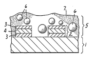
- Figure 1 is a sectional view of one embodiment of the flexible connectors of the present invention.
- FIG. 1 is a sectional view of a connector according to the invention.
- the connector is comprised of a substrate 1 with a circuit 2 comprised of a thin metallic film laminate thereon and an anisotropic electrically conductive adhesive layer 5.
- the circuit 2 consists of a thin metallic film laminate having a single copper layer 4 between two nickel layers 3.
- the anisotropic electrically conductive adhesive layer consists of an adhesive 7 with metal-covered plastic particles 6 dispersed therein.
- Metallic materials which can be used in circuits of the present invention include gold, silver, platinum, copper, palladium, chromium, nickel, tungsten, tin, lead, etc. These metallic materials are formed into films made of these metals alone or an alloy consisting of two or more of them, and laminated films made of these metals or alloys. These metallic films can be formed into circuits by evaporation, sputtering, EB method, CVD method or ion-plating method.
- three-layer laminated films comprising a layer made of nickel or an alloy containing 50% by weight or more of nickel, a layer made of copper or an alloy containing 50% by weight or more of copper and a layer made of nickel or an alloy containing 50% by weight or more of nickel are superior in conductor (surface) resistance to moisture and heating, anchor force, corrosion resistance, processability and economy.
- the thickness of circuits made of thin metallic films is preferably 1 ⁇ or less in order to maintain the bending resistance of the circuits and to prevent curling.
- the intermediate or lowermost layer may corrode.
- the thickness of the topmost nickel layer is preferably 50 Angstrom ( ⁇ ) or more.
- such laminated circuits could have the following constructions: topmost nickel layer (400 ⁇ )/intermediate copper layer (2000 ⁇ )/lowermost nickel layer (250 ⁇ ) or topmost nickel layer (100 ⁇ )/lowermost copper layer (2000 ⁇ ).
- the choice of substrates affects the cracking resistance of the laminated films made of these metals.
- the welding portion experiences localized stress.
- the effect of this stress on the metallic circuit varies largely with the modulus of elasticity of the substrate.
- the welding temperature is higher than the glass transition temperature (Tg) of PET (70° to 80°C).
- Tg glass transition temperature
- films having a high Tg e.g., 280°C or higher
- PI polyimide
- a change in the shape of the substrate by welding is so small that cracks are not readily produced. That is, particularly in the case of heat-welding, the use of substrates having a higher Tg than the vicinity of the welding temperature can markedly reduce the generation of cracks in the metallic circuit, improve the heat resistance and increase the current capacity.
- those having a Tg higher than 100°C are preferred.
- Films useful as substrates in the invention include polyimide film, polyethylene terephthalate film, polysulfone film, polyether sulfone film, polyether ketone film, polyether imide film, polyester imide film, aromatic polyamide film, polyphenylene oxide film, polyxylylene film, polyamide imide film, etc.
- the thickness of the substrate is preferably 100 ⁇ or less in order to maintain flexibility and to obtain stable connections.
- electrically conductive plastic particles may be used for the electrically conductive particle used in the anisotropic electrically conductive adhesive layer. Such particles are produced by covering the surface of spherical plastic particles with a film made of a good electrical conductor or semiconductor alone (e.g. gold, silver, copper, nickel, cobalt, palladium, chromium, aluminum, tungsten, manganese, indium, lead, tin) or an alloy consisting of these metals, or a laminated film made of these metals or alloys.
- a good electrical conductor or semiconductor alone e.g. gold, silver, copper, nickel, cobalt, palladium, chromium, aluminum, tungsten, manganese, indium, lead, tin
- an alloy consisting of these metals e.g. gold, silver, copper, nickel, cobalt, palladium, chromium, aluminum, tungsten, manganese, indium, lead, tin
- the plastic particles may be made from various plastic materials including for example particles of phenolic, epoxy, polystyrene, polyvinyl chloride, polyethylene, polypropylene, polymethacrylic ester, polyacrylic ester, polyacrylonitrile and polymethacrylonitrile series resins. Of these resin particles, particles of phenolic, epoxy and polystyrene resins are particularly preferred.
- the size of the plastic particles is preferably in a range of about 1 to 100 ⁇ and most preferably from about 3 to 50 ⁇ , as expressed by an average particle diameter.
- the thickness of the covering metal is preferably in a range of from about 50 to 5000 ⁇ in order to prevent circuit damage at the time of welding and to obtain sufficient electrical conductivity.
- Specific examples of commercially available electrically conductive particles include: Bellpearl (nickel/phenolic resin particles; produced by Kanegafuchi Spinning Co., Ltd.), MPP (nickel + gold/crosslinked polystyrene resin particles; produced by Japan Synthetic Rubber, Co., Ltd.), Toraypearl EP-M (one or more of gold, silver, copper, tin, nickel and cobalt/epoxy resin particles; produced by Toray Industries Inc.), and Micropearl (nickel/crosslinked polystyrene resin particles; produced by Sekisui Fine Chemical Co.).
- insulating adhesives such as pressure-sensitive, thermoplastic, thermosetting, photo-curing and electron ray-curing adhesives, etc.
- useful adhesives include ethylene/vinyl acetate copolymer, ethylene/propylene copolymer, ethylene/acrylic acid copolymer, ethylene/acrylic esters copolymer, acrylic esters copolymer, styrene/butadiene copolymer, styrene/isoprene copolymer, polyisobutylene rubber, silicon rubber, polyvinyl butyral resin, acrylic acid resin, cyanoacrylate resin, epoxy resin, phenol resin, phenoxy resin, polyester, polyamide and polyurethane alone or in combination.
- the content of the electrically conductive particles in the adhesive is preferably from 0.1 to 50% by volume based on the solids content of the adhesive.
- the content is less than 0.1% by volume, stable conduction is difficult to obtain, and when the content exceeds 50% by volume, it is difficult to maintain insulation between the adjacent conductors.
- the thickness of the anisotropic electrically conductive adhesive layer is dependent upon the diameter of the contained particles. It is preferably from about 0.5 to about 2 times the average particle diameter (when the particles form an aggregate, the average particle diameter means that of secondary particles).
- Metals as shown in Table 1 were each applied to several kinds of PET film and polyimide film of different thicknesses by vacuum evaporation (V) or sputtering (S), and the anchor force to the substrate, surface resistance of the thin metallic film, and corrosion resistance were measured under high-temperature and high-humidity conditions.
- V vacuum evaporation
- S sputtering
- the anchor force was evaluated as follows: Insulating tap No. 56 (produced by Sumitomo Three M Co.) was adhered to a metal surface (by one forward/backward pass of a rubber roll of 2 kg in weight) and then peeled off the surface at 180°C to measure the area of the metal surface transferred from the substrate to the tape, and the anchor force was determined by the size of the area.
- the surface resistance of the metallic film was measured using a Loresta surface resistance meter (produced by Mitsubishi Petrochemical Co., Ltd.) and is expressed by the ratio of a value after a definite period of time to the initial value.
- the corrosion resistance was evaluated as follows: Polyester resin R-251 (produced by Toray Industries Inc.) was applied in a thickness of from 10 to 20 ⁇ to each metallic film and heat-welded to slide glass. The assembly was allowed to stand in a 60°C/95% RH atmosphere and observed with the naked eye. TABLE 1 Reference Example Structure of film and thin metallic film Method of production Anchor force Surface resistance ratio of thin metallic film After 1 week /initial stage Corrosion resistance Initial stage After 1 week 1 Silver 1000 ⁇ /PET 25 ⁇ V ⁇ ⁇ 1 Stable 2 Silver 1000 ⁇ /PET 12 ⁇ (corona treatment) V .
- the substrates with a circuit comprising a thin metallic film obtained in Reference examples are an intermediate product in the course of production of the present flexible connectors; thus whether a given substrate is suitable for the present flexible connectors cannot immediately be determined from Table 1.
- the data in Table 1 indicates that the substrates of Reference examples 11 and 12 having a circuit made of a laminated metallic thin film are particularly superior in the foregoing various characteristics.
- Films with a thin metallic film composed as shown in Table 2 were prepared by evaporation on a polyimide film of 25 ⁇ in thickness, and etched using a resist to prepare a circuit pattern having conductors at an interval of 1 mm (width of conductor, 0.5 mm; gap , 0.5 mm).
- Micropearl 232 was replaced by nickel particles (average particle diameter, 32 ⁇ ; produced by Sherritt Co., Ltd.), and the measurements were carried out in the same manner as in Examples 1 to 10. These results are shown in Table 2.
- connection resistance of the flexible connectors is low over a wide range of conditions in which nickel or its alloy is used in the topmost layer of the conductor.
- Three-layer thin metallic films were prepared on a polyimide film of 25 ⁇ in thickness by applying nickel, copper and nickel to the film in that order in the thickness of 250 ⁇ , 2000 ⁇ and 400 ⁇ , respectively, by means of vacuum evaporation.
- the films were then etched using a resist to prepare a circuit pattern having conductors at an interval of 1 mm (width of conductor, 0.5 mm; gap, 0.5 mm).
- a flexible connector was prepared in the same manner as in Example 11 except that the evaporation film conductor (circuit) was of a two-layer structure of copper and nickel applied to the film in that order in the thickness of 200 ⁇ and 400 ⁇ , respectively, and that 0.6 cm3 of Micropearl 232 (produced by Sekisui Fine chemical Co.) was used as the electrically conductive plastic particles, and the properties were measured similarly. The results are shown in Table 3.
- a flexible connector was prepared in the same manner as in Example 20 except that the circuit was of a single-layer structure of nickel of 1000 ⁇ in thickness, and the properties were measured similarly. The results are shown in Table 3.
- a flexible connector was prepared in the same manner as in Example 20 except that the circuit was of a two-layer structure of nickel and copper applied to the film in this order in the thickness of 250 ⁇ and 2000 ⁇ , respectively, and the properties were measured similarly. The results are shown in Table 3.
- a flexible connector was prepared in the same manner as in Example 20 except that the circuit was of a single-layer structure of copper of 1000 ⁇ in thickness, and the properties were measured similarly. The results are shown in Table 3.
- a flexible connector was prepared in the same manner as in Example 20 except that the circuit was of a two-layer structure of copper and a nickel(7)-tin(3) alloy applied to the film in this order in the thickness of 2000 ⁇ and 400 ⁇ , respectively, and the properties were measured similarly. The results are shown in Table 3.
- a flexible connector was prepared in the same manner as in Example 20 except that the circuit was of a three-layer structure of a nickel(7)-tin(3) alloy, copper and a nickel(7)-tin(3) alloy which were applied to the film in this order in the thickness of 250 ⁇ , 2000 ⁇ and 400 ⁇ , respectively. The properties were measured similarly. The results are shown in Table 3.
- the data indicate that with connectors according to the present invention, cracks do not form in the circuit at the time of application.
- the data further indicate that the present invention provides connectors that can maintain stable and low connection resistance over a long period of time even under humid and heated circumstances, that have excellent conduction characteristics and that are rich in flexibility.
Landscapes
- Engineering & Computer Science (AREA)
- Microelectronics & Electronic Packaging (AREA)
- Manufacturing & Machinery (AREA)
- Physics & Mathematics (AREA)
- Thermal Sciences (AREA)
- Adhesive Tapes (AREA)
- Laminated Bodies (AREA)
- Devices For Indicating Variable Information By Combining Individual Elements (AREA)
- Adhesives Or Adhesive Processes (AREA)
- Non-Insulated Conductors (AREA)
Applications Claiming Priority (2)
| Application Number | Priority Date | Filing Date | Title |
|---|---|---|---|
| JP199678/87 | 1987-08-10 | ||
| JP62199678A JPS6445074A (en) | 1987-08-10 | 1987-08-10 | Flexible connector |
Publications (2)
| Publication Number | Publication Date |
|---|---|
| EP0303384A2 true EP0303384A2 (de) | 1989-02-15 |
| EP0303384A3 EP0303384A3 (de) | 1989-10-25 |
Family
ID=16411794
Family Applications (1)
| Application Number | Title | Priority Date | Filing Date |
|---|---|---|---|
| EP88307130A Withdrawn EP0303384A3 (de) | 1987-08-10 | 1988-08-02 | Biegsames Verbindungsband |
Country Status (4)
| Country | Link |
|---|---|
| EP (1) | EP0303384A3 (de) |
| JP (1) | JPS6445074A (de) |
| KR (1) | KR890004599A (de) |
| MY (1) | MY103340A (de) |
Cited By (3)
| Publication number | Priority date | Publication date | Assignee | Title |
|---|---|---|---|---|
| EP0530780A1 (de) * | 1991-09-03 | 1993-03-10 | Nitto Denko Corporation | Folie oder Band zum Herstellen von elektrischen Verbindungen und Verfahren zum Herstellen einer solchen Verbindung |
| US7773337B2 (en) * | 2006-02-10 | 2010-08-10 | Seagate Technology Llc | Tamper evident tape with integrated EMI shielding |
| US8000491B2 (en) | 2006-10-24 | 2011-08-16 | Nokia Corporation | Transducer device and assembly |
Family Cites Families (5)
| Publication number | Priority date | Publication date | Assignee | Title |
|---|---|---|---|---|
| EP0134624A3 (de) * | 1983-06-13 | 1987-05-13 | Minnesota Mining And Manufacturing Company | Klebebandmehrfachverbindung |
| JPS60140685A (ja) * | 1983-12-28 | 1985-07-25 | 日本写真印刷株式会社 | フイルム状電極コネクタ及びその製造方法 |
| JPS61173471A (ja) * | 1985-01-28 | 1986-08-05 | シャープ株式会社 | 熱圧着コネクタ− |
| JPS61195569A (ja) * | 1985-02-25 | 1986-08-29 | 松下電器産業株式会社 | フイルムコネクタ及びその製造方法 |
| US4740657A (en) * | 1986-02-14 | 1988-04-26 | Hitachi, Chemical Company, Ltd | Anisotropic-electroconductive adhesive composition, method for connecting circuits using the same, and connected circuit structure thus obtained |
-
1987
- 1987-08-10 JP JP62199678A patent/JPS6445074A/ja active Pending
-
1988
- 1988-08-02 EP EP88307130A patent/EP0303384A3/de not_active Withdrawn
- 1988-08-05 MY MYPI88000893A patent/MY103340A/en unknown
- 1988-08-09 KR KR1019880010157A patent/KR890004599A/ko not_active Withdrawn
Cited By (5)
| Publication number | Priority date | Publication date | Assignee | Title |
|---|---|---|---|---|
| EP0530780A1 (de) * | 1991-09-03 | 1993-03-10 | Nitto Denko Corporation | Folie oder Band zum Herstellen von elektrischen Verbindungen und Verfahren zum Herstellen einer solchen Verbindung |
| US5342468A (en) * | 1991-09-03 | 1994-08-30 | Nitto Denko Corporation | Joint forming sheet or tape and method for joint formation using the same |
| US7773337B2 (en) * | 2006-02-10 | 2010-08-10 | Seagate Technology Llc | Tamper evident tape with integrated EMI shielding |
| US7911733B2 (en) | 2006-02-10 | 2011-03-22 | Seagate Technology Llc | Tamper evident tape with integrated EMI shielding |
| US8000491B2 (en) | 2006-10-24 | 2011-08-16 | Nokia Corporation | Transducer device and assembly |
Also Published As
| Publication number | Publication date |
|---|---|
| KR890004599A (ko) | 1989-04-22 |
| MY103340A (en) | 1993-05-29 |
| JPS6445074A (en) | 1989-02-17 |
| EP0303384A3 (de) | 1989-10-25 |
Similar Documents
| Publication | Publication Date | Title |
|---|---|---|
| US4642421A (en) | Adhesive electrical interconnecting means | |
| JP3530980B2 (ja) | 接着構造、液晶装置、及び電子機器 | |
| US20050211464A1 (en) | Method of microelectrode connection and connected structure of use threof | |
| WO1986006551A1 (en) | Flexible electrical jumper cable and assembly | |
| US4931598A (en) | Electrical connector tape | |
| JP2000195339A (ja) | 異方導電性接着フィルム | |
| EP4163347A1 (de) | Verfahren zur herstellung eines gebundenen körpers, gebundener körper und heissschmelzklebefolie mit elektrisch leitfähigen partikeln | |
| JPH0253911B2 (de) | ||
| KR101163436B1 (ko) | 절연 피복 도전 입자 | |
| JPH07157720A (ja) | 異方導電フィルム | |
| EP0501270A1 (de) | Elektronische Vorrichtung mit uniaxial leitfähiger Klebezusammensetzung | |
| JP3622792B2 (ja) | 接続部材及び該接続部材を用いた電極の接続構造・接続方法 | |
| EP0303384A2 (de) | Biegsames Verbindungsband | |
| JPH06103819A (ja) | 異方導電性接着フィルム | |
| GB2222327A (en) | Hot-melt adhesive anisotropic interconnector | |
| KR100961589B1 (ko) | 접착재 릴 및 이를 이용한 회로 접속체의 제조 방법 | |
| JPS61195179A (ja) | 異方導電性接着シ−ト | |
| JPS63231889A (ja) | 回路の接続部材 | |
| JPH08249922A (ja) | 被覆粒子 | |
| KR100406090B1 (ko) | 이방성 도전 필름 | |
| JP3944794B2 (ja) | 回路の接続構造 | |
| JP5082296B2 (ja) | 配線付き接着剤及び回路接続構造 | |
| JP4155470B2 (ja) | 接続部材を用いた電極の接続法 | |
| JPS63227687A (ja) | 導電性両面接着テ−プ | |
| JPS6215777A (ja) | フイルム状コネクタ及びその製造方法 |
Legal Events
| Date | Code | Title | Description |
|---|---|---|---|
| PUAI | Public reference made under article 153(3) epc to a published international application that has entered the european phase |
Free format text: ORIGINAL CODE: 0009012 |
|
| AK | Designated contracting states |
Kind code of ref document: A2 Designated state(s): DE FR GB IT |
|
| PUAL | Search report despatched |
Free format text: ORIGINAL CODE: 0009013 |
|
| AK | Designated contracting states |
Kind code of ref document: A3 Designated state(s): DE FR GB IT |
|
| 17P | Request for examination filed |
Effective date: 19900418 |
|
| 17Q | First examination report despatched |
Effective date: 19920428 |
|
| STAA | Information on the status of an ep patent application or granted ep patent |
Free format text: STATUS: THE APPLICATION IS DEEMED TO BE WITHDRAWN |
|
| 18D | Application deemed to be withdrawn |
Effective date: 19921110 |