EP0303216A2 - Dielektrisches Filter und dessen Herstellungsverfahren - Google Patents
Dielektrisches Filter und dessen Herstellungsverfahren Download PDFInfo
- Publication number
- EP0303216A2 EP0303216A2 EP88112879A EP88112879A EP0303216A2 EP 0303216 A2 EP0303216 A2 EP 0303216A2 EP 88112879 A EP88112879 A EP 88112879A EP 88112879 A EP88112879 A EP 88112879A EP 0303216 A2 EP0303216 A2 EP 0303216A2
- Authority
- EP
- European Patent Office
- Prior art keywords
- edge portion
- layer
- dielectric filter
- top surface
- conductive layer
- Prior art date
- Legal status (The legal status is an assumption and is not a legal conclusion. Google has not performed a legal analysis and makes no representation as to the accuracy of the status listed.)
- Granted
Links
- 238000004519 manufacturing process Methods 0.000 title claims abstract description 5
- 239000004020 conductor Substances 0.000 claims abstract description 20
- 238000000034 method Methods 0.000 claims abstract description 7
- 230000004044 response Effects 0.000 claims description 6
- 229910010293 ceramic material Inorganic materials 0.000 abstract description 6
- 230000009467 reduction Effects 0.000 abstract description 6
- 238000009966 trimming Methods 0.000 description 5
- 230000008569 process Effects 0.000 description 3
- RYGMFSIKBFXOCR-UHFFFAOYSA-N Copper Chemical compound [Cu] RYGMFSIKBFXOCR-UHFFFAOYSA-N 0.000 description 2
- GWEVSGVZZGPLCZ-UHFFFAOYSA-N Titan oxide Chemical compound O=[Ti]=O GWEVSGVZZGPLCZ-UHFFFAOYSA-N 0.000 description 2
- 230000008901 benefit Effects 0.000 description 2
- 229910052802 copper Inorganic materials 0.000 description 2
- 239000010949 copper Substances 0.000 description 2
- 239000003989 dielectric material Substances 0.000 description 2
- 239000000463 material Substances 0.000 description 2
- 229910052709 silver Inorganic materials 0.000 description 2
- 239000004332 silver Substances 0.000 description 2
- 230000006978 adaptation Effects 0.000 description 1
- 230000008878 coupling Effects 0.000 description 1
- 238000010168 coupling process Methods 0.000 description 1
- 238000005859 coupling reaction Methods 0.000 description 1
- 230000003247 decreasing effect Effects 0.000 description 1
- 238000012986 modification Methods 0.000 description 1
- 230000004048 modification Effects 0.000 description 1
Images

Classifications
-
- H—ELECTRICITY
- H01—ELECTRIC ELEMENTS
- H01P—WAVEGUIDES; RESONATORS, LINES, OR OTHER DEVICES OF THE WAVEGUIDE TYPE
- H01P1/00—Auxiliary devices
- H01P1/20—Frequency-selective devices, e.g. filters
- H01P1/201—Filters for transverse electromagnetic waves
- H01P1/202—Coaxial filters
-
- H—ELECTRICITY
- H01—ELECTRIC ELEMENTS
- H01P—WAVEGUIDES; RESONATORS, LINES, OR OTHER DEVICES OF THE WAVEGUIDE TYPE
- H01P1/00—Auxiliary devices
- H01P1/20—Frequency-selective devices, e.g. filters
- H01P1/201—Filters for transverse electromagnetic waves
- H01P1/205—Comb or interdigital filters; Cascaded coaxial cavities
- H01P1/2056—Comb filters or interdigital filters with metallised resonator holes in a dielectric block
Definitions
- the present invention relates to a dielectric filter comprised of ceramic material, and more particularly to a dielectric filter and its method of manufacturing,to which radio frequency signals (hereinafter referred to as RF signals) having a frequency from the ultra high frequency (UHF) bands to the relatively low frequency microwave bands can be coupled, and which is well adapted for a bandpass filter coupling to RF signals having either of the frequency ranges from 825 MHz to 845 MHz or from 870 MHz to 890 MHz, which are used by mobile telephones.
- RF signals radio frequency signals having a frequency from the ultra high frequency (UHF) bands to the relatively low frequency microwave bands
- UHF ultra high frequency
- a dielectric filter must be tuned after the filter is initially constructed and tested.
- a conventional dielectric filter structure whose frequency response may be finely adjusted is described in detail in U.S. Patent No. 4,431,977 and Japanese laid-open Patent Publication No. 84-128801.
- a fine frequency adjustment of the filter described in U.S. Patent No. 4,431,977 is performed by removing an amount of the conductive material from around the conductor-lined holes formed in the dielectric material, the amount of the material removed determining the amount of adjustment.
- the dielectic filter of the present invention includes a block of ceramic material having one or more holes extending from a top surface to a bottom surface, each of which is interiorly covered with conductive material so as to form an inner conductive layer.
- the bottom surface and side surfaces of the block are similarly covered with bottom and side conductive layers electrically connected to the inner conductive layers at the bottom surface.
- the inner conductive layer is further connected to spaced apart top conductive layer portions provided on the top surface of the block surrounding each hole.
- the top layer portions are spaced from each other and have an oblique edge portion which is capacitively coupled with, and obliquely faces an upper edge portion of the side conductive layers.
- the filter is designed to initially have a resonant frequency which is greater than that ultimately desired, and after measuring the resonant frequency initially obtained, a portion of the top conductive layer is removed in order to reduce the resonant frequency to a desired value.
- the amount by which the resonant frequency is reduced by removing a portion of the top conductive layer depends not only on the amount of material removed, but also on the distance from the removed portion to the opposing upper edge portion of the side layer. Therefore, the resonant frequency of the filter can be, and in accordance with the method of the invention is, reduced by a predetermined amount by selection of a location along the oblique edge portion appropriate to the amount of reduction required for removal of a predetermined amount of conductive material.
- the oblique edge portion of the top conductive layer is straight or uniformly staircase-shaped and the upper edge portion of the side layer is straight, so that the distance between them changes in a linear or uniformly incremental manner. This facilitates the selection of the appropriate location for the removal of conductive material depending on the amount by which the resonant frequency must be reduced.
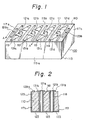
- a dielectric filter 100 embodying the present invention.
- Each of the interior surfaces in the block 110 is entirely covered with a layer of a conductive material such as a silver or copper so as to form inner conductive layers 121a, 121b, 121c and 121d as shown in Fig. 2, which is a cross section of the dielectric filter 100 in Fig. 1 taken along lines A-A.
- a conductive material such as a silver or copper
- the inner conductive layers 121a-121d are electrically connected with one another by means of a bottom conductive layer 123 which may also be formed, for example, of silver or copper on the bottom surface 113 of the block 110.
- the bottom conductive layer 123 is electrically connected with similarly formed side conductive layers 125 provided on the side surfaces 115a, 115b, 117a, and 117b.
- the four resonators have respective top conductive layers 131 on the top surface 111, designated layers or layer portions 131a, 131b, 131c and 131d.
- the top conductive layers 131a-131d respectively form collars covering the portions of the top surface 111 surrounding the four corresponding holes 119 and are respectively connected to the corresponding inner conductive layers 121a-121d.
- each of the conductive layers 121, 123, 125 and 131 is about 2 microns.
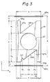
- FIG. 3 there is illustrated a partial plan view of the filter 100 shown in Fig. 1.
- the exemplary top layer 131 as shown in Fig. 3 has a rectangular configuration, and has side edge portions 126a and 126b respectively facing the straight upper edge portions 125a and 125b of the side conductive layer 125.
- the side edge portions 126a and 126b are respectively provided with substantial identical right angled triangle shaped recesses 127a and 127b.
- the width (a) of the filter 100 is 6.00mm; the width (b) of each top layer 131 is 3.00mm; each of the distances (c1) and (c2) between the side portions 126a, 126b and the upper edge portions 125a, 125b is 0.5mm; the length (d) of the top layer 131 is 5.00mm; the depths (e1) and (e2) of the recesses 127a and 127b are each 1.50mm; the diameter (f) of the inner conductive layer 121 is 2.00mm; the lengths (g1) and (g2) of the sections of each of the conductive layer edge portions 126a and 126b which are parallel to the upper edge portions 125a and 125b is 0.50mm; and the base (h) of each of recesses 127a and 127b is 2.00mm.
- the frequency response of a resonator having the above-mentioned structure can be adjusted by changing its capacitance which is mainly established between the upper edge portions 125a and 125b and the side edge portions 126a and 126b including the straight oblique edge portions 128a and 128b formed by the recesses 127a and 127b.
- the capacitance can be reduced by removing in the form of a notch 130 a portion of the conductive from the top conductive layer 131 by means of a sandblast trimmer or a laser trimmer.
- the amount of reduction in the capacitance is deter necessarilymined by the location or locations of one or more such notches 130 along the oblique edge portions 128a and 128b, defined, for example, by its X-coordinate as measured along the upper edge portions I25a and 125b as shown in Fig. 3.
- the resonant frequency of the resonator is sharply reduced because the oblique edge portion 128b at X1 is relatively close to the upper edge portion 125b and, therefore, sets up a relatively large capacitance with the upper edge portion 125b.
- the resonant frequency of the resonator is only slightly reduced because the oblique edge portion at X3 is relatively far from the upper edge portion 125b and, therefore, creates a relatively small capacitance with the upper edge portion.
- the resonant frequency of the resonator experiences an intermediate reduction.
- the resonant frequency of the resonator therefore, can be adjusted within a large range of values by choosing a trimming location on an oblique edge portion and forming there a notch of a dimension previously selected independently of the location.
- the X-coordinates X1 and X2 are respectively distances i1 and i2 from the center location X2 equal to 0.75mm and distances j1 and j2 from the respective extremes of the oblique edge portion 128b equal to 0.25mm.
- the resonant frequency of the resonator in Fig. 3, of which the center frequency is around 880MHz, is reduced by 2.0MHz in the case of removing 1.57mm2 of the conductive material from the oblique edge portion 128b at the X-coordinate X1 and is reduced by 0.2MHz in the case of removing 1.57mm2 of the conductive material from the oblique edge portion 128b at the X-coordinate X3.
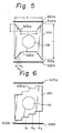
- the conductive layer 531 in Fig. 5 has a rectangular configuration, of which the length (a) is 5.00mm, the width (b) is 4.0mm, and side edge portions 532a and 532b, facing each of upper edge portions 525a and 525b, are provided with respective regular trapezoid shaped recesses 526a and 526b.
- Each of the trapezoid shaped recesses has a short side (c) 2.40mm long and a height (d) of 1.00mm, and also has two staircase-shaped oblique sides, respectively consisting of four steps, each of the treads of which is 0.20mm long and each of the risers of which is 0.25mm high.
- the other dimensions of the resonator in Fig. 5 are substantially the same as those of the resonator shown in Fig. 3.
- the staircase-shaped oblique sides facilitate automation of the trimming process by reducing the need for precision in locating the X-coordinates where the notch is to be placed.
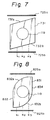
- FIG. 6 there is illustrated a third embodiment according to the present invention.
- the top conductive layer 631 in Fig. 6 has staircase-shaped edge portions 632a and 632b respectively facing upper edge portions 625a and 625b, each of four steps thereof defining a right-angle triangle-shaped recess.
- the tread of each of the steps is 1.0mm long and the riser of each step is 0.40mm high.
- the other dimensions of the resonator shown in Fig. 6 are substantially the same as those of the resonator shown in Fig. 5.
- This embodiment has a similar advantage to that of Fig. 5 in reducing the need for precision in locating where the notch is to be placed, particularly in an automated trimming process.
- FIGs. 7 and 8 there are illustrated two other embodiments according to the present invention.
- the conductive layers 731 in Fig. 7 has a parallelogram configuration, having a pair of edge portions 732a and 732b obliquely facing respective side conductive layer upper edge portions 725a and 725b.
- the conductive layer 831 in Fig. 8 has a configuration in which edge portions 832a and 832b, respectively obliquely facing conductive side layer upper edge portions 825a and 825b, curve away from the latter edge portions from left to right and from right to left, respectively.
- locations along oblique edge portions have varying predetermined distances from the outer conductive layer edge portion.
- the resonant frequency of the resonator can be reduced from a relatively large amount to a relatively small amount by removing a predetermined same amount of the conductive material from an appropriately selected location along the oblique edge portion.
- the top surface of the filter is covered with a regular pattern of the conductive layers surrounding the holes to form with the upper edge portions 125a and 125b a plurality of resonators. Since there are no exposed portions of ceramic material on the top surface between the inner conductive layer and the top conductive layer, little reduction of the unloaded Qu of the filter will occur.
- the present disclosure relates to the subject matter disclosed in Japanese Application 62-198873 of August 8th, 1987, the entire disclosure of which is incorporated herein by reference.
Landscapes
- Physics & Mathematics (AREA)
- Electromagnetism (AREA)
- Control Of Motors That Do Not Use Commutators (AREA)
Applications Claiming Priority (2)
| Application Number | Priority Date | Filing Date | Title |
|---|---|---|---|
| JP198873/87 | 1987-08-08 | ||
| JP62198873A JPH0612841B2 (ja) | 1987-08-08 | 1987-08-08 | 誘電体フィルタの周波数調整方法 |
Publications (3)
| Publication Number | Publication Date |
|---|---|
| EP0303216A2 true EP0303216A2 (de) | 1989-02-15 |
| EP0303216A3 EP0303216A3 (en) | 1990-05-16 |
| EP0303216B1 EP0303216B1 (de) | 1993-12-08 |
Family
ID=16398339
Family Applications (1)
| Application Number | Title | Priority Date | Filing Date |
|---|---|---|---|
| EP88112879A Expired - Lifetime EP0303216B1 (de) | 1987-08-08 | 1988-08-08 | Dielektrisches Filter und dessen Herstellungsverfahren |
Country Status (6)
| Country | Link |
|---|---|
| US (1) | US4855693A (de) |
| EP (1) | EP0303216B1 (de) |
| JP (1) | JPH0612841B2 (de) |
| KR (1) | KR920002029B1 (de) |
| CA (1) | CA1287131C (de) |
| DE (1) | DE3886128T2 (de) |
Cited By (3)
| Publication number | Priority date | Publication date | Assignee | Title |
|---|---|---|---|---|
| WO2008133932A1 (en) * | 2007-04-27 | 2008-11-06 | Cts Corporation | Coaxial resonator |
| CN112072240A (zh) * | 2020-08-28 | 2020-12-11 | 潮州三环(集团)股份有限公司 | 一种介质波导滤波器及其制作方法 |
| CN112164855A (zh) * | 2020-08-28 | 2021-01-01 | 深圳顺络电子股份有限公司 | 一种介质滤波器自动调试方法及系统 |
Families Citing this family (11)
| Publication number | Priority date | Publication date | Assignee | Title |
|---|---|---|---|---|
| JPH07105644B2 (ja) * | 1988-10-18 | 1995-11-13 | 沖電気工業株式会社 | 有極型誘電体フィルタ |
| US5004992A (en) * | 1990-05-25 | 1991-04-02 | Motorola, Inc. | Multi-resonator ceramic filter and method for tuning and adjusting the resonators thereof |
| DE69118774T2 (de) * | 1990-08-08 | 1996-11-28 | Oki Electric Ind Co Ltd | Ultraschallschleifsystem für keramisches Filter und Verfahren zum Abgleich dafür |
| US6081174A (en) | 1997-03-14 | 2000-06-27 | Taiyo Yuden Co., Ltd. | Wave filter having two or more coaxial dielectric resonators in juxtaposition |
| US6147572A (en) * | 1998-07-15 | 2000-11-14 | Lucent Technologies, Inc. | Filter including a microstrip antenna and a frequency selective surface |
| US6650202B2 (en) * | 2001-11-03 | 2003-11-18 | Cts Corporation | Ceramic RF filter having improved third harmonic response |
| US20050219013A1 (en) * | 2004-04-06 | 2005-10-06 | Pavan Kumar | Comb-line filter |
| US7541893B2 (en) * | 2005-05-23 | 2009-06-02 | Cts Corporation | Ceramic RF filter and duplexer having improved third harmonic response |
| CN104009276A (zh) | 2013-02-25 | 2014-08-27 | 中兴通讯股份有限公司 | 介质谐振器及其装配方法、介质滤波器 |
| CN104037484A (zh) * | 2013-03-08 | 2014-09-10 | 中兴通讯股份有限公司 | 介质谐振器及介质滤波器 |
| CN111313136B (zh) * | 2019-12-13 | 2021-08-17 | 新益技术(深圳)有限公司 | 一种介质滤波器自动调试系统以及方法 |
Family Cites Families (7)
| Publication number | Priority date | Publication date | Assignee | Title |
|---|---|---|---|---|
| JPS5574223A (en) * | 1978-11-30 | 1980-06-04 | Tdk Corp | Trimming unit |
| US4431977A (en) * | 1982-02-16 | 1984-02-14 | Motorola, Inc. | Ceramic bandpass filter |
| JPS58179002A (ja) * | 1982-04-15 | 1983-10-20 | Oki Electric Ind Co Ltd | 誘電体フイルタ |
| GB2165098B (en) * | 1984-09-27 | 1988-05-25 | Motorola Inc | Radio frequency filters |
| US4742562A (en) * | 1984-09-27 | 1988-05-03 | Motorola, Inc. | Single-block dual-passband ceramic filter useable with a transceiver |
| US4768003A (en) * | 1984-09-28 | 1988-08-30 | Oki Electric Industry Co., Inc. | Microwave filter |
| DE3506471A1 (de) * | 1985-02-23 | 1986-08-28 | Brown, Boveri & Cie Ag, 6800 Mannheim | Verfahren zur abstimmung eines dielektrischen resonators |
-
1987
- 1987-08-08 JP JP62198873A patent/JPH0612841B2/ja not_active Expired - Lifetime
-
1988
- 1988-08-03 US US07/227,874 patent/US4855693A/en not_active Expired - Lifetime
- 1988-08-05 CA CA000573943A patent/CA1287131C/en not_active Expired - Fee Related
- 1988-08-08 EP EP88112879A patent/EP0303216B1/de not_active Expired - Lifetime
- 1988-08-08 KR KR1019880010120A patent/KR920002029B1/ko not_active Expired
- 1988-08-08 DE DE3886128T patent/DE3886128T2/de not_active Expired - Fee Related
Cited By (4)
| Publication number | Priority date | Publication date | Assignee | Title |
|---|---|---|---|---|
| WO2008133932A1 (en) * | 2007-04-27 | 2008-11-06 | Cts Corporation | Coaxial resonator |
| US7830229B2 (en) | 2007-04-27 | 2010-11-09 | Cts Corporation | Coaxial resonator including a metallized area with interdigitated fingers |
| CN112072240A (zh) * | 2020-08-28 | 2020-12-11 | 潮州三环(集团)股份有限公司 | 一种介质波导滤波器及其制作方法 |
| CN112164855A (zh) * | 2020-08-28 | 2021-01-01 | 深圳顺络电子股份有限公司 | 一种介质滤波器自动调试方法及系统 |
Also Published As
| Publication number | Publication date |
|---|---|
| DE3886128T2 (de) | 1994-07-07 |
| JPH0612841B2 (ja) | 1994-02-16 |
| JPS6442901A (en) | 1989-02-15 |
| KR890004465A (ko) | 1989-04-22 |
| CA1287131C (en) | 1991-07-30 |
| KR920002029B1 (ko) | 1992-03-09 |
| EP0303216B1 (de) | 1993-12-08 |
| EP0303216A3 (en) | 1990-05-16 |
| DE3886128D1 (de) | 1994-01-20 |
| US4855693A (en) | 1989-08-08 |
Similar Documents
| Publication | Publication Date | Title |
|---|---|---|
| EP0303216A2 (de) | Dielektrisches Filter und dessen Herstellungsverfahren | |
| US6400238B1 (en) | Dielectric filter having side surface indentation | |
| FI78797B (fi) | Keramiskt bandpassfilter. | |
| KR101740292B1 (ko) | 대역폭 조정을 위한 방법 및 구조물을 갖는 유전체 도파관 필터 | |
| EP3319166A1 (de) | Dielektrisches filter, sende-empfänger und basisstation | |
| US9030278B2 (en) | Tuned dielectric waveguide filter and method of tuning the same | |
| US4890079A (en) | Di-electric bandpass filter | |
| US6275125B1 (en) | Wave filter having two or more coaxial dielectric resonators in juxtaposition | |
| EP0415558B1 (de) | Bandpassfilter und Verfahren zum Abgleichen von dessen Charakteristika | |
| JPH0369202B2 (de) | ||
| US4839618A (en) | Monolithic crystal filter with wide bandwidth and method of making same | |
| KR102439016B1 (ko) | 캐비티 필터 및 이의 제조방법 | |
| EP3451440A1 (de) | Hochfrequenzfilter | |
| US6005456A (en) | Dielectric filter having non-conductive adjusting regions | |
| KR100268527B1 (ko) | 유전체필터및그의제조방법 | |
| KR19990023340A (ko) | 유전체 필터 및 그 제조방법 | |
| JPH0563411A (ja) | 同軸型誘電体共振器 | |
| JP3322334B2 (ja) | 誘電体ブロック型フィルタ | |
| EP1009059A1 (de) | Dielektrisches Filter mit regelbarer Frequenzbandbreite | |
| JPH08321702A (ja) | 誘電体フィルタ及びその周波数帯域幅の調整方法 | |
| US6522224B2 (en) | Method for adjusting characteristics of a dielectric filter | |
| US5896074A (en) | Dielectric filter | |
| JPH07131212A (ja) | 誘電体共振器の共振周波数の調整方法 | |
| JPH1056308A (ja) | 誘電体フィルタの製造方法 | |
| JPH05175702A (ja) | 一体型誘電体フィルタ |
Legal Events
| Date | Code | Title | Description |
|---|---|---|---|
| PUAI | Public reference made under article 153(3) epc to a published international application that has entered the european phase |
Free format text: ORIGINAL CODE: 0009012 |
|
| AK | Designated contracting states |
Kind code of ref document: A2 Designated state(s): DE FR GB |
|
| PUAL | Search report despatched |
Free format text: ORIGINAL CODE: 0009013 |
|
| AK | Designated contracting states |
Kind code of ref document: A3 Designated state(s): DE FR GB |
|
| 17P | Request for examination filed |
Effective date: 19900620 |
|
| 17Q | First examination report despatched |
Effective date: 19920724 |
|
| GRAA | (expected) grant |
Free format text: ORIGINAL CODE: 0009210 |
|
| AK | Designated contracting states |
Kind code of ref document: B1 Designated state(s): DE FR GB |
|
| REF | Corresponds to: |
Ref document number: 3886128 Country of ref document: DE Date of ref document: 19940120 |
|
| ET | Fr: translation filed | ||
| PLBE | No opposition filed within time limit |
Free format text: ORIGINAL CODE: 0009261 |
|
| STAA | Information on the status of an ep patent application or granted ep patent |
Free format text: STATUS: NO OPPOSITION FILED WITHIN TIME LIMIT |
|
| 26N | No opposition filed | ||
| PGFP | Annual fee paid to national office [announced via postgrant information from national office to epo] |
Ref country code: GB Payment date: 19980731 Year of fee payment: 11 |
|
| PGFP | Annual fee paid to national office [announced via postgrant information from national office to epo] |
Ref country code: FR Payment date: 19980814 Year of fee payment: 11 |
|
| PGFP | Annual fee paid to national office [announced via postgrant information from national office to epo] |
Ref country code: DE Payment date: 19980817 Year of fee payment: 11 |
|
| PG25 | Lapsed in a contracting state [announced via postgrant information from national office to epo] |
Ref country code: GB Free format text: LAPSE BECAUSE OF NON-PAYMENT OF DUE FEES Effective date: 19990808 |
|
| GBPC | Gb: european patent ceased through non-payment of renewal fee |
Effective date: 19990808 |
|
| PG25 | Lapsed in a contracting state [announced via postgrant information from national office to epo] |
Ref country code: FR Free format text: LAPSE BECAUSE OF NON-PAYMENT OF DUE FEES Effective date: 20000428 |
|
| PG25 | Lapsed in a contracting state [announced via postgrant information from national office to epo] |
Ref country code: DE Free format text: LAPSE BECAUSE OF NON-PAYMENT OF DUE FEES Effective date: 20000601 |
|
| REG | Reference to a national code |
Ref country code: FR Ref legal event code: ST |