EP0302779A2 - Nichtflüchtige latente Speicherzelle mit Pegelumformerschaltung und reduzierter Tunneleffektschaltung für verbesserte Betriebssicherheit - Google Patents
Nichtflüchtige latente Speicherzelle mit Pegelumformerschaltung und reduzierter Tunneleffektschaltung für verbesserte Betriebssicherheit Download PDFInfo
- Publication number
- EP0302779A2 EP0302779A2 EP88401990A EP88401990A EP0302779A2 EP 0302779 A2 EP0302779 A2 EP 0302779A2 EP 88401990 A EP88401990 A EP 88401990A EP 88401990 A EP88401990 A EP 88401990A EP 0302779 A2 EP0302779 A2 EP 0302779A2
- Authority
- EP
- European Patent Office
- Prior art keywords
- circuit
- volatile
- node
- drive transistor
- level shifting
- Prior art date
- Legal status (The legal status is an assumption and is not a legal conclusion. Google has not performed a legal analysis and makes no representation as to the accuracy of the status listed.)
- Granted
Links
Images


Classifications
-
- G—PHYSICS
- G11—INFORMATION STORAGE
- G11C—STATIC STORES
- G11C14/00—Digital stores characterised by arrangements of cells having volatile and non-volatile storage properties for back-up when the power is down
Definitions
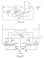
- the invention relates to a non-volatile CMOS or NMOS shadow storage cell in which the number of isolation tunnel devices and the associated required silicon area is reduced by fifty percent and wherein improved level shifter(s) may be utilized in the input/output portion of the circuit.
- Non-volatile memory cells are commonly used to store data derived from an associated volatile memory cell so that the data is not lost during a power-off period. These non-volatile cells are commonly referred to as "shadow" cells.
- the connections between the non-volatile cell and the volatile cell are usually bi-directional; they function as inputs during a non-volatile store operation and as outputs during a recall of the data to the volatile cell from the non-volatile cell.
- a source of relatively high voltage on the order of from 10 to 20 volts, induces tunneling in one of a pair of Fowler-Nordheim (FN) isolation elements in the non-volatile cell during store operations.
- the FN element has a very high impedance when not in a tunneling state so that the stored charge is isolated from the rest of the circuit during power-off.
- the FN element may be considered as a bi-directional voltage triggered switch, similar to a pair of Zener diodes connected back to back. If the absolute potential across the FN element is less than the Fowler-Nordheim voltage the element is non-conducting and if the potential exceeds the Fowler-Nordheim voltage, then the element conducts with a very low impedance.
- the advantage of the cell of Figure 1 lies in the fact that it may be easily connected to a volatile storage element (not shown) via nodes D, D and that such connection does not interfere with normal operation of the volatile element. Thus, it is possible and practical to achieve both high speed operation and non-volatility.
- Recall of the non-volatile data occurs via node 21 which is usually connected to the volatile memory cell which provided the D and D inputs.
- With single controlling transistor Q24 and floating node 32 it is necessary to provide a minimum voltage difference between the two complementary data states of at least two to three volts because sensing transistor Q24 must be turned on strongly enough in one data state to overcome the volatile element should it be in the opposite state.
- the voltage difference between the two complementary data states of the non-volatile element is directly related to the amount of charge passed through FN tunneling elements 20, 22.
- tunneling elements 20, 22 are, in turn, directly related to the oxide charge transfer and it is desirable to minimize the tunneling charge transfer to achieve maximum reliability.
- reliability is significantly dependent upon the oxide electric field/current density and therefore, another objective is to minimize oxide current density.
- FN devices 20, 22 always form a series path between the high voltage source and ground. This means that the high voltage must be chosen so that it never exceeds twice the Fowler-Nordheim voltage of the tunneling elements since, under that condition, both devices would conduct and a large current would flow from the high voltage node to the ground node. Such a large current would impact the reliability of the FN devices severely. It is clear that if either FN device of the pair were to fail, the circuit would disfunction.
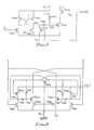
- the invention utilizes an improved level shifting circuit and method for performing the level shifting function as required in the design of non-volatile shadow memory cells.
- the improved circuit may be implemented in either P-well CMOS or N-well CMOS; in either case the advantages over the prior art are recognized. Furthermore, because there is no capacitive gate boosting utilized, the circuit is static; i.e.; it is d.c. coupled and the required silicon area is much reduced over that of the prior art circuits.
- the level shifter employs a latching circuit driven by a pair of input transistors whose drains are coupled to the gates of the latch circuit. The input(s) to the circuit are connected to the gates of the two input transistors.
- a single FN device is used to both charge and discharge the non-volatile storage device reducing the "walkout" effect in the FN device and improving its reliability.
- an object of the invention to provide an improved static level shifting circuit for a non-volatile memory cell wherein the gate of a drive transistor is not capacitively boosted and significant reduction of required silicon area is the result.
- circuit of Figure 3 illustrates the substitution of an improved level shifting clrcuit 41 for circuit 40 of Figure 1.
- Circuit 41 is a level shifter including FET Q44 with its gate connected to input terminal D .
- the sink electrode of Q44 is connected to ground.
- the drain electrode of Q44 is connected to the sink electrode of P-channel FET Q46 and to the gate electrode of P-channel FET Q50.
- the drain electrode of Q46 and the drain electrode of Q50 are connected to HV, the high voltage source.
- the gate of Q46 is connected to the drain electrode of FET Q48, the drain electrode of Q52 and to the sink electrode of P-channel FET Q50 (the common connection is node 54). Node 54 is connected to the left side of C26.
- the gate of Q48 is connected to input terminal D.
- the sink electrode of Q48 is connected to ground.
- the gate electrode of Q52 is connected to RECALL terminal 60.
- the sink electrode of Q52 is connected to ground.
- Transistors Q46 and Q50 comprise a latching circuit with feedback provided from the sink of each to the gate of the other.
- Node 32 is, of course, connected to the floating gate of controlling transistor Q24.
- Circuit 41 acts to switch the programming voltage, HV, as needed within the non-volatile storage cell of the improved circuit shown in Figure 3. If the state of the volatile storage element (connected to D and D , but not shown) is such that terminal D is at a high level and terminal D is at a low level, then node 54 is held low by N-channel FET Q48. P-channel FET Q46 (with a low level on its gate) then connects the gate of FET Q50 to HV and Q50 is turned off. Since the coupling capacitor C26 is relatively large compared to the capacitance of node 32, node 32 closely follows the voltage changes at node 54 until one of the FN devices 20, 22 begins to conduct. When the potential across FN 20 reaches the Fowler-Nordheim voltage, electrons tunnel from node 32 to HV, resulting in a net positive charge accumulation across capacitor C26.
- node 54 is pulled up to the high voltage potential of HV via P-channel FET Q50 which has its gate held to a low voltage level by FET Q44.
- node 32 closely follows node 54 and a sufficiently large voltage appears across FN 22 so that electrons tunnel from ground to node 32, effectively clamping node 32 to the FN voltage while capacitor C26 terminal at node 54 continues to rise.
- controlling transistor Q24 has two states; conducting (net positive charge at node 32) and non-conducting (net negative charge at node 32).
- Node 56 may be connected to the same volatile storage element which provides the signals at input terminals D and D . Sensing of the non-volatile data is initiated by applying a high level to the gate of FET Q58 via RECALL terminal 60. Current flows to the ground node if transistor Q24 is conducting and no current flows if Q24 is not conducting. Thus, the circuit effects non-volatile memory storage in the same way as in the prior art circuit of Figure 1.
- Level shifting circuit 41 overcomes both of these drawbacks. It allows the high voltage node HV to replace any charge lost from node 54 via leakage and the silicon area required for the four devices of Figure 3 is smaller since there is no equivalent to coupling capacitor C38.
- Transistor Q52 is an optional device which may be required for correct sensing of the non-volatile data during recall of the data by the volatile storage element.
- Floating gate node 32 is only defined as a voltage differential across coupling capacitor C26 caused by the FN induced charge stored in C26.
- the other side of coupling capacitor C26, node 54 must first be defined. If the application of the non-volatile storage requires that the non-volatile gate be recalled into the volatile storage element at the initial application of power to the cell, it is necessary to define the voltage at node 54 via transistor Q52 as D, D , and node HV will initially be low at power-up. This condition would otherwise leave node 54 at an undefined level.
- Figure 4 illustrates the principle described above, for Figure 3, as it is applied to the prior art differential circuit of Figure 2.
- the advantages of the level shifting technique are multiplied because it is only necessary to use the four devices comprising the level shifter once, even though there are two sets of tunneling elements, 20A and 20B, 22A and 22B.
- four elements, transistors 64A and 64B and capacitors C 38A and C 38B are eliminated since they are no longer necessary.
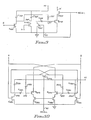
- FIG. 5 depicts a schematic diagram of a still further improved embodiment of the invention as it would be applied to improve the circuit of Figure 3.
- Level shifter 66 has been added to the original circuit of Figure 3 and connected as shown with its input terminal connected to D , its power supply terminal connected to HV and its output terminal connected to FN 20. This circuit further departs from that of Figures 1 and 3 in that FN 22 of those Figures has been deleted. The upper end of FN 20 is no longer connected directly to high voltage node HV, but, rather, is connected to the output of level shifter 66.
- Level shifter 68 replaces level shifter 41 of Figures 3 and 3A to the extent that it is connected to the left end of capacitor C26 at node 54.
- D and D To effect a net positive charge on node 32, D and D must be at high and low levels, respectively, as before.
- the high voltage HV appears at the output of level shifter 66 and electron tunneling occurs in FN20 as before.
- the D and D inputs are set to the opposite states, as before.
- High voltage then appears at node 54 via level shifter 68, and node 32, being closely coupled to node 54, rises with the high voltage at nodes HV and 54.
- Level shifter 66 with a high level at its input holds the upper end of FN 20 at ground potential.
- Tunneling element 22 of Figure 3 is no longer necessary and is deleted. Since charge and discharge of the floating gate device Q24 is accomplished by drawing both charge and discharge current through FN 20 in both directions, the "walkout" effect in that device is significantly reduced.
- Figure 6 is a schematic diagram of an implementation of the embodiment of the invention of Figure 5, as applied to the differential circuit of Figures 2 and 4.
- the device count is again reduced because of the dual functions of the level shifters 68A and 68B, eliminating the need for the equivalent clrcuit of level shifter 66, and the elimination of half of the FN devices, 22A and 22B as shown in Figures 2 and 4.
- Figures 7 and 8 illustrate, respectively, the circuits of Figures 5 and 6, as implemented in P-well CMOS technology.
- the like reference numerals carry a "C" suffix in Figure 7 and "D” and "E” suffixes in Figure 8.
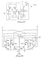
- FIGS 9 and 10 respectively, illustrate the circuits of Figures 5 and 6 as implemented in NMOS with N-channel devices; there are no P-channel devices employed.
- Capacitors C70 and C72 have been added for this implementation. While like reference numerals are used, they carry an "F" suffix in Figure 9 and "G” and "H” suffixes in Figure 10.
- Figures 11 and 12 are illustrative of the circuits of Figures 5 and 6, respectively, as they are implemented in N-well CMOS technology. It should be noted that the same reference numerals are used to identify those elements of the circuits which perform the functions of those same reference numeraled elements of Figures 4, 5 and 6, but they carry a "K" suffix in Figure 11 and "L” and "M” suffixes in Figure 12.
- Figure 13 is a detailed schematic diagram of an embodiment of the invention in N-well CMOS technology as applied to a single ended cell in the prior art circuit of Figure 1 wherein elements carrying like reference numerals perform the same function as that of the other elements disclosed in the various drawings of this disclosure.
- Figure 14 is a detailed schematic diagram of the embodiment of the invention as shown in Figure 13, but as applied to a differential cell, as shown in Figure 2.
- the "A" and "B" suffixes identify the duplicate elements required for the differential version of the circuit.
- Figure 15 is a detailed schematic diagram of an alternative embodiment of the invention of Figure 13 as it is implemented in P-well CMOS technology. Again, like reference numerals identify elements which perform similar functions to those of Figure 13.
- Figure 16 is a detailed schematic diagram of an alternative embodiment of the invention of Figure 14 as it is implemented in P-well CMOS technology. Like reference numerals identify elements which perform functions similar to those of Figure 14.
Landscapes
- Read Only Memory (AREA)
- Non-Volatile Memory (AREA)
Applications Claiming Priority (2)
| Application Number | Priority Date | Filing Date | Title |
|---|---|---|---|
| US81037 | 1987-08-03 | ||
| US07/081,037 US4787066A (en) | 1987-08-03 | 1987-08-03 | Non-volatile shadow storage cell with improved level shifting circuit and reduced tunnel device count for improved reliability |
Publications (3)
| Publication Number | Publication Date |
|---|---|
| EP0302779A2 true EP0302779A2 (de) | 1989-02-08 |
| EP0302779A3 EP0302779A3 (en) | 1990-10-31 |
| EP0302779B1 EP0302779B1 (de) | 1993-05-26 |
Family
ID=22161716
Family Applications (1)
| Application Number | Title | Priority Date | Filing Date |
|---|---|---|---|
| EP88401990A Expired - Lifetime EP0302779B1 (de) | 1987-08-03 | 1988-07-29 | Nichtflüchtige latente Speicherzelle mit Pegelumformerschaltung und reduzierter Tunneleffektschaltung für verbesserte Betriebssicherheit |
Country Status (4)
| Country | Link |
|---|---|
| US (1) | US4787066A (de) |
| EP (1) | EP0302779B1 (de) |
| JP (1) | JP3080624B2 (de) |
| DE (1) | DE3881296T2 (de) |
Families Citing this family (7)
| Publication number | Priority date | Publication date | Assignee | Title |
|---|---|---|---|---|
| US5434811A (en) * | 1987-11-19 | 1995-07-18 | National Semiconductor Corporation | Non-destructive read ferroelectric based memory circuit |
| US5185721A (en) * | 1988-10-31 | 1993-02-09 | Texas Instruments Incorporated | Charge-retaining signal boosting circuit and method |
| US5202855A (en) * | 1991-01-14 | 1993-04-13 | Motorola, Inc. | DRAM with a controlled boosted voltage level shifting driver |
| JPH06236694A (ja) * | 1991-05-07 | 1994-08-23 | Intel Corp | 高電圧レベル変換回路 |
| KR940010837B1 (ko) * | 1991-10-21 | 1994-11-17 | 현대전자산업 주식회사 | Dram의 워드선 구동회로 |
| US5563831A (en) * | 1995-08-30 | 1996-10-08 | Etron Technology Inc. | Timing reference circuit for bitline precharge in memory arrays |
| US9613714B1 (en) * | 2016-01-19 | 2017-04-04 | Ememory Technology Inc. | One time programming memory cell and memory array for physically unclonable function technology and associated random code generating method |
Family Cites Families (5)
| Publication number | Priority date | Publication date | Assignee | Title |
|---|---|---|---|---|
| JPS54150955A (en) * | 1978-05-18 | 1979-11-27 | Mitsubishi Electric Corp | Voltage converter circuit |
| US4510584A (en) * | 1982-12-29 | 1985-04-09 | Mostek Corporation | MOS Random access memory cell with nonvolatile storage |
| IT1212765B (it) * | 1983-07-27 | 1989-11-30 | Ates Componenti Elettron | Cella di memoria di tipo ram con elemento di memoria non volatile elettricamente programmabile. |
| JPS6083374A (ja) * | 1983-10-14 | 1985-05-11 | Fujitsu Ltd | 半導体記憶装置 |
| US4685083A (en) * | 1985-10-03 | 1987-08-04 | Thomson Components-Mostek Corporation | Improved nonvolatile memory circuit using a dual node floating gate memory cell |
-
1987
- 1987-08-03 US US07/081,037 patent/US4787066A/en not_active Expired - Lifetime
-
1988
- 1988-07-29 DE DE8888401990T patent/DE3881296T2/de not_active Expired - Fee Related
- 1988-07-29 EP EP88401990A patent/EP0302779B1/de not_active Expired - Lifetime
- 1988-08-03 JP JP19428888A patent/JP3080624B2/ja not_active Expired - Fee Related
Also Published As
| Publication number | Publication date |
|---|---|
| EP0302779A3 (en) | 1990-10-31 |
| JPH01112595A (ja) | 1989-05-01 |
| JP3080624B2 (ja) | 2000-08-28 |
| US4787066A (en) | 1988-11-22 |
| EP0302779B1 (de) | 1993-05-26 |
| DE3881296D1 (de) | 1993-07-01 |
| DE3881296T2 (de) | 1993-09-09 |
Similar Documents
| Publication | Publication Date | Title |
|---|---|---|
| EP0467928B1 (de) | Novramzell unter verwendung von zwei differentialen entkopplungsbaren nichtflüchtigen speicherelementen | |
| US4510584A (en) | MOS Random access memory cell with nonvolatile storage | |
| US5422590A (en) | High voltage negative charge pump with low voltage CMOS transistors | |
| AU564114B2 (en) | Nonvolatile latch | |
| EP0840930B1 (de) | Programmierbarer nichtflüchtiger zweiwegschalter für programmierbare logik | |
| US4866307A (en) | Integrated programmable bit circuit using single-level poly construction | |
| JP2585348B2 (ja) | 不揮発性半導体記憶装置 | |
| US4733371A (en) | Semiconductor memory device with high voltage switch | |
| EP0616368B1 (de) | Nichtflüchtiges Halbleiterspeicherbauelement, welches die Anforderungen an dessen Spannungsfestigkeit verringert | |
| US7339821B2 (en) | Dual-gate nonvolatile memory and method of program inhibition | |
| US5506518A (en) | Antifuse-based programmable logic circuit | |
| US6023427A (en) | Voltage pump switch | |
| US4787066A (en) | Non-volatile shadow storage cell with improved level shifting circuit and reduced tunnel device count for improved reliability | |
| EP0302780B1 (de) | Nichtflüchtige latente Speicherzelle mit reduzierter Tunneleffektschaltung für verbesserte Betriebssicherheit | |
| JP4328390B2 (ja) | 不揮発性レジスタおよびデ−タにアクセスする方法 | |
| JPH02199698A (ja) | 半導体集積回路 | |
| JPS6237472B2 (de) | ||
| EP0654791B1 (de) | Nicht-flüchtige Speicheranordnung mit Mitteln zur Erzeugung negativer Programmierspannungen | |
| EP0377841B1 (de) | Integrierte Halbleiterschaltung, fähig ein Ereignis einer fehlerhaften Wirkung wegen Störungen zu verhindern | |
| US5327392A (en) | Semiconductor integrated circuit capable of preventing occurrence of erroneous operation due to noise | |
| JPH0715796B2 (ja) | 不揮発性ramメモリセル | |
| JP2677747B2 (ja) | 高電圧スイッチ回路 | |
| EP0475066A2 (de) | EEPROM Analogschalter | |
| WO1990015412A1 (en) | A high reliability non-volatile memory circuit and structure | |
| US4475177A (en) | Non-volatile semiconductor memory circuits |
Legal Events
| Date | Code | Title | Description |
|---|---|---|---|
| PUAI | Public reference made under article 153(3) epc to a published international application that has entered the european phase |
Free format text: ORIGINAL CODE: 0009012 |
|
| AK | Designated contracting states |
Kind code of ref document: A2 Designated state(s): DE FR IT |
|
| PUAL | Search report despatched |
Free format text: ORIGINAL CODE: 0009013 |
|
| AK | Designated contracting states |
Kind code of ref document: A3 Designated state(s): DE FR IT |
|
| 17P | Request for examination filed |
Effective date: 19901205 |
|
| 17Q | First examination report despatched |
Effective date: 19920520 |
|
| GRAA | (expected) grant |
Free format text: ORIGINAL CODE: 0009210 |
|
| AK | Designated contracting states |
Kind code of ref document: B1 Designated state(s): DE FR IT |
|
| ITF | It: translation for a ep patent filed | ||
| REF | Corresponds to: |
Ref document number: 3881296 Country of ref document: DE Date of ref document: 19930701 |
|
| ET | Fr: translation filed | ||
| PLBE | No opposition filed within time limit |
Free format text: ORIGINAL CODE: 0009261 |
|
| STAA | Information on the status of an ep patent application or granted ep patent |
Free format text: STATUS: NO OPPOSITION FILED WITHIN TIME LIMIT |
|
| 26N | No opposition filed | ||
| PGFP | Annual fee paid to national office [announced via postgrant information from national office to epo] |
Ref country code: FR Payment date: 19980709 Year of fee payment: 11 |
|
| PGFP | Annual fee paid to national office [announced via postgrant information from national office to epo] |
Ref country code: DE Payment date: 19980810 Year of fee payment: 11 |
|
| PG25 | Lapsed in a contracting state [announced via postgrant information from national office to epo] |
Ref country code: FR Free format text: THE PATENT HAS BEEN ANNULLED BY A DECISION OF A NATIONAL AUTHORITY Effective date: 19990731 |
|
| PG25 | Lapsed in a contracting state [announced via postgrant information from national office to epo] |
Ref country code: DE Free format text: LAPSE BECAUSE OF NON-PAYMENT OF DUE FEES Effective date: 20000503 |
|
| REG | Reference to a national code |
Ref country code: FR Ref legal event code: ST |
|
| PG25 | Lapsed in a contracting state [announced via postgrant information from national office to epo] |
Ref country code: IT Free format text: LAPSE BECAUSE OF NON-PAYMENT OF DUE FEES;WARNING: LAPSES OF ITALIAN PATENTS WITH EFFECTIVE DATE BEFORE 2007 MAY HAVE OCCURRED AT ANY TIME BEFORE 2007. THE CORRECT EFFECTIVE DATE MAY BE DIFFERENT FROM THE ONE RECORDED. Effective date: 20050729 |