EP0301703B1 - Display control system - Google Patents
Display control system Download PDFInfo
- Publication number
- EP0301703B1 EP0301703B1 EP88305829A EP88305829A EP0301703B1 EP 0301703 B1 EP0301703 B1 EP 0301703B1 EP 88305829 A EP88305829 A EP 88305829A EP 88305829 A EP88305829 A EP 88305829A EP 0301703 B1 EP0301703 B1 EP 0301703B1
- Authority
- EP
- European Patent Office
- Prior art keywords
- display
- window
- memory
- image data
- mode
- Prior art date
- Legal status (The legal status is an assumption and is not a legal conclusion. Google has not performed a legal analysis and makes no representation as to the accuracy of the status listed.)
- Expired - Lifetime
Links
Images


Classifications
-
- G—PHYSICS
- G09—EDUCATION; CRYPTOGRAPHY; DISPLAY; ADVERTISING; SEALS
- G09G—ARRANGEMENTS OR CIRCUITS FOR CONTROL OF INDICATING DEVICES USING STATIC MEANS TO PRESENT VARIABLE INFORMATION
- G09G5/00—Control arrangements or circuits for visual indicators common to cathode-ray tube indicators and other visual indicators
- G09G5/14—Display of multiple viewports
Definitions
- image display is controlled by one of the following systems shown in Figs. 5(a), (b) and (c).
- a window controller 14 allows the content of the window buffer memory 12 to be displayed directly with no intervention of the display memory 11, at a desired position overlapping the content of the display memory 11 on the display screen. This display position control is achieved by writing the status related to display in the register in the window controller 14.
- a selection circuit 15 selects the direct access display mode in which the content of the window buffer memory 12 is displayed directly on the display device or the graphic drawing mode in which the window buffer memory content is not displayed on the display device. When the direct access display mode is selected, the operation timing of the window buffer memory 12 is shared between the display cycle in which the window controller 14 makes access to the window buffer memory 12 and the graphic drawing cycle in which the graphic controller 13 makes access to the window buffer memory 12 via the bus line 18.
- the display control system comprises a display memory having a random access port and a serial access port, a window buffer memory for storing image data, a window controller for controlling the position of the window buffer memory content displayed on a display device, and a selection circuit for setting the operation mode of the window buffer memory to the direct access display mode or to the graphic drawing mode.
- the direct access display mode is selected, the window buffer memory content is presented directly on the display device in shared time as the position of the data displayed is controlled by the window controller.
- the graphic drawing mode image data transmission between the window buffer memory and the display memory or graphic drawing in the window buffer memory is conducted without time sharing.
Landscapes
- Engineering & Computer Science (AREA)
- Physics & Mathematics (AREA)
- Computer Hardware Design (AREA)
- General Physics & Mathematics (AREA)
- Theoretical Computer Science (AREA)
- Digital Computer Display Output (AREA)
- Image Generation (AREA)
- Controls And Circuits For Display Device (AREA)
Description
- This invention relates to a display control system.
- Conventionally, image display is controlled by one of the following systems shown in Figs. 5(a), (b) and (c).
- The display control system shown in Fig. 5(a) is a so-called software window system involving raster operation. In this system, the image data of the windows A, B and C stored in a window memory 1 are transferred in blocks to a
display memory 2 through raster operation so that picture editing such as positioning and superposing of the windows A, B and C are performed in thedisplay memory 2. After editing the image data are read sequentially from thedisplay memory 2 for multi-window display on aCRT 3. - The display control system shown in Fig. 5(b) is a so-called hardware window system involving a mapping table. In this system, the address of the image data corresponding to the current scanning position on a
CRT 6 is output sequentially from a hardware mapping table 5 during scanning operation by theCRT 6, and the image data of the windows A, B and C stored in awindow memory 4 are read in shared time according to the above address and output directly to theCRT 6 for multi-window display. - The display control system shown in Fig. 5(c) is so-called a software window system involving clipping. In this system, a picture is drawn in a
display memory 8 using the code data for the image information of the windows A, B and C stored in asegment buffer 7 after clipping the code data of the image information outside the windows. The image data is then read sequentially from thedisplay memory 8 for multi-window display on a CRT 9. - The above conventional display control systems of Figs. (a), (b) and (c) have disadvantages, respectively.
- The disadvantage of the display control system of (a) involving raster operation is as follows. The image data in the window memory 1 must be transferred in blocks to the
display memory 2 to edit a picture in thedisplay memory 2 before the picture is displayed on theCRT 3. This operation must be carried out every time the window is moved on the CRT 3. Therefore, the window cannot be moved quickly. - The disadvantage of the system of (b) involving a mapping table is as follows. The addresses of the image data in the
window memory 4 are output sequentially from the mapping table 5 so that the image data stored at the addresses are read in shared time and displayed directly on theCRT 6. With this system, it is possible to move the window quickly. On the other hand, however, since graphic drawing in thewindow memory 4 is also performed in shared time, drawing speed is slow. - The disadvantage of the system of (c) involving clipping is as follows. The code data of unnecessary image data in the
segment buffer 7 is removed by clipping before the code data of the image data stored in thesegment buffer 7 is transferred for graphic drawing on thedisplay memory 8 and displayed on the CRT 9. To move the window on the CRT 9, therefore, the system requires a hardware for drawing graphics at a high speed on thedisplay memory 8 from the code data stored in thesegment buffer 7. - A further example of prior art window systems is disclosed in EP-A-O 153 197, in which data has to be first written to screen buffers before being output to a screen.
- In order to alleviate at least some of the problems encountered in the prior art the present invention provides a display control system having:
a full screen display memory for providing image data for display by a display device;
a window memory for storing alphanumeric and/or graphic window image data defining one or more image portions to be displayed by the display device;
first control means operable to selectively move the display position of the image portion or portions; and
second control means for controlling the supply of image data and window image data to the display device, said second control means being operable in a direct access display mode of the system to cause window image data to be supplied direct from the window memory and image data to be supplied from the display memory, the window position being changeable in said direct access display mode by operation of said first control means, the system also being operable in a graphic drawing mode to permit data drawing and editing in the window memory. - An advantage of the present invention is that in the direct access display mode it is possible to move the window on the display quickly while watching the screen and, in the graphic drawing mode it is possible to draw and edit graphics rapidly in the window memory, thus allowing the operator to edit a document at a high speed while watching the CRT screen.
- The present invention will become more fully understood from the detailed description given hereinbelow and the accompanying drawings which are given by way of illustration only, and thus are not limitative of the present invention and wherein:
- Fig. 1 is a block diagram of an embodiment of the present invention;
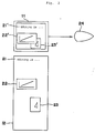
- Fig. 2 is a diagram for explaining the document editing by the embodiment of Fig. 1;
- Fig. 3 is a block diagram of another embodiment of the present invention;
- Fig. 4 is a block diagram of still another embodiment of the present invention; and
- Figs. 5(a) to (c) are diagrams for explaining the conventional display control systems.
- To display window buffer memory content directly on a display device overlapping display memory content, a selection circuit is set for the direct access display mode. Then, the operation timing of the window buffer memory is shared between the direct access display cycle and the graphic drawing cycle, so that window buffer memory content is displayed directly over the display memory content on the screen of the display device as the position of the window buffer memory content displayed is controlled by a window controller. Thus, in the direct access display mode, a window can be moved rapidly on the display screen. When window buffer memory content is not to be displayed directly on the display device, the selection circuit is set for the graphic drawing mode. Then, the operation timing of the window buffer memory is used solely for the graphic drawing cycle so that graphics are drawn and edited in the window buffer memory and display memory. Accordingly, in the graphic drawing mode, it is possible to draw graphics and edit display data in the window buffer memory and display memory at a high speed.
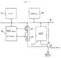
- Fig. 1 is a block diagram of an embodiment of the present invention. A
display memory 11 is a bit map memory for display having memory elements corresponding to the picture elements on the display device. Thedisplay memory 11 is provided with a serial access port for sending data to the display device and a random access port for data communication with a graphic drawing device. - A
window buffer memory 12 is designed to store image data such as sentences, figures and tables. In this embodiment, thewindow buffer memory 12 also serves as a main memory for effective use of the memory. This feature has a demerit that aCPU 17 cannot make access to the main memory while agraphic controller 13 is making access to thewindow buffer memory 12. On the other hand, however, this feature permits the effective use of thewindow buffer memory 12 whose capacity increases with the amount of image data to be displayed. Thegraphic controller 13 transmits image data between thewindow buffer memory 12 and thedisplay memory 11 via abus line 18 or draws graphics on both memories. - A
window controller 14 allows the content of thewindow buffer memory 12 to be displayed directly with no intervention of thedisplay memory 11, at a desired position overlapping the content of thedisplay memory 11 on the display screen. This display position control is achieved by writing the status related to display in the register in thewindow controller 14. Aselection circuit 15 selects the direct access display mode in which the content of thewindow buffer memory 12 is displayed directly on the display device or the graphic drawing mode in which the window buffer memory content is not displayed on the display device. When the direct access display mode is selected, the operation timing of thewindow buffer memory 12 is shared between the display cycle in which thewindow controller 14 makes access to thewindow buffer memory 12 and the graphic drawing cycle in which thegraphic controller 13 makes access to thewindow buffer memory 12 via thebus line 18. When the graphic drawing mode is selected, the operation timing of thewindow buffer memory 12 is used only by the graphic drawing cycle so that thewindow buffer memory 12 is used 100% by thegraphic controller 13. Araster operation circuit 16 sends image data output from thedisplay memory 11 and image data output from thewindow controller 14 to the display device such as a CRT after logical operation. - In the following description of the operation of the present embodiment, it is assumed that the
window buffer memory 12 has stored the image data ofsentences 21, agraphic chart 22 and a figure 23 as shown in Fig. 2. - When the operator is to move the
graphic chart 22 and the figure 23 to appropriate positions overlapping thesentences 21 on the display screen of theCRT 24 in real time while watching the picture on the screen and, draw the image data with thegraphic chart 22 and the figure 23 fixed at their most appropriate positions, on thedisplay memory 11, he operates the system as follows. - The
selection circuit 15 is set for the graphic drawing mode so that the operation timing of thewindow buffer memory 12 is used for graphic drawing cycle alone. With this setting, thedisplay memory 11 which is a two-port memory can use about 97% of the cycle time for transferring image data while thewindow buffer memory 12 can use 100% of the cycle time for transferring image data. Accordingly, image data can be transferred in blocks at a high speed by thegraphic controller 13. As a result, the image data of thesentences 21 in thewindow buffer memory 12 is transferred to thedisplay memory 11 at a high speed. - To enable the operator to move the
graphic chart 22 and the figure 23 in real time while watching the picture on theCRT 24, theselection circuit 15 is switched over for the direct access display mode so that the operation timing of thewindow buffer memory 12 is shared between the direct access display cycle and the graphic drawing cycle. In the direct access display cycle, thewindow controller 14 accesses the address of thewindow buffer memory 12 calculated according to the display status written in the internal register to read the image data of thegraphic chart 22 or figure 23 and outputs the image data directly to theraster operation circuit 16 rapidly with no intervention of thedisplay memory 11. Neanwhile, the image data of thesentences 21 already transferred from thewindow buffer memory 12 is output through the serial access part of thedisplay memory 11. Theraster operation circuit 16 executes logical operation for the image data of thesentences 21 output from thedisplay memory 11 and for the image data of thegraphic chart 22 and figure 23 output from thewindow buffer memory 12, and outputs the image data of thegraphic chart 22 and figure 23 overlapping thesentences 21 to theCRT 24. At this time, the display positions of thegraphic chart 22 and figure 23 can be changed quickly by changing the display status written in the register of thewindow controller 14. - Since the operation timing of the
window buffer memory 12 is time shared between the graphic drawing cycle and direct access display cycle, it is possible to draw graphics in thewindow buffer memory 12 when the operation timing is for the graphic drawing cycle. It must be noted, however, that the graphic drawing speed in this mode is slower than that in the graphic drawing mode (in which the operation timing is used only for the graphic drawing cycle). - When the
graphic chart 22 and the figure 23 have been positioned on the display screen of theCRT 24, theselection circuit 15 is switched over for the graphic drawing mode so that the operation timing of thewindow buffer memory 12 can be used solely for the graphic drawing cycle. Then, the image data of thegraphic chart 22 and figure 23 thus positioned is transferred at a high speed from thewindow buffer memory 12 to the specified address in thedisplay memory 11 under the control by thegraphic controller 13. As a result, the image data for a picture with agraphic chart 22' and a figure 23' overlapping with sentences 21' as shown in Fig. 2 is formed in thedisplay memory 11. - According to the above embodiment of the invention, as mentioned above, the direct access display mode or the graphic drawing mode is selected by the
selection circuit 15. In the direct access display mode, the operation timing of thewindow buffer memory 12 is time shared between the direct access display cycle and the graphic drawing cycle so that thewindow controller 14 transfers the content of thewindow buffer memory 12 directly to theCRT 24, presenting an active window display at a high speed. In the graphic drawing mode, the operation timing of thewindow buffer memory 12 is used for the graphic drawing cycle alone so that data drawing and editing in thewindow buffer memory 12 can be conducted rapidly. As a result, the operator can edit document rapidly while watching the picture on theCRT 24. - Fig. 3 shows another embodiment in which a
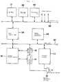
window buffer memory 31 is used only for storing image data and a RAM (random access memory) 32 is provided separately as a main memory. Bus line comprises animage bus 37 for transmitting image data and aninternal bus 36. Thewindow buffer memory 31, theselection circuit 15, thewindow controller 14, thedisplay memory 11 and animage editing processor 33 are connected with theimage bus 37. A FIFO two-port RAM 34 is connected between theimage bus 37 and theinternal bus 36. Theimage bus 37 or theinternal bus 36 is selected by the FIFO two-port RAM 34 to present an image display at a high speed. - Fig. 4 shows still another embodiment of the invention in which image data transfer between the
window buffer memory 12 and thedisplay memory 11 or graphic drawing in thewindow buffer memory 12 or thedisplay memory 11 is executed by aCPU 41. - According to the above embodiment of the present invention, the display control system comprises a display memory having a random access port and a serial access port, a window buffer memory for storing image data, a window controller for controlling the position of the window buffer memory content displayed on a display device, and a selection circuit for setting the operation mode of the window buffer memory to the direct access display mode or to the graphic drawing mode. When the direct access display mode is selected, the window buffer memory content is presented directly on the display device in shared time as the position of the data displayed is controlled by the window controller. When the graphic drawing mode is selected, image data transmission between the window buffer memory and the display memory or graphic drawing in the window buffer memory is conducted without time sharing. Consequently, it is possible for an operator to move a window at a high speed while watching the picture on the CRT when the selection circuit is switched over for the display mode, and to draw and edit graphics in the window buffer memory at a high speed when the selection circuit is switched over for the graphic drawing mode. As a result, it is possible to edit a document actively and rapidly while watching the picture on the display device.
- While only certain embodiments of the present invention have been described, it will be apparent to those skilled in the art that various changes and modifications may be made therein without departing from the scope of the present invention as claimed.
Claims (4)
- A display control system having:
a full screen display memory (11) for providing image data for display by a display device;
a window memory (12;31) for storing alphanumeric and/or graphic window image data defining one or more image portions to be displayed by the display device;
first control means (14) operable to selectively move the display position of the image portion or portions; and
second control means (15,16) for controlling the supply of image data and window image data to the display device, said second control means (15,16) being operable in a direct access display mode of the system to cause window image data to be supplied direct from the window memory (12;31) and image data to be supplied from the display memory (11), the window position being changeable in said direct access display mode by operation of said first control means (14), the system also being operable in a graphic drawing mode to permit data drawing and editing in the window memory (12;31). - A display control system as claimed in claim 1, wherein:
said display memory (11) comprises a serial access port for sending data to said display device and a random access port for data communication with a graphic drawing device;
said first control means comprises a window controller (14) for controlling the position of the contents of the window memory (12;31) displayed on the display device; and
said second control means comprises a raster operation circuit (16) and a selection circuit (15) for selecting said direct access display mode or said graphic drawing mode. - A display control system as claimed in claim 2, wherein the selection circuit is switched over for the direct access display mode when the contents of the window memory (12;31) are to be transferred directly to the display device so as to be displayed overlapping with the contents of the display memory (11), and for the graphic drawing mode when the contents of the window memory (12; 31) are not to be displayed directly on the display device.
- A display control system as claimed in claim 1 or claim 2, wherein in the direct access display mode, the contents of the window memory (12;31) are displayed directly on the display device in shared time with graphic drawing in the window memory (12;31), and wherein, in the graphic drawing mode, image data transmission between the window memory (12;31) and the display memory (11) or graphic drawing in the window memory (12;31) is carried out without time sharing.
Applications Claiming Priority (2)
| Application Number | Priority Date | Filing Date | Title |
|---|---|---|---|
| JP160574/87 | 1987-06-26 | ||
| JP62160574A JPS644828A (en) | 1987-06-26 | 1987-06-26 | Image display control system |
Publications (3)
| Publication Number | Publication Date |
|---|---|
| EP0301703A2 EP0301703A2 (en) | 1989-02-01 |
| EP0301703A3 EP0301703A3 (en) | 1990-01-10 |
| EP0301703B1 true EP0301703B1 (en) | 1994-08-31 |
Family
ID=15717908
Family Applications (1)
| Application Number | Title | Priority Date | Filing Date |
|---|---|---|---|
| EP88305829A Expired - Lifetime EP0301703B1 (en) | 1987-06-26 | 1988-06-27 | Display control system |
Country Status (4)
| Country | Link |
|---|---|
| US (1) | US4959803A (en) |
| EP (1) | EP0301703B1 (en) |
| JP (1) | JPS644828A (en) |
| DE (1) | DE3851285T2 (en) |
Families Citing this family (25)
| Publication number | Priority date | Publication date | Assignee | Title |
|---|---|---|---|---|
| KR910003742B1 (en) * | 1986-09-09 | 1991-06-10 | 세미콘덕터 에너지 라보라터리 캄파니 리미티드 | Cvd apparatus |
| US5061919A (en) * | 1987-06-29 | 1991-10-29 | Evans & Sutherland Computer Corp. | Computer graphics dynamic control system |
| US5387945A (en) * | 1988-07-13 | 1995-02-07 | Seiko Epson Corporation | Video multiplexing system for superimposition of scalable video streams upon a background video data stream |
| JP2748562B2 (en) | 1988-07-13 | 1998-05-06 | セイコーエプソン株式会社 | Image processing device |
| JPH03264215A (en) * | 1990-02-13 | 1991-11-25 | Mitsubishi Electric Corp | Numerical control unit for electric discharge machine |
| US5371877A (en) * | 1991-12-31 | 1994-12-06 | Apple Computer, Inc. | Apparatus for alternatively accessing single port random access memories to implement dual port first-in first-out memory |
| US5319388A (en) * | 1992-06-22 | 1994-06-07 | Vlsi Technology, Inc. | VGA controlled having frame buffer memory arbitration and method therefor |
| US5361081A (en) * | 1993-04-29 | 1994-11-01 | Digital Equipment Corporation | Programmable pixel and scan-line offsets for a hardware cursor |
| US5638501A (en) | 1993-05-10 | 1997-06-10 | Apple Computer, Inc. | Method and apparatus for displaying an overlay image |
| WO1995025997A1 (en) * | 1994-03-23 | 1995-09-28 | Igor Anatolievich Terehov | Pulse shaper for producing pulses controlling the formation of a discrete raster on the screen of a cathode ray tube |
| JP3492761B2 (en) * | 1994-04-07 | 2004-02-03 | 株式会社ソニー・コンピュータエンタテインメント | Image generation method and apparatus |
| RU2094951C1 (en) * | 1995-03-21 | 1997-10-27 | Игорь Анатольевич Терехов | Generator of information sampling pulses for cathode-ray tube screen |
| RU2094952C1 (en) * | 1995-05-22 | 1997-10-27 | Игорь Анатольевич Терехов | Generator of information sampling pulses for cathode-ray tube screen |
| US6029160A (en) * | 1995-05-24 | 2000-02-22 | International Business Machines Corporation | Method and means for linking a database system with a system for filing data |
| US5854637A (en) | 1995-08-17 | 1998-12-29 | Intel Corporation | Method and apparatus for managing access to a computer system memory shared by a graphics controller and a memory controller |
| US5818464A (en) * | 1995-08-17 | 1998-10-06 | Intel Corporation | Method and apparatus for arbitrating access requests to a shared computer system memory by a graphics controller and memory controller |
| DE59712964D1 (en) * | 1996-03-25 | 2008-10-23 | Micronas Gmbh | Circuit arrangement for picture-in-picture insertion |
| US9189467B1 (en) | 2001-11-07 | 2015-11-17 | Apple Inc. | Method and apparatus for annotating an electronic document |
| US20070039027A1 (en) * | 2005-07-22 | 2007-02-15 | Sony Corporation | RF based display control system |
| EP2104930A2 (en) | 2006-12-12 | 2009-09-30 | Evans & Sutherland Computer Corporation | System and method for aligning rgb light in a single modulator projector |
| US8358317B2 (en) | 2008-05-23 | 2013-01-22 | Evans & Sutherland Computer Corporation | System and method for displaying a planar image on a curved surface |
| US8702248B1 (en) | 2008-06-11 | 2014-04-22 | Evans & Sutherland Computer Corporation | Projection method for reducing interpixel gaps on a viewing surface |
| US8077378B1 (en) | 2008-11-12 | 2011-12-13 | Evans & Sutherland Computer Corporation | Calibration system and method for light modulation device |
| US9092128B2 (en) | 2010-05-21 | 2015-07-28 | Apple Inc. | Method and apparatus for managing visual information |
| US9641826B1 (en) | 2011-10-06 | 2017-05-02 | Evans & Sutherland Computer Corporation | System and method for displaying distant 3-D stereo on a dome surface |
Family Cites Families (11)
| Publication number | Priority date | Publication date | Assignee | Title |
|---|---|---|---|---|
| US3792462A (en) * | 1971-09-08 | 1974-02-12 | Bunker Ramo | Method and apparatus for controlling a multi-mode segmented display |
| US4412294A (en) * | 1981-02-23 | 1983-10-25 | Texas Instruments Incorporated | Display system with multiple scrolling regions |
| JPS59116787A (en) * | 1982-12-24 | 1984-07-05 | 株式会社日立製作所 | Display indication system |
| DE3381300D1 (en) * | 1983-03-31 | 1990-04-12 | Ibm | IMAGE ROOM MANAGEMENT AND PLAYBACK IN A PART OF THE SCREEN OF A VIRTUAL MULTIFUNCTIONAL TERMINAL. |
| US4542376A (en) * | 1983-11-03 | 1985-09-17 | Burroughs Corporation | System for electronically displaying portions of several different images on a CRT screen through respective prioritized viewports |
| US4663617A (en) * | 1984-02-21 | 1987-05-05 | International Business Machines | Graphics image relocation for display viewporting and pel scrolling |
| US4714918A (en) * | 1984-04-30 | 1987-12-22 | International Business Machines Corporation | Window view control |
| US4633415A (en) * | 1984-06-11 | 1986-12-30 | Northern Telecom Limited | Windowing and scrolling for a cathode-ray tube display |
| JPS6177977A (en) * | 1984-09-25 | 1986-04-21 | Canon Inc | Picture processor |
| US4700320A (en) * | 1985-07-09 | 1987-10-13 | American Telephone And Telegraph Company, At&T Bell Laboratories | Bitmapped graphics workstation |
| US4860218A (en) * | 1985-09-18 | 1989-08-22 | Michael Sleator | Display with windowing capability by addressing |
-
1987
- 1987-06-26 JP JP62160574A patent/JPS644828A/en active Granted
-
1988
- 1988-06-24 US US07/210,855 patent/US4959803A/en not_active Expired - Lifetime
- 1988-06-27 EP EP88305829A patent/EP0301703B1/en not_active Expired - Lifetime
- 1988-06-27 DE DE3851285T patent/DE3851285T2/en not_active Expired - Lifetime
Non-Patent Citations (1)
| Title |
|---|
| PATENT ABSTRACTS OF JAPAN vol. 10, no. 250 (P-491)(2306), 28 August 1986 & JP-A-61 077977 * |
Also Published As
| Publication number | Publication date |
|---|---|
| DE3851285T2 (en) | 1995-03-09 |
| DE3851285D1 (en) | 1994-10-06 |
| JPH0468655B2 (en) | 1992-11-04 |
| US4959803A (en) | 1990-09-25 |
| JPS644828A (en) | 1989-01-10 |
| EP0301703A2 (en) | 1989-02-01 |
| EP0301703A3 (en) | 1990-01-10 |
Similar Documents
| Publication | Publication Date | Title |
|---|---|---|
| EP0301703B1 (en) | Display control system | |
| US5299309A (en) | Fast graphics control system capable of simultaneously storing and executing graphics commands | |
| KR920001958B1 (en) | Graphic display system | |
| JPS60112095A (en) | Method and apparatus for renewing image for computer displayunit | |
| US5774132A (en) | Video capture computer system using local memory for texture mapping | |
| US5313227A (en) | Graphic display system capable of cutting out partial images | |
| US6005572A (en) | Display unit having plurality of frame buffers | |
| US4748442A (en) | Visual displaying | |
| JPH08278778A (en) | Method and apparatus for display control of image | |
| EP0803798A1 (en) | System for use in a computerized imaging system to efficiently transfer graphics information to a graphics subsystem employing masked direct frame buffer access | |
| EP0337752B1 (en) | Graphic display system for cutting out partial image | |
| JP2555325B2 (en) | Display device | |
| JPS6159484A (en) | Segment control system | |
| JP3093228B2 (en) | Image processing apparatus and method | |
| JPH02114294A (en) | Graphic display device | |
| JPH0227677B2 (en) | ||
| JP2000231473A (en) | Display controller and method for data transfer to display | |
| JPH02132566A (en) | Image data transferring device | |
| JPS63245716A (en) | Multiwindow display device | |
| JPS62138971A (en) | Data processor | |
| JPS60108882A (en) | Fast editing display | |
| JPH03144692A (en) | Transfer system for rectangular area image data | |
| JPH01142789A (en) | Hard copy control system | |
| JPH01121893A (en) | Graphic display device | |
| JPH04199284A (en) | Display device |
Legal Events
| Date | Code | Title | Description |
|---|---|---|---|
| PUAI | Public reference made under article 153(3) epc to a published international application that has entered the european phase |
Free format text: ORIGINAL CODE: 0009012 |
|
| AK | Designated contracting states |
Kind code of ref document: A2 Designated state(s): DE GB |
|
| PUAL | Search report despatched |
Free format text: ORIGINAL CODE: 0009013 |
|
| AK | Designated contracting states |
Kind code of ref document: A3 Designated state(s): DE GB |
|
| 17P | Request for examination filed |
Effective date: 19900706 |
|
| 17Q | First examination report despatched |
Effective date: 19920224 |
|
| GRAA | (expected) grant |
Free format text: ORIGINAL CODE: 0009210 |
|
| AK | Designated contracting states |
Kind code of ref document: B1 Designated state(s): DE GB |
|
| REF | Corresponds to: |
Ref document number: 3851285 Country of ref document: DE Date of ref document: 19941006 |
|
| PLBE | No opposition filed within time limit |
Free format text: ORIGINAL CODE: 0009261 |
|
| STAA | Information on the status of an ep patent application or granted ep patent |
Free format text: STATUS: NO OPPOSITION FILED WITHIN TIME LIMIT |
|
| 26N | No opposition filed | ||
| REG | Reference to a national code |
Ref country code: GB Ref legal event code: IF02 |
|
| PGFP | Annual fee paid to national office [announced via postgrant information from national office to epo] |
Ref country code: DE Payment date: 20070621 Year of fee payment: 20 |
|
| PGFP | Annual fee paid to national office [announced via postgrant information from national office to epo] |
Ref country code: GB Payment date: 20070627 Year of fee payment: 20 |
|
| REG | Reference to a national code |
Ref country code: GB Ref legal event code: PE20 Expiry date: 20080626 |
|
| PG25 | Lapsed in a contracting state [announced via postgrant information from national office to epo] |
Ref country code: GB Free format text: LAPSE BECAUSE OF EXPIRATION OF PROTECTION Effective date: 20080626 |