EP0301184A1 - Générateur de tension de référence CMOS - Google Patents
Générateur de tension de référence CMOS Download PDFInfo
- Publication number
- EP0301184A1 EP0301184A1 EP88107309A EP88107309A EP0301184A1 EP 0301184 A1 EP0301184 A1 EP 0301184A1 EP 88107309 A EP88107309 A EP 88107309A EP 88107309 A EP88107309 A EP 88107309A EP 0301184 A1 EP0301184 A1 EP 0301184A1
- Authority
- EP
- European Patent Office
- Prior art keywords
- fet
- terminal
- devices
- source
- reference voltage
- Prior art date
- Legal status (The legal status is an assumption and is not a legal conclusion. Google has not performed a legal analysis and makes no representation as to the accuracy of the status listed.)
- Granted
Links
Images

Classifications
-
- G—PHYSICS
- G05—CONTROLLING; REGULATING
- G05F—SYSTEMS FOR REGULATING ELECTRIC OR MAGNETIC VARIABLES
- G05F3/00—Non-retroactive systems for regulating electric variables by using an uncontrolled element, or an uncontrolled combination of elements, such element or such combination having self-regulating properties
- G05F3/02—Regulating voltage or current
- G05F3/08—Regulating voltage or current wherein the variable is dc
- G05F3/10—Regulating voltage or current wherein the variable is dc using uncontrolled devices with non-linear characteristics
- G05F3/16—Regulating voltage or current wherein the variable is dc using uncontrolled devices with non-linear characteristics being semiconductor devices
- G05F3/20—Regulating voltage or current wherein the variable is dc using uncontrolled devices with non-linear characteristics being semiconductor devices using diode- transistor combinations
- G05F3/24—Regulating voltage or current wherein the variable is dc using uncontrolled devices with non-linear characteristics being semiconductor devices using diode- transistor combinations wherein the transistors are of the field-effect type only
- G05F3/242—Regulating voltage or current wherein the variable is dc using uncontrolled devices with non-linear characteristics being semiconductor devices using diode- transistor combinations wherein the transistors are of the field-effect type only with compensation for device parameters, e.g. channel width modulation, threshold voltage, processing, or external variations, e.g. temperature, loading, supply voltage
- G05F3/245—Regulating voltage or current wherein the variable is dc using uncontrolled devices with non-linear characteristics being semiconductor devices using diode- transistor combinations wherein the transistors are of the field-effect type only with compensation for device parameters, e.g. channel width modulation, threshold voltage, processing, or external variations, e.g. temperature, loading, supply voltage producing a voltage or current as a predetermined function of the temperature
Definitions
- This invention relates to integrated circuit technology in general, and more particularly, to a device that generates a reference voltage in said technology.
- CMOS complementary metal-oxide-semiconductor
- the analog circuits in CMOS are a small part of a predominantly digital circuit chip.
- the "digital CMOS process" optimizes the implementation of devices that are needed to implement the digital portion of the chip.
- Devices that are needed to implement analog functions are not available.
- a circuit designer is faced with the awesome task of using digitally friendly devices to implement analog functions.
- CMOS technology has been done in the past.
- CMOS technology has been done in the past.
- Known prior art implementation uses two FETs with different threshold voltages. The differential voltage resulting from the different thresholds is the reference voltage.
- the prior art also teaches that the device threshold voltages can be controlled by ion implantation and different device geometrics.
- a common problem faced by these designs is that there is a wide variation in the range of threshold voltages. It is believed that the wide variation in threshold voltages is caused by variation in the process used to fabricate the chip.
- Another common problem is that non-CMOS structures such as bipolar structures are fabricated in the LSI chip. This requires additional process steps which increase the cost of the chip.
- the circuit arrangement includes a pair of identical P-channel FET devices.
- the source and drain terminals of both devices are supplied with equal current generated from a single rail power supply.
- the source terminal of each device is connected to separate inputs of an operational amplifier whose output is connected to a control terminal of one of the devices.
- the substrate or bulk terminal of said one device is connected to its source terminal.
- the control terminal of the other device is connected to an a.c. ground reference voltage (V ACG ) while a precise biasing voltage (V BS ) is connected to the bulk and source terminals.
- V ACG a.c. ground reference voltage
- V BS precise biasing voltage
- the biasing scheme causes a voltage difference ( ⁇ V t ) between the threshold voltages of the devices.
- the voltage difference ( ⁇ V t ) is algebraically summed with V ACG to provide a reference voltage free from the effects of process and temperature variation.
- the drain electrodes of the FET devices are connected to different inputs of the operational amplifier whose output is connected to the control terminal of one of the FET devices.
- V (BS) is generated and applied to the bulk and source terminals of the one FET device.
- the improved reference voltage generator to be described hereinafter is formed with four terminal FET devices using a regular CMOS fabricating process.
- the FET devices may be P-channel enhancement mode devices and/or N-channel enhancement mode devices.
- the description is limited to the use of P-channel enhancement devices only, it being understood that it is well within the skill of one skilled in the art to use N-channel devices to fabricate the improved voltage reference generator.
- the P-channel enhancement mode FET devices are shown in the figures as rectangular blocks with diagonals. Likewise, the substrate terminals are shown as horizontal lines with arrows pointing away from the rectangular blocks.
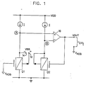
- the improved reference voltage generator includes a pair of reference voltage generating FET devices Q1 and Q2.
- FET devices Q1 and Q2 are identical P-channel enhancement mode FET devices.
- the drain electrodes of FET devices Q1 and Q2 are tied to a common node which is connected to ground potential (GND).
- An operational amplifier 10 has its positive input terminal connected to the source terminal of FET Q1 at node A.
- the negative terminal of operational amplifier 10 is connected to the source electrode of FET device Q2 at node B.
- the output terminal of operational amplifier 10 is connected to the gate or control electrode of FET device Q2.
- the substrate terminal of FET device Q2 is connected to its source terminal.
- a common current source I interconnects the source terminals of FET devices Q1 and Q2 to a single rail power supply (V DD ).
- V BS is the bulk to source voltage formed by the difference between the voltage applied to node 12 and node 14, respectively.
- the voltage at node 12 is positive relative to the voltage on node 14.
- V sub ⁇ V source similarly, the gate or control terminal of Q1 is connected to a control voltage identified as V ACG .
- V ACG and V BS are set by P-channel FET devices with values between V DD and ground. The function of operational amplifier is to keep the voltage at node B equal to the voltage at node A through negative feedback.
- the output of the operational amplifier is the difference between the threshold voltage of Q1 and Q2 having the same polarity and of the same channel implants but having different V BS voltages and thus having different threshold voltages.
- rence ( ⁇ V t ) is determined by the given process. However, it is insensitive to process variation.
- V BS V ACG and constant current (I) for biasing FET devices Q1 and Q2
- V ACG constant current
- I constant current
- Q1′ and Q2′ are the reference voltage setting devices. These devices are similar to Q1 and Q2 of Fig. 1.
- the source electrodes V source of devices Q1′ and Q2′ are connected to node C.
- Node C is connected by devices QS2 and QS1 to single rail power supply V DD .
- Devices QS1 and QS2 are connected in series by their respective drain source terminal at node D.
- each of the devices QS1 and QS2 has its substrate electrode connected to its source electrode and the control gate electrode connected to the drain electrode. It should be noted that by connecting the source and substrate terminal of a device the threshold voltage for that device is substantially the base threshold voltage (V to ).
- P-channel enhancement mode FET device QL is connected between ground potential and the drain terminal of device Q1′.
- P-channel enhancement mode FET device QR is connected between ground potential and the drain terminal of device Q2′.
- Each of the devices QL and QR has its control electrode connected to its drain electrode and its substrate electrode connected to its source electrode. The configuration ensures that the same current is conducted through Q1′ and Q2′.
- Operational amplifier 10′ has its output V out connected to the control electrode of device Q1′.
- the negative input of operational amplifier 10′ is connected at node B′ to the drain terminal of device Q1′.
- width to length ratio (W/L) of device QS1 or QS2 equal to twice the (W/L) ratio of device QR or QL and device Q1′ or Q2′ the current through voltage threshold setting devices Q1′ and Q2′ are identical and the voltage on control terminal 16 is V DD /4.
- the voltage on the substrate terminal (V sub ) of device Q1′ is set by biasing network 18.
- Conductor 20 interconnects the biasing network (at node 22) to V sub .
- Biasing network 18 comprises of a plurality of P-channel enhancement mode devices T1, T2, T3 and T4. The devices are connected in series via their respective source and drain electrodes between V dd and ground potential. Also, the substrate terminal of each device is connected to its source terminal and the control terminal is connected to the drain terminal. If the width/length (W/L) ratios of T1, T2, T3 and T4 are equal, then the value of the voltage at node 22 is V DD /4.
- W represents the width of the device
- L represents the length of the device
- W/L represents the width to length ratio
- the alphanumeric characters identify the particular device.
- V′ out equals (V DD/4 - ⁇ V t ).
- V′ out that is, the reference voltage
- biasing networks that produce voltage level values that are certain percentages of V DD , at node C and node 22, are permissible.
- the biasing networks must be chosen to provide these values.
- Table I lists examples of these values.
- ⁇ represents the fraction of V dd which appears in the output voltage (V out ) as the a.c. ground reference (i.e., 0 ⁇ 1).
- V source represents the percentage of V DD that must be generated at node C.
- V sub represents the percentage of V DD that must be generated at node 22.
- ⁇ V t represents the difference in threshold voltages between Q1′ and Q2′.
- V out is the output voltage. It should be noted that this table is only a representative of preferred values which must be generated at the critical nodes of the circuit in Fig. 2. However, it is within the skill of the art to provide any desired voltage without departing from the spirit and scope of the present invention.
Applications Claiming Priority (2)
| Application Number | Priority Date | Filing Date | Title |
|---|---|---|---|
| US72362 | 1987-07-13 | ||
| US07/072,362 US4837459A (en) | 1987-07-13 | 1987-07-13 | CMOS reference voltage generation |
Publications (2)
| Publication Number | Publication Date |
|---|---|
| EP0301184A1 true EP0301184A1 (fr) | 1989-02-01 |
| EP0301184B1 EP0301184B1 (fr) | 1993-01-13 |
Family
ID=22107093
Family Applications (1)
| Application Number | Title | Priority Date | Filing Date |
|---|---|---|---|
| EP88107309A Expired - Lifetime EP0301184B1 (fr) | 1987-07-13 | 1988-05-06 | Générateur de tension de référence CMOS |
Country Status (4)
| Country | Link |
|---|---|
| US (1) | US4837459A (fr) |
| EP (1) | EP0301184B1 (fr) |
| JP (1) | JPH083767B2 (fr) |
| DE (1) | DE3877451T2 (fr) |
Cited By (5)
| Publication number | Priority date | Publication date | Assignee | Title |
|---|---|---|---|---|
| EP0382929A2 (fr) * | 1989-02-16 | 1990-08-22 | Kabushiki Kaisha Toshiba | Circuit régulateur de tension |
| EP0451870A2 (fr) * | 1990-04-13 | 1991-10-16 | Oki Micro Design Miyazaki Co. Ltd | Circuit de génération d'une tension de référence |
| WO1995006905A1 (fr) * | 1993-08-31 | 1995-03-09 | Tor Sverre Lande | Source de tension de reference analogique programmable par lumiere ultraviolette et utilisee en technologie cmos |
| EP0785494A2 (fr) * | 1991-07-25 | 1997-07-23 | Kabushiki Kaisha Toshiba | Circuit pour génération de tension constante |
| WO1999031801A1 (fr) * | 1997-12-18 | 1999-06-24 | Koninklijke Philips Electronics N.V. | Procede de polarisation d'un circuit integre mos en vue d'une exploitation avec point de coefficient de temperature nul |
Families Citing this family (11)
| Publication number | Priority date | Publication date | Assignee | Title |
|---|---|---|---|---|
| JPH0690655B2 (ja) * | 1987-12-18 | 1994-11-14 | 株式会社東芝 | 中間電位発生回路 |
| US5109187A (en) * | 1990-09-28 | 1992-04-28 | Intel Corporation | CMOS voltage reference |
| JP2544529Y2 (ja) * | 1992-01-31 | 1997-08-20 | 西芝電機株式会社 | ディジタル制御自動電圧調整器の端子電圧検出装置 |
| DE69213213T2 (de) * | 1992-04-16 | 1997-01-23 | Sgs Thomson Microelectronics | Genauer MOS-Schwellenspannungsgenerator |
| SE9400657D0 (sv) * | 1994-02-25 | 1994-02-25 | Ellemtel Utvecklings Ab | En, en kontrollspänning alstrande, krets |
| US5469111A (en) * | 1994-08-24 | 1995-11-21 | National Semiconductor Corporation | Circuit for generating a process variation insensitive reference bias current |
| KR0148732B1 (ko) * | 1995-06-22 | 1998-11-02 | 문정환 | 반도체 소자의 기준전압 발생회로 |
| US7170810B1 (en) | 2005-06-16 | 2007-01-30 | Altera Corporation | Stable programming circuitry for programmable integrated circuits |
| US8487660B2 (en) | 2010-10-19 | 2013-07-16 | Aptus Power Semiconductor | Temperature-stable CMOS voltage reference circuits |
| CN103472883B (zh) | 2012-06-06 | 2015-07-08 | 联咏科技股份有限公司 | 电压产生器及能带隙参考电路 |
| TWI484316B (zh) * | 2012-06-26 | 2015-05-11 | Novatek Microelectronics Corp | 電壓產生器及能帶隙參考電路 |
Citations (3)
| Publication number | Priority date | Publication date | Assignee | Title |
|---|---|---|---|---|
| EP0014149A1 (fr) * | 1979-01-26 | 1980-08-06 | COMMISSARIAT A L'ENERGIE ATOMIQUE Etablissement de Caractère Scientifique Technique et Industriel | Générateur de tension de référence et circuit de mesure de la tension de seuil de transistor MOS, applicable à ce générateur de tension de référence |
| GB2093303A (en) * | 1981-01-20 | 1982-08-25 | Citizen Watch Co Ltd | Voltage sensing circuit |
| US4454467A (en) * | 1981-07-31 | 1984-06-12 | Hitachi, Ltd. | Reference voltage generator |
Family Cites Families (12)
| Publication number | Priority date | Publication date | Assignee | Title |
|---|---|---|---|---|
| US3975648A (en) * | 1975-06-16 | 1976-08-17 | Hewlett-Packard Company | Flat-band voltage reference |
| US4100437A (en) * | 1976-07-29 | 1978-07-11 | Intel Corporation | MOS reference voltage circuit |
| US4472871A (en) * | 1978-09-21 | 1984-09-25 | Mostek Corporation | Method of making a plurality of MOSFETs having different threshold voltages |
| JPS5573114A (en) * | 1978-11-28 | 1980-06-02 | Nippon Gakki Seizo Kk | Output offset control circuit for full step direct-coupled amplifier |
| CH628462A5 (fr) * | 1978-12-22 | 1982-02-26 | Centre Electron Horloger | Source de tension de reference. |
| US4333058A (en) * | 1980-04-28 | 1982-06-01 | Rca Corporation | Operational amplifier employing complementary field-effect transistors |
| DE3173056D1 (en) * | 1980-06-24 | 1986-01-09 | Nec Corp | Linear voltage-current converter |
| US4341963A (en) * | 1980-06-27 | 1982-07-27 | Westinghouse Electric Corp. | Integrated circuit for chip op/amp interface |
| FR2494519A1 (fr) * | 1980-11-14 | 1982-05-21 | Efcis | Generateur de courant integre en technologie cmos |
| US4464588A (en) * | 1982-04-01 | 1984-08-07 | National Semiconductor Corporation | Temperature stable CMOS voltage reference |
| US4453094A (en) * | 1982-06-30 | 1984-06-05 | General Electric Company | Threshold amplifier for IC fabrication using CMOS technology |
| JPS6068414A (ja) * | 1983-09-26 | 1985-04-19 | Hitachi Ltd | 基準電圧発生回路 |
-
1987
- 1987-07-13 US US07/072,362 patent/US4837459A/en not_active Expired - Fee Related
-
1988
- 1988-05-06 DE DE8888107309T patent/DE3877451T2/de not_active Expired - Fee Related
- 1988-05-06 EP EP88107309A patent/EP0301184B1/fr not_active Expired - Lifetime
- 1988-05-19 JP JP63120824A patent/JPH083767B2/ja not_active Expired - Lifetime
Patent Citations (3)
| Publication number | Priority date | Publication date | Assignee | Title |
|---|---|---|---|---|
| EP0014149A1 (fr) * | 1979-01-26 | 1980-08-06 | COMMISSARIAT A L'ENERGIE ATOMIQUE Etablissement de Caractère Scientifique Technique et Industriel | Générateur de tension de référence et circuit de mesure de la tension de seuil de transistor MOS, applicable à ce générateur de tension de référence |
| GB2093303A (en) * | 1981-01-20 | 1982-08-25 | Citizen Watch Co Ltd | Voltage sensing circuit |
| US4454467A (en) * | 1981-07-31 | 1984-06-12 | Hitachi, Ltd. | Reference voltage generator |
Cited By (9)
| Publication number | Priority date | Publication date | Assignee | Title |
|---|---|---|---|---|
| EP0382929A2 (fr) * | 1989-02-16 | 1990-08-22 | Kabushiki Kaisha Toshiba | Circuit régulateur de tension |
| EP0382929A3 (en) * | 1989-02-16 | 1990-09-26 | Kabushiki Kaisha Toshiba | Voltage regulator circuit |
| US5029282A (en) * | 1989-02-16 | 1991-07-02 | Kabushiki Kaisha Toshiba | Voltage regulator circuit |
| EP0451870A2 (fr) * | 1990-04-13 | 1991-10-16 | Oki Micro Design Miyazaki Co. Ltd | Circuit de génération d'une tension de référence |
| EP0451870A3 (en) * | 1990-04-13 | 1992-04-01 | Oki Micro Design Miyazaki Co. Ltd | Reference voltage generating circuit |
| EP0785494A2 (fr) * | 1991-07-25 | 1997-07-23 | Kabushiki Kaisha Toshiba | Circuit pour génération de tension constante |
| EP0785494A3 (fr) * | 1991-07-25 | 1997-08-20 | Toshiba Kk | |
| WO1995006905A1 (fr) * | 1993-08-31 | 1995-03-09 | Tor Sverre Lande | Source de tension de reference analogique programmable par lumiere ultraviolette et utilisee en technologie cmos |
| WO1999031801A1 (fr) * | 1997-12-18 | 1999-06-24 | Koninklijke Philips Electronics N.V. | Procede de polarisation d'un circuit integre mos en vue d'une exploitation avec point de coefficient de temperature nul |
Also Published As
| Publication number | Publication date |
|---|---|
| EP0301184B1 (fr) | 1993-01-13 |
| DE3877451T2 (de) | 1993-07-15 |
| JPS6425220A (en) | 1989-01-27 |
| US4837459A (en) | 1989-06-06 |
| DE3877451D1 (de) | 1993-02-25 |
| JPH083767B2 (ja) | 1996-01-17 |
Similar Documents
| Publication | Publication Date | Title |
|---|---|---|
| EP0301184A1 (fr) | Générateur de tension de référence CMOS | |
| US4742292A (en) | CMOS Precision voltage reference generator | |
| US4839535A (en) | MOS bandgap voltage reference circuit | |
| US5666046A (en) | Reference voltage circuit having a substantially zero temperature coefficient | |
| US4442398A (en) | Integrated circuit generator in CMOS technology | |
| US5517134A (en) | Offset comparator with common mode voltage stability | |
| US5087891A (en) | Current mirror circuit | |
| US4636742A (en) | Constant-current source circuit and differential amplifier using the same | |
| KR100324452B1 (ko) | 조절된캐스코드이득증대를위한궤환증폭기 | |
| KR0134661B1 (ko) | 전위전류 변환기 | |
| US4983929A (en) | Cascode current mirror | |
| KR0126911B1 (ko) | 기준전압 발생회로 및 발생방법 | |
| JPH11353045A (ja) | バンドギャップ型基準電圧発生回路 | |
| EP0305000A2 (fr) | Circuit d'amplificateur comportant un circuit de charge | |
| US5515010A (en) | Dual voltage level shifted, cascoded current mirror | |
| US5045773A (en) | Current source circuit with constant output | |
| US4978868A (en) | Simplified transistor base current compensation circuitry | |
| EP0360887A1 (fr) | Référence de tension CMOS | |
| KR950000432B1 (ko) | 트랜지스터 또는 반도체 장치를 시뮬레이팅할 수 있는 회로 및 포락선 검출기 | |
| US6864741B2 (en) | Low noise resistorless band gap reference | |
| EP0044339B1 (fr) | Circuit miroir de courant | |
| US5495166A (en) | MOS transistor threshold voltage generator | |
| EP0352044B1 (fr) | Circuit de compensation pour le courant de base d'un transistor | |
| EP0290857A1 (fr) | Dispositif de polarisation de grille pour réaliser une capacitance indépendante de la tension | |
| US20050206362A1 (en) | Low-voltage bandgap reference circuit |
Legal Events
| Date | Code | Title | Description |
|---|---|---|---|
| PUAI | Public reference made under article 153(3) epc to a published international application that has entered the european phase |
Free format text: ORIGINAL CODE: 0009012 |
|
| AK | Designated contracting states |
Kind code of ref document: A1 Designated state(s): DE FR GB |
|
| 17P | Request for examination filed |
Effective date: 19890524 |
|
| 17Q | First examination report despatched |
Effective date: 19910122 |
|
| GRAA | (expected) grant |
Free format text: ORIGINAL CODE: 0009210 |
|
| AK | Designated contracting states |
Kind code of ref document: B1 Designated state(s): DE FR GB |
|
| REF | Corresponds to: |
Ref document number: 3877451 Country of ref document: DE Date of ref document: 19930225 |
|
| ET | Fr: translation filed | ||
| PLBE | No opposition filed within time limit |
Free format text: ORIGINAL CODE: 0009261 |
|
| STAA | Information on the status of an ep patent application or granted ep patent |
Free format text: STATUS: NO OPPOSITION FILED WITHIN TIME LIMIT |
|
| 26N | No opposition filed | ||
| PGFP | Annual fee paid to national office [announced via postgrant information from national office to epo] |
Ref country code: FR Payment date: 19960507 Year of fee payment: 9 |
|
| PGFP | Annual fee paid to national office [announced via postgrant information from national office to epo] |
Ref country code: GB Payment date: 19970422 Year of fee payment: 10 |
|
| PGFP | Annual fee paid to national office [announced via postgrant information from national office to epo] |
Ref country code: DE Payment date: 19970521 Year of fee payment: 10 |
|
| PG25 | Lapsed in a contracting state [announced via postgrant information from national office to epo] |
Ref country code: FR Free format text: LAPSE BECAUSE OF NON-PAYMENT OF DUE FEES Effective date: 19980130 |
|
| REG | Reference to a national code |
Ref country code: FR Ref legal event code: ST |
|
| PG25 | Lapsed in a contracting state [announced via postgrant information from national office to epo] |
Ref country code: GB Free format text: LAPSE BECAUSE OF NON-PAYMENT OF DUE FEES Effective date: 19980506 |
|
| GBPC | Gb: european patent ceased through non-payment of renewal fee |
Effective date: 19980506 |
|
| PG25 | Lapsed in a contracting state [announced via postgrant information from national office to epo] |
Ref country code: DE Free format text: LAPSE BECAUSE OF NON-PAYMENT OF DUE FEES Effective date: 19990302 |