EP0300524A1 - Dispositif d'atténuation variable destiné à être inséré entre un circuit émetteur et un circuit de charge - Google Patents
Dispositif d'atténuation variable destiné à être inséré entre un circuit émetteur et un circuit de charge Download PDFInfo
- Publication number
- EP0300524A1 EP0300524A1 EP88201248A EP88201248A EP0300524A1 EP 0300524 A1 EP0300524 A1 EP 0300524A1 EP 88201248 A EP88201248 A EP 88201248A EP 88201248 A EP88201248 A EP 88201248A EP 0300524 A1 EP0300524 A1 EP 0300524A1
- Authority
- EP
- European Patent Office
- Prior art keywords
- circuit
- attenuation
- variable
- diodes
- parallel
- Prior art date
- Legal status (The legal status is an assumption and is not a legal conclusion. Google has not performed a legal analysis and makes no representation as to the accuracy of the status listed.)
- Granted
Links
Images
Classifications
-
- H—ELECTRICITY
- H03—ELECTRONIC CIRCUITRY
- H03H—IMPEDANCE NETWORKS, e.g. RESONANT CIRCUITS; RESONATORS
- H03H7/00—Multiple-port networks comprising only passive electrical elements as network components
- H03H7/24—Frequency- independent attenuators
- H03H7/25—Frequency- independent attenuators comprising an element controlled by an electric or magnetic variable
- H03H7/253—Frequency- independent attenuators comprising an element controlled by an electric or magnetic variable the element being a diode
- H03H7/255—Frequency- independent attenuators comprising an element controlled by an electric or magnetic variable the element being a diode the element being a PIN diode
Definitions
- the present invention relates to a variable attenuation device intended to be inserted between a transmitter circuit having a certain internal impedance and a load circuit, device formed by at least one parallel attenuation branch formed from a resistance element.
- variable PIN diode
- a bias circuit to vary the resistance of the element as a function of an attenuation control quantity.
- Such devices are well known and find important applications in particular as an amplitude modulator of a radio transmitter, the modulation acting as an attenuation control quantity. Efforts are made in this type of application, in order to obtain good modulation dynamics, to be able to withstand relatively high powers of the transmitter circuit.
- the object of the present invention is to provide an attenuation device capable of withstanding high power.
- the parallel attenuation branch comprises a dissipative element which is placed in series with the variable resistance element and whose value ensures the adaptation of the internal impedance of the transmitter circuit.
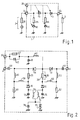
- Figure 1 shows the block diagram of the attenuation device according to the invention.
- FIG. 2 represents the diagram of the preferred embodiment of the attenuation device according to the invention.
- the reference 1 indicates the attenuation device to be inserted between an emitter circuit 2 which is connected between the input terminal 4 and the earth and a load circuit 5 which is connected between the output terminal 6 and the earth.
- the device is made up of P.I.N. 10, 11, 12 and 13 placed either in parallel (diodes 10 and 12), or in series (diodes 11 and 13).
- a bias circuit has been provided, shown simply in dotted lines in this FIG. 1, which allows the PIN diodes to be suitably biased from a control voltage applied to the control terminal. 20.
- resistive elements 25 and 26 have been arranged in series with the diodes 10 and 12 and the value of the resistance of these elements is such that it ensures both the adaptation of the internal resistance of the emitter circuit 2 , represented by the reference 30, than that of the charging circuit 5.
- FIG. 2 shows the embodiment of the device and details the diode bias circuit 10, 11, 12, 13 well.
- the references representing the elements already described in FIG. 1 remain unchanged.
- a first isolation capacitor 40 has been arranged between terminal 4 and the cathode of the diode 11 and a second isolation capacitor. 41 between terminal 6 and the cathode of diode 13.
- the anodes of diodes 11 and 13 are connected to terminal 20 by means of a blocking inductor 42 and an RC circuit formed by a resistor 43 and a capacitor 45 in parallel.
- a capacitor 48 connects the common point of the choke 42 and the RC circuit to ground.
- the anodes of diodes 11 and 13 are connected to ground for direct current via element 26, by a choke 50 and a resistor 52.
- the cathode of diode 13 is connected to ground via of a choke 55 and of the aforementioned resistor 52.
- the cathode of the diode 11 is connected to the earth always with regard to the direct current by means of a first circuit formed of the element 25, of a inductor 58 and a resistor 60 and a second circuit formed by an inductor 62 and the aforementioned resistor 60.
- the anodes of diodes 10 and 12 receive a DC voltage from a voltage generator 69 and via inductors 70 and 72 respectively.
- Capacitors 73 and 75 connected between the anodes of diodes 10 and 12 provide a path to earth for high frequency currents. It is also possible to provide for the connection of a capacitor 78 in parallel on the generator 69.
- the applicant has noticed that by connecting a capacitor 80 of relatively low capacity across the terminals of element 26, the adaptation of the device.
- the generator 69 supplies, in the absence of control voltage to terminal 20, a voltage such that the diodes 10 and 12 are in the on state and the diodes 11 and 13 in the state blocked; the attenuation is then maximum, the emitter circuit 2 is looped by the element 25 whose value corresponds to its internal resistance.
- the diodes 11 and 13 start to drive and the diodes 10 and 12 are less busy.
- the diodes 11 and 13 are completely on and the diodes 10 and 12 completely blocked, the attenuation is minimal.
- the R.O.S. (standing wave ratio) remains less than 1.6 for an attenuation varying from less than 2 dB to more than 50 dB - the power at the input being several watts - modulation frequencies ranging from 0 to 25 kHz with a voltage at terminal 20 ranging from 0 to 10 Volts.
- the attenuation is not a linear function of the voltage applied to the control terminal 20 and it is up to the user to provide, before terminal 20, any non-linear circuit which will give it the characteristic d desired attenuation.
Abstract
Description
- La présente invention concerne un dispositif d'atténuation variable destiné à être inséré entre un circuit émetteur présentant une certaine impédance interne et un circuit de charge, dispositif formé d'au moins une branche d'atténuation parallèle constituée à partir d'un élément à résistance variable (diode PIN) et d'un circuit de polarisation pour faire varier la résistance de l'élément en fonction d'une grandeur de commande d'atténuation.
- De tels dispositifs sont bien connus et trouvent d'importantes applications notamment comme modulateur d'amplitude d'un émetteur radio, la modulation agissant comme grandeur de commande d'atténuation. On s'efforce dans ce genre d'application, afin d'obtenir une bonne dynamique de modulation, de pouvoir supporter des puissances relativement élevées du circuit émetteur.
- Les dispositifs d'atténuation connus, par exemple celui décrit dans le brevet des ETATS-UNIS D'AMERIQUE No 4 009 456, ne conviennent pas pour supporter des puissances importantes.
- La présente invention a pour but de fournir un dispositif d'atténuation capable de supporter une puissance élevée.
- Pour cela, un tel dispositif est remarquable en ce que la branche d'atténuation parallèle comporte un élément dissipatif qui est placé en série avec l'élément à résistance variable et dont la valeur assure l'adaptation de l'impédance interne du circuit émetteur.
- Dans l'application envisagée, pour obtenir de bonnes performances en tant que modulateur, la demanderesse s'est rendue compte que le choix de diodes P.I.N. est capital. Selon une caractéristique importante de l'invention, les éléments à résistances variables sont des diodes P.I.N. présentant des durées de vie de porteurs minoritaires comprises entre 3 et 5 µs et une pente de la caractéristique Rs/If présentant une valeur entre 35 et 80 Ω pour un courant If = 1 mA et une valeur supérieure à 350 Ω pour If = 300 µA.
- Rs représente la valeur de la résistance et If le courant traversant la diode P.I.N.
- La description suivante, accompagnée des dessins annexés, le tout donné à titre d'exemple non limitatif fera bien comprendre comment l'invention peut être réalisée.
- La figure 1 représente le schéma de principe du dispositif d'atténuation conforme à l'invention.
- La figure 2 représente le schéma du mode de réalisation préféré du dispositif d'atténuation conforme à l'invention.
- A la figure 1, la reférence 1 indique le dispositif d'atténuation à insérer entre un circuit émetteur 2 qui vient se connecter entre la borne d'entrée 4 et la terre et un circuit de charge 5 qui se connecte entre la borne de sortie 6 et la terre. Le dispositif est constitué à partir de diodes P.I.N. 10, 11, 12 et 13 placées soit en parallèle (diodes 10 et 12), soit en série (diodes 11 et 13). Pour faire varier la conduction de ces diodes, on a prévu un circuit de polarisation, montré simplement en pointillé à cette figure 1, qui permet de polariser les diodes PIN de façon convenable à partir d'une tension de commande appliquée à la borne de commande 20.
- Conformément à l'invention, on a disposé des éléments résistifs 25 et 26 en série avec les diodes 10 et 12 et la valeur de la résistance de ces éléments est telle qu'elle assure tant l'adaptation de la résistance interne du circuit émetteur 2, représentée par la référence 30, que celle du circuit de charge 5.
- La figure 2 montre le schéma de réalisation du dispositif et détaille bien le circuit de polarisation des diodes 10, 11, 12, 13. Les références représentant les éléments déjà décrits à la figure 1 restent inchangées. De façon à pouvoir isoler du point de vue courant continu le dispositif des circuits émetteurs et du circuit de charge, on a disposé un premier condensateur d'isolement 40 entre la borne 4 et la cathode de la diode 11 et un deuxième condensateur d'isolement 41 entre la borne 6 et la cathode de la diode 13. Les anodes des diodes 11 et 13 sont reliées à la borne 20 par l'intermédiaire d'une self de blocage 42 et un circuit RC formé d'une résistance 43 et d'un condensateur 45 en parallèle. Un condensateur 48 réunit à la masse le point commun de la self 42 et du circuit RC. Les anodes des diodes 11 et 13 sont réunies à la masse pour le courant continu par l'intermédiaire de l'élément 26, par une self 50 et une résistance 52. La cathode de la diode 13 est reliée à la masse par l'intermédiaire d'une self 55 et de la résistance précitée 52. La cathode de la diode 11 est reliée à la terre toujours en ce qui concerne le courant continu par l'intermédiaire d'un premier circuit formé de l'élément 25, d'une self 58 et d'une résistance 60 et d'un deuxième circuit formé d'une self 62 et la résistance précitée 60.
- Les anodes des diodes 10 et 12 reçoivent une tension continue provenant d'un générateur de tension 69 et par l'intermédiaire de selfs 70 et 72 respectivement. Des condensateurs 73 et 75 branchés entre les anodes des diodes 10 et 12 assurent un chemin vers la terre pour les courants à haute fréquence. On peut aussi prévoir le branchement d'un condensateur 78 en parallèle sur le générateur 69. En outre, la demanderesse s'est aperçu qu'en connectant un condensateur 80 de capacité relativement faible aux bornes de l'élément 26, on améliore l'adaptation du dispositif.
- Le générateur 69 fournit, en l'absence de tension de commande à la borne 20, une tension telle que les diodes 10 et 12 sont à l'état passant et les diodes 11 et 13 à l'état bloqué ; l'atténuation est alors maximum, le circuit émetteur 2 est bouclé par l'élément 25 dont la valeur correspond à sa résistance interne.
- Lorsque à la borne 20 la tension croît, les diodes 11 et 13 commencent à conduire et les diodes 10 et 12 sont moins passantes. Lorsque les diodes 11 et 13 sont totalement passantes et les diodes 10 et 12 complètement bloquées, l'atténuation est minimale.
- La demanderesse a trouvé que les valeurs des éléments données au Tableau ci-dessous procurent de meilleurs résultats dans la gamme de fréquences allant de 100 MHz à 400 MHz.

- Hormis ces paramètres d'atténuation et de dissipation, les caractéristiques des diodes PIN ont un rôle capital, notamment en ce qui concerne la distorsion de modulation et la réjection harmonique. Dans ces conditions particulières d'utilisation, deux paramètres sont prépondérants :
- a) la durée de vie des porteurs minoritaires : celle-ci doit être comprise entre 3 et 5 µs.
- b) la pente de la caractéristique Rs/If. Elle peut être définie par la valeur de la résistance "série" en deux points de la caractéristique : celle-ci doit être comprise entre 35 Ω et 80 Ω pour IF = 1 mA, et supérieure à 350 Ω pour IF = 100 µA.
- Avec de telles valeurs et circuits émetteurs présentant une résistance interne de 50 Ω égale à celle du circuit de charge, le R.O.S. (rapport d'onde stationnaire) reste inférieur à 1,6 pour une atténuation variant de moins de 2 dB à plus de 50 dB -la puissance à l'entrée étant de plusieurs watts- les fréquences de modulation allant de 0 à 25 kHz avec une tension à la borne 20 allant de 0 à 10 Volts.
- Il doit être signalé que l'atténuation n'est pas une fonction linéaire de la tension appliquée à la borne de commande 20 et il appartient à l'utilisateur de prévoir, avant la borne 20, tout circuit non linéaire qui lui procurera la caractéristique d'atténuation désirée.
DH 493-19 fabriquée par THOMSON-CSF en FRANCE
et DSB6479-42 fabriquée par ALPHA INDUSTRIES aux ETATS-UNIS
conviennent pour le dispositif conforme à l'invention.
Claims (3)
Applications Claiming Priority (2)
| Application Number | Priority Date | Filing Date | Title |
|---|---|---|---|
| FR8709208A FR2617655B1 (fr) | 1987-06-30 | 1987-06-30 | Dispositif d'attenuation variable destine a etre insere entre un circuit emetteur et un circuit de charge |
| FR8709208 | 1987-06-30 |
Publications (2)
| Publication Number | Publication Date |
|---|---|
| EP0300524A1 true EP0300524A1 (fr) | 1989-01-25 |
| EP0300524B1 EP0300524B1 (fr) | 1993-09-08 |
Family
ID=9352676
Family Applications (1)
| Application Number | Title | Priority Date | Filing Date |
|---|---|---|---|
| EP88201248A Expired - Lifetime EP0300524B1 (fr) | 1987-06-30 | 1988-06-17 | Dispositif d'atténuation variable destiné à être inséré entre un circuit émetteur et un circuit de charge |
Country Status (5)
| Country | Link |
|---|---|
| US (1) | US4942375A (fr) |
| EP (1) | EP0300524B1 (fr) |
| JP (1) | JPS6432713A (fr) |
| DE (1) | DE3883883T2 (fr) |
| FR (1) | FR2617655B1 (fr) |
Cited By (2)
| Publication number | Priority date | Publication date | Assignee | Title |
|---|---|---|---|---|
| FR2676150A1 (fr) * | 1991-05-03 | 1992-11-06 | Thomson Csf | Circuit attenuateur limiteur commandable a diode a zone intermediaire asga et utilisation d'un tel circuit. |
| US6362704B1 (en) | 1998-10-07 | 2002-03-26 | Nokia Corporation | Circuit arrangement improving the control characteristics of an attenuator |
Families Citing this family (14)
| Publication number | Priority date | Publication date | Assignee | Title |
|---|---|---|---|---|
| JPH0475423U (fr) * | 1990-11-14 | 1992-07-01 | ||
| US5332981A (en) * | 1992-07-31 | 1994-07-26 | Emc Technology, Inc. | Temperature variable attenuator |
| US5345123A (en) * | 1993-07-07 | 1994-09-06 | Motorola, Inc. | Attenuator circuit operating with single point control |
| JP3063513B2 (ja) * | 1994-02-10 | 2000-07-12 | 松下電器産業株式会社 | マイクロ波検波給電回路 |
| SE508506C2 (sv) * | 1997-02-25 | 1998-10-12 | Ericsson Telefon Ab L M | Anordning och förfarande vid telekommunikation |
| US6144265A (en) * | 1997-11-26 | 2000-11-07 | Honeywell Inc. | Calibrated high power radio frequency step attenuator |
| US5969561A (en) * | 1998-03-05 | 1999-10-19 | Diablo Research Company, Llc | Integrated circuit having a variable RF resistor |
| KR20000045594A (ko) * | 1998-12-30 | 2000-07-25 | 김영환 | 초단파 및 극초단파 대역용 소형 가변 감쇠기 |
| US6919774B2 (en) * | 2001-10-03 | 2005-07-19 | Microtune (Texas), L.P. | Broadband PIN diode attenuator bias network |
| DE10234479A1 (de) * | 2002-07-29 | 2004-02-12 | Infineon Technologies Ag | Übertragungssystem |
| US8212648B2 (en) * | 2004-10-13 | 2012-07-03 | Yantel Corporation | Variable attenuator |
| WO2010095295A1 (fr) | 2009-02-20 | 2010-08-26 | 株式会社村田製作所 | Element de memoire resistive et utilisation associee |
| JP5459516B2 (ja) | 2009-02-20 | 2014-04-02 | 株式会社村田製作所 | 抵抗記憶素子およびその使用方法 |
| US8903344B2 (en) * | 2010-11-30 | 2014-12-02 | Qualcomm Incorporated | Programmable attenuator |
Citations (3)
| Publication number | Priority date | Publication date | Assignee | Title |
|---|---|---|---|---|
| DE2912434A1 (de) * | 1979-03-29 | 1980-10-09 | Bosch Gmbh Robert | Vorrichtung zur amplitudenregelung hochfrequenter signale |
| US4378536A (en) * | 1981-06-09 | 1983-03-29 | Rca Corporation | High power, low frequency, electronically adjustable attenuator |
| US4621244A (en) * | 1984-05-17 | 1986-11-04 | At&T Bell Laboratories | Broadband variable attenuator using transmission lines series coupled by adjustable pin diodes |
Family Cites Families (16)
| Publication number | Priority date | Publication date | Assignee | Title |
|---|---|---|---|---|
| US3529266A (en) * | 1968-08-12 | 1970-09-15 | Us Army | Continuously and dynamically variable pin diode attenuator |
| US3846724A (en) * | 1973-07-25 | 1974-11-05 | Saba Gmbh | Adjustable attenuator with p-i-n diodes |
| NL7506265A (nl) * | 1975-05-28 | 1976-11-30 | Philips Nv | Regelbare hf-signaalverzwakker. |
| US4097827A (en) * | 1977-02-04 | 1978-06-27 | The United States Of America As Represented By The Secretary Of The Air Force | Constant impedance, constant phase pin diode with attenuator |
| US4216445A (en) * | 1978-12-22 | 1980-08-05 | The United States Of America As Represented By The Secretary Of The Army | Variable resistance attenuator |
| US4236126A (en) * | 1979-04-25 | 1980-11-25 | Cincinnati Electronics Corporation | Variable RF attenuator |
| SU866618A1 (ru) * | 1980-01-18 | 1981-09-23 | Предприятие П/Я В-2640 | Электрически управл емый аттенюатор |
| JPS5744314A (en) * | 1980-08-29 | 1982-03-12 | Nec Corp | Variable attenuator |
| JPS59216311A (ja) * | 1983-05-24 | 1984-12-06 | Matsushita Electric Ind Co Ltd | 可変抵抗減衰器 |
| JPS60160716A (ja) * | 1984-02-01 | 1985-08-22 | Nec Corp | 電圧制御減衰器 |
| JPS60260220A (ja) * | 1984-06-06 | 1985-12-23 | Sharp Corp | Rf可変減衰回路 |
| JPH0247127B2 (ja) * | 1984-06-13 | 1990-10-18 | Nippon Electric Co | Daioodogensuiki |
| JPS6173054A (ja) * | 1984-09-17 | 1986-04-15 | メデイカル テクノロジ− コ−ポレ−シヨン | 試料調整用小瓶 |
| SU1293773A1 (ru) * | 1985-04-01 | 1987-02-28 | Предприятие П/Я В-8150 | Электрически управл емый аттенюатор |
| JPH0672837B2 (ja) * | 1985-12-25 | 1994-09-14 | アンドレアス・スツアバドス | ペースト状試料物質用の検査容器 |
| JPS62200809A (ja) * | 1986-02-28 | 1987-09-04 | Fujitsu Ltd | 電圧制御形可変減衰器 |
-
1987
- 1987-06-30 FR FR8709208A patent/FR2617655B1/fr not_active Expired - Fee Related
-
1988
- 1988-06-17 EP EP88201248A patent/EP0300524B1/fr not_active Expired - Lifetime
- 1988-06-17 DE DE88201248T patent/DE3883883T2/de not_active Expired - Fee Related
- 1988-06-28 JP JP63158210A patent/JPS6432713A/ja active Pending
-
1989
- 1989-09-15 US US07/408,455 patent/US4942375A/en not_active Expired - Fee Related
Patent Citations (3)
| Publication number | Priority date | Publication date | Assignee | Title |
|---|---|---|---|---|
| DE2912434A1 (de) * | 1979-03-29 | 1980-10-09 | Bosch Gmbh Robert | Vorrichtung zur amplitudenregelung hochfrequenter signale |
| US4378536A (en) * | 1981-06-09 | 1983-03-29 | Rca Corporation | High power, low frequency, electronically adjustable attenuator |
| US4621244A (en) * | 1984-05-17 | 1986-11-04 | At&T Bell Laboratories | Broadband variable attenuator using transmission lines series coupled by adjustable pin diodes |
Non-Patent Citations (1)
| Title |
|---|
| ELECTRONIC DESIGN, vol. 25, no. 7, 29 mars 1977, pages 100-102, Rochelle Park, US; R.S. VILES: "Need a PIN-diode attenuator" * |
Cited By (2)
| Publication number | Priority date | Publication date | Assignee | Title |
|---|---|---|---|---|
| FR2676150A1 (fr) * | 1991-05-03 | 1992-11-06 | Thomson Csf | Circuit attenuateur limiteur commandable a diode a zone intermediaire asga et utilisation d'un tel circuit. |
| US6362704B1 (en) | 1998-10-07 | 2002-03-26 | Nokia Corporation | Circuit arrangement improving the control characteristics of an attenuator |
Also Published As
| Publication number | Publication date |
|---|---|
| DE3883883T2 (de) | 1994-04-14 |
| US4942375A (en) | 1990-07-17 |
| FR2617655B1 (fr) | 1994-05-20 |
| FR2617655A1 (fr) | 1989-01-06 |
| EP0300524B1 (fr) | 1993-09-08 |
| DE3883883D1 (de) | 1993-10-14 |
| JPS6432713A (en) | 1989-02-02 |
Similar Documents
| Publication | Publication Date | Title |
|---|---|---|
| EP0300524B1 (fr) | Dispositif d'atténuation variable destiné à être inséré entre un circuit émetteur et un circuit de charge | |
| EP0348283A1 (fr) | Multiplicateur de fréquence à rang de multiplication programmable | |
| EP0660512A1 (fr) | Amplificateur déphaseur et son application à un circuit recombineur | |
| EP0720292A1 (fr) | Dispositif terminal mobile pour télécommunication incluant un circuit commutateur | |
| EP0612141A2 (fr) | Procédé et dispositif de commande de puissance pour un circuit comportant un onduleur à résonance | |
| EP0377205B1 (fr) | Limiteur en courant et récepteur optique en faisant application | |
| FR2737065A1 (fr) | Dispositif semiconducteur incluant un amplificateur de puissance et appareil de telecommunication mobile incluant un tel dispositif semiconducteur | |
| FR2460576A1 (fr) | Circuit d'alimentation a trois bornes pour appareil telephonique | |
| FR2538193A1 (fr) | Interface de sortie pour circuit logique a trois etats dans un circuit integre a transistors mos | |
| EP0277855B1 (fr) | Convertisseur binaire-bipolaire | |
| EP0301635B1 (fr) | Dispositif interrupteur pour signaux à haute fréquence | |
| EP0203663B1 (fr) | Oscillateur hyperfréquence de puissance, modulé linéairement sur une grande plage de fréquence | |
| EP0120756B1 (fr) | Oscillateur comprenant un amplificateur passe-bande haute-fréquence à impédance adaptable | |
| FR2581275A1 (fr) | Recepteur de signaux optiques a tres large bande. | |
| EP0708525B1 (fr) | Etage amplificateur de puissance délivrant un signal rectangulaire d'amplitude controlée | |
| EP0119927B1 (fr) | Amplificateur haute tension pour charge capacitive | |
| EP0362583B1 (fr) | Modulateur hyperfréquence à deux états de phase: O, Pi à très faibles pertes | |
| EP0046421B1 (fr) | Récepteur pour système de transmission de signaux par rayonnement électromagnétique, notamment infrarouge | |
| EP1047132A1 (fr) | Dispositif de circuit intégré comprenant une inductance à haut coefficient de qualité | |
| EP0103520B1 (fr) | Circuit d'entrée et d'alimentation pour filtre, notamment un filtre de récepteur de télécommande centralisée | |
| FR2532799A1 (fr) | Filtre passe-haut a condensateur commute | |
| EP0021909A1 (fr) | Oscillateur pour hyperfréquences, stabilisé, à conversion de fréquence, et sa réalisation à l'état solide | |
| WO2023144200A1 (fr) | Amplificateur audio haute performance | |
| FR2605816A1 (fr) | Oscillateur hyperfrequence a transistor, accordable par tension et generateur hyperfrequence a large bande comportant de tels oscillateurs | |
| CH631034A5 (en) | Modulation circuit |
Legal Events
| Date | Code | Title | Description |
|---|---|---|---|
| PUAI | Public reference made under article 153(3) epc to a published international application that has entered the european phase |
Free format text: ORIGINAL CODE: 0009012 |
|
| AK | Designated contracting states |
Kind code of ref document: A1 Designated state(s): DE FR GB IT SE |
|
| 17P | Request for examination filed |
Effective date: 19890713 |
|
| 17Q | First examination report despatched |
Effective date: 19910812 |
|
| ITTA | It: last paid annual fee | ||
| GRAA | (expected) grant |
Free format text: ORIGINAL CODE: 0009210 |
|
| AK | Designated contracting states |
Kind code of ref document: B1 Designated state(s): DE FR GB IT SE |
|
| REF | Corresponds to: |
Ref document number: 3883883 Country of ref document: DE Date of ref document: 19931014 |
|
| ITF | It: translation for a ep patent filed |
Owner name: ING. C. GREGORJ S.P.A. |
|
| GBT | Gb: translation of ep patent filed (gb section 77(6)(a)/1977) |
Effective date: 19931207 |
|
| PLBE | No opposition filed within time limit |
Free format text: ORIGINAL CODE: 0009261 |
|
| STAA | Information on the status of an ep patent application or granted ep patent |
Free format text: STATUS: NO OPPOSITION FILED WITHIN TIME LIMIT |
|
| 26N | No opposition filed | ||
| EAL | Se: european patent in force in sweden |
Ref document number: 88201248.7 |
|
| ITPR | It: changes in ownership of a european patent |
Owner name: CAMBIO RAGIONE SOCIALE;PHILIPS ELECTRONICS N.V. |
|
| PGFP | Annual fee paid to national office [announced via postgrant information from national office to epo] |
Ref country code: FR Payment date: 19970620 Year of fee payment: 10 |
|
| PGFP | Annual fee paid to national office [announced via postgrant information from national office to epo] |
Ref country code: GB Payment date: 19980601 Year of fee payment: 11 |
|
| PGFP | Annual fee paid to national office [announced via postgrant information from national office to epo] |
Ref country code: SE Payment date: 19980625 Year of fee payment: 11 |
|
| PGFP | Annual fee paid to national office [announced via postgrant information from national office to epo] |
Ref country code: DE Payment date: 19980824 Year of fee payment: 11 |
|
| PG25 | Lapsed in a contracting state [announced via postgrant information from national office to epo] |
Ref country code: FR Free format text: LAPSE BECAUSE OF NON-PAYMENT OF DUE FEES Effective date: 19990226 |
|
| REG | Reference to a national code |
Ref country code: FR Ref legal event code: ST |
|
| PG25 | Lapsed in a contracting state [announced via postgrant information from national office to epo] |
Ref country code: GB Free format text: LAPSE BECAUSE OF NON-PAYMENT OF DUE FEES Effective date: 19990617 |
|
| PG25 | Lapsed in a contracting state [announced via postgrant information from national office to epo] |
Ref country code: SE Free format text: THE PATENT HAS BEEN ANNULLED BY A DECISION OF A NATIONAL AUTHORITY Effective date: 19990629 |
|
| GBPC | Gb: european patent ceased through non-payment of renewal fee |
Effective date: 19990617 |
|
| EUG | Se: european patent has lapsed |
Ref document number: 88201248.7 |
|
| PG25 | Lapsed in a contracting state [announced via postgrant information from national office to epo] |
Ref country code: DE Free format text: LAPSE BECAUSE OF NON-PAYMENT OF DUE FEES Effective date: 20000503 |
|
| PG25 | Lapsed in a contracting state [announced via postgrant information from national office to epo] |
Ref country code: IT Free format text: LAPSE BECAUSE OF NON-PAYMENT OF DUE FEES;WARNING: LAPSES OF ITALIAN PATENTS WITH EFFECTIVE DATE BEFORE 2007 MAY HAVE OCCURRED AT ANY TIME BEFORE 2007. THE CORRECT EFFECTIVE DATE MAY BE DIFFERENT FROM THE ONE RECORDED. Effective date: 20050617 |