EP0289196A2 - High frequency resonant power converter - Google Patents
High frequency resonant power converter Download PDFInfo
- Publication number
- EP0289196A2 EP0289196A2 EP88303521A EP88303521A EP0289196A2 EP 0289196 A2 EP0289196 A2 EP 0289196A2 EP 88303521 A EP88303521 A EP 88303521A EP 88303521 A EP88303521 A EP 88303521A EP 0289196 A2 EP0289196 A2 EP 0289196A2
- Authority
- EP
- European Patent Office
- Prior art keywords
- switch
- resonant
- power converter
- circuit
- primary winding
- Prior art date
- Legal status (The legal status is an assumption and is not a legal conclusion. Google has not performed a legal analysis and makes no representation as to the accuracy of the status listed.)
- Withdrawn
Links
Images


Classifications
-
- H—ELECTRICITY
- H02—GENERATION; CONVERSION OR DISTRIBUTION OF ELECTRIC POWER
- H02M—APPARATUS FOR CONVERSION BETWEEN AC AND AC, BETWEEN AC AND DC, OR BETWEEN DC AND DC, AND FOR USE WITH MAINS OR SIMILAR POWER SUPPLY SYSTEMS; CONVERSION OF DC OR AC INPUT POWER INTO SURGE OUTPUT POWER; CONTROL OR REGULATION THEREOF
- H02M1/00—Details of apparatus for conversion
- H02M1/42—Circuits or arrangements for compensating for or adjusting power factor in converters or inverters
-
- H—ELECTRICITY
- H02—GENERATION; CONVERSION OR DISTRIBUTION OF ELECTRIC POWER
- H02M—APPARATUS FOR CONVERSION BETWEEN AC AND AC, BETWEEN AC AND DC, OR BETWEEN DC AND DC, AND FOR USE WITH MAINS OR SIMILAR POWER SUPPLY SYSTEMS; CONVERSION OF DC OR AC INPUT POWER INTO SURGE OUTPUT POWER; CONTROL OR REGULATION THEREOF
- H02M1/00—Details of apparatus for conversion
- H02M1/44—Circuits or arrangements for compensating for electromagnetic interference in converters or inverters
-
- H—ELECTRICITY
- H02—GENERATION; CONVERSION OR DISTRIBUTION OF ELECTRIC POWER
- H02M—APPARATUS FOR CONVERSION BETWEEN AC AND AC, BETWEEN AC AND DC, OR BETWEEN DC AND DC, AND FOR USE WITH MAINS OR SIMILAR POWER SUPPLY SYSTEMS; CONVERSION OF DC OR AC INPUT POWER INTO SURGE OUTPUT POWER; CONTROL OR REGULATION THEREOF
- H02M3/00—Conversion of dc power input into dc power output
- H02M3/22—Conversion of dc power input into dc power output with intermediate conversion into ac
- H02M3/24—Conversion of dc power input into dc power output with intermediate conversion into ac by static converters
- H02M3/28—Conversion of dc power input into dc power output with intermediate conversion into ac by static converters using discharge tubes with control electrode or semiconductor devices with control electrode to produce the intermediate ac
- H02M3/325—Conversion of dc power input into dc power output with intermediate conversion into ac by static converters using discharge tubes with control electrode or semiconductor devices with control electrode to produce the intermediate ac using devices of a triode or a transistor type requiring continuous application of a control signal
- H02M3/335—Conversion of dc power input into dc power output with intermediate conversion into ac by static converters using discharge tubes with control electrode or semiconductor devices with control electrode to produce the intermediate ac using devices of a triode or a transistor type requiring continuous application of a control signal using semiconductor devices only
- H02M3/337—Conversion of dc power input into dc power output with intermediate conversion into ac by static converters using discharge tubes with control electrode or semiconductor devices with control electrode to produce the intermediate ac using devices of a triode or a transistor type requiring continuous application of a control signal using semiconductor devices only in push-pull configuration
- H02M3/3376—Conversion of dc power input into dc power output with intermediate conversion into ac by static converters using discharge tubes with control electrode or semiconductor devices with control electrode to produce the intermediate ac using devices of a triode or a transistor type requiring continuous application of a control signal using semiconductor devices only in push-pull configuration with automatic control of output voltage or current
-
- Y—GENERAL TAGGING OF NEW TECHNOLOGICAL DEVELOPMENTS; GENERAL TAGGING OF CROSS-SECTIONAL TECHNOLOGIES SPANNING OVER SEVERAL SECTIONS OF THE IPC; TECHNICAL SUBJECTS COVERED BY FORMER USPC CROSS-REFERENCE ART COLLECTIONS [XRACs] AND DIGESTS
- Y02—TECHNOLOGIES OR APPLICATIONS FOR MITIGATION OR ADAPTATION AGAINST CLIMATE CHANGE
- Y02B—CLIMATE CHANGE MITIGATION TECHNOLOGIES RELATED TO BUILDINGS, e.g. HOUSING, HOUSE APPLIANCES OR RELATED END-USER APPLICATIONS
- Y02B70/00—Technologies for an efficient end-user side electric power management and consumption
- Y02B70/10—Technologies improving the efficiency by using switched-mode power supplies [SMPS], i.e. efficient power electronics conversion e.g. power factor correction or reduction of losses in power supplies or efficient standby modes
Definitions
- a common disadvantage of many types of existing power converters with single mode resonant power throughput is the disproportionate voltage and current stress placed on the power train components relative to the level of power throughput.
- Further disadvantages of existing resonant power converters include limitation to a single switching device i.e. single ended converters) and limitations on the duty cycle range of the power switch. These single ended converters have a unidirectional flux excursion in the power transformer and hence need the added complexity of a core reset circuit.
- One such single ended resonant zero current switching power converter having a unidirectional flux excursion in the power transformer is disclosed in U.S. patent 4,415,959. It therefore requires a commutation switch in order to reset the transformer core and to provide continuous power to the load.
- the current flowing through transistor 14 has a sinusoidal wave form and continues conducting in duration sufficiently to complete a full half cycle current waveform for which eventually terminates at t3. This is shown in current waveform in FIG. 4, part A which extends from t0 to t3.
- a current shown by waveform 470 in FIG. 4, part 6 is flowing through the rectifying diode 35 and at the time t0 has a value equal to 1/2 the output load circuit. It steadily increases in value as shown by waveform 470 in FIG. 4, Part G to a value equaling the load current at time t1 and eventually to a peak value at time T2. All the current exceeding the load current is directed into the resonanting capacitor 40 as shown by waveform 460 in FIG. 4, Part F.
- Rectifying diode 34 also conducts a current equaling 1/2 the load circuit at time t0 as shown by waveform 480 in FIG. 4, Part H. This current is decaying and reaches zero value at time t1. Since the output filter inductor 42 acts as a constant current sink only a current equal to the steady state load current is transmitted into the load 50 and any excess current is directed into the resonating capacitor 40.
- This charging current is shown by waveform 460 in FIG. 4, Part F, and is shown extending between times t1 and t4. It completes a 3/4 period sine wave function at time t3 which is followed by a fixed charging current which abruptly terminates at t4.
Landscapes
- Engineering & Computer Science (AREA)
- Power Engineering (AREA)
- Physics & Mathematics (AREA)
- Electromagnetism (AREA)
- Dc-Dc Converters (AREA)
Abstract
A high frequency DC to DC converter (FIG. 1) having at least two phase differentiated pulsed voltage sources, utilizes two phase differentiated unidirectional power flow resonant circuits to permit multiple quasi resonant operation of the converter.
Description
- This invention relates to high frequency power converters with resonant power throughput.
- A common disadvantage of many types of existing power converters with single mode resonant power throughput is the disproportionate voltage and current stress placed on the power train components relative to the level of power throughput. Further disadvantages of existing resonant power converters include limitation to a single switching device i.e. single ended converters) and limitations on the duty cycle range of the power switch. These single ended converters have a unidirectional flux excursion in the power transformer and hence need the added complexity of a core reset circuit. One such single ended resonant zero current switching power converter having a unidirectional flux excursion in the power transformer is disclosed in U.S. patent 4,415,959. It therefore requires a commutation switch in order to reset the transformer core and to provide continuous power to the load. It also has the aforementioned disadvantage of limited duty cycle operation in order to prevent internal power circulation and to assure power throughput. This limited duty cycle further causes the peak voltage stress on the power switch, rectifying diodes and resonanting capacitor to be excessively large compared to the power being processed.
- Power converters such as disclosed by F. C. Lee et al in APEC 86, pages 84-89 in an article entitled "Secondary-side Resonance for High Frequency Power Conversion" are double ended and have a bidirectional resonant path permitting bidirectional flux excursions and hence eliminate a need for a core reset circuit. A particular example described therein employs a resonating capacitor which is shunted directly across the secondary winding. Such an arrangement however still operates with a single mode resonance and places high stress on the power train components. In addition the power circuit disclosed has a tendency to circulate energy in the resonant circuit thereby blocking energy flow to the output if the duty cycle of the power switch is too large (i.e., greater than 50%) or if operated at very light load.
- It is apparent that the above described prior art exemplary converters operate in single mode resonance and place a high stress on power train components. Attainable power levels for given component capacities is therefore limited. A tendency to circulate energy within a converter tank circuit at certain duty cycles is a further limit on the versatility of these prior art converters.
- A high frequency DC to DC converter having at least two phase differentiated pulsed voltage sources, utilizes two phase differentiated unidirectional power flow resonant circuits to permit multiple quasi resonant operation of the converter and thereby gain the benefit of lowered EMI, high efficiency, lowered component stress and increased power throughput. A particular embodiment is realized through a double ended push pull power converter in which a resonanting capacitor is added subsequent to the rectifier diodes but prior to the output filter circuit. Parasitic capacitance of the diodes and leakage inductance of the power transformer is used as part of two oppositely phased resonant circuits in which each resonant circuit is responsive to a voltage pulse of an associated power switch of the push pull converters. Power flow in each resonant circuit is unidirectional and the single resonant capacitor shared by the two resonant circuits is chosen relative to the impedance of a subsequent filter circuit so that only the DC component of its voltage is transmitted to the load.
- The power converter circuit embodying the invention may as shown (but is not limited to) operate in a frequency modulation mode, in which a cyclic interval is varied with a fixed pulse width predetermined for either on or off conditions of the power switch, with a zero current switching condition achieved. Duty cycles above 50 % are permitted without impairing energy throughput. Other specific implementations of power converters which may embody these principles include half bridge and full bridge inverters.
-
- FIG. 1 is a circuit schematic of a regulated quasi resonant double ended DC to DC converter operating in a fixed pulse, variable interval mode of operation and embodying the principles of the invention;
- FIG. 2 is a circuit schematic power train of a quasi resonant half bridge DC to DC converter embodying the principles of the invention;
- FIG. 3 is a circuit schematic of a power train of a quasi resonant full bridge DC to DC converter embodying the principles of the invention;
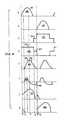
- FIG. 4 discloses current and voltage waveforms useful in explaining the operation of the converter circuit disclosed in FIG. 1;
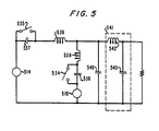
- FIG. 5 is an equivalent circuit useful in describing the operation of the circuit disclosed in FIG. 1.
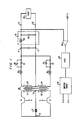
- A push pull or double ended DC to DC converter adopted to operate in a quasi resonant mode is shown in FIG. 1. A DC voltage source 10 connected to the
input terminals 11 and 12 is alternately applied to theprimary windings 21 and 22 ofpower transformer 20 through the alternate ON-OFF switching ofpower transistors secondary windings diodes capacitor 43. Aload 50 to be energized is connected tooutput terminals filter capacitor 43. - A control circuit for voltage regulation is shown which operates the switching of the two
power switching transistors output terminal 31 is coupled to a comparator 46 which is also connected to receive a reference voltage. The output error signal of the comparator 46 is applied to aduty cycle control 47 which may comprise a voltage controlled oscillator whose frequency is responsive to the magnitude of the error signal. The duty cycle control output is applied to aswitch drive circuit 48 which may comprise a monostable multivibrator in which one output is fixed in duration while the other output varies in duration in order to accomplish regulation of the output voltage. The multivibrator output is applied through a toggle gate which alternates the drive to the a and b terminals and hence to the base inputs a and b of the twoswitching transistors - The
power transformer 20 is preferably designed to have theleakage reactances secondary windings diodes - Each rectifying
diode switching transistors output load 50. While filter 41 is shown as a single stage filter, multi stage filters with similar characteristics may also be used. - This circuit and its many advantages may be readily understood by describing a typical cycle of steady state operation. The converter circuit basically operates in a two phase mode of resonant operation in which a separate quasi resonant signal processing event is independently associated with each
switching transistor switching transistors diodes switching transistors diode - The principles of the circuit are readily ascertained by referring to the various voltage and current waveforms of FIG. 4 occurring during steady state operation of the converter. Prior to the initial time T₀ shown in FIG. 4 both
switching transistors diodes diode - For the purpose of exploring circuit operation, assume that at time t₀ as shown in FIG. 4, the
transistor 14 has just been biased into a conducting state and thetransistor 15 has been nonconducting for a short interval starting prior to t₀ and for the time being remains nonconducting. A current shown bycurrent waveform 410 in FIG. 4, part A begins to flow in the circuit loop comprising the voltage source 10, transformer winding 21 and theswitching transistor 14. At this moment there is no current flow in the circuitloop including transistor 15 and hence a voltage equal in magnitude to twice the voltage of voltage source 10 appears across thetransistor 15 as shown by voltage level 441 ofvoltage waveform 440 in FIG. 4, Part D. - The current flowing through
transistor 14 has a sinusoidal wave form and continues conducting in duration sufficiently to complete a full half cycle current waveform for which eventually terminates at t₃. This is shown in current waveform in FIG. 4, part A which extends from t₀ to t₃. A current shown bywaveform 470 in FIG. 4, part 6 is flowing through the rectifyingdiode 35 and at the time t₀ has a value equal to 1/2 the output load circuit. It steadily increases in value as shown bywaveform 470 in FIG. 4, Part G to a value equaling the load current at time t₁ and eventually to a peak value at time T₂. All the current exceeding the load current is directed into the resonanting capacitor 40 as shown bywaveform 460 in FIG. 4, PartF. Rectifying diode 34 also conducts a current equaling 1/2 the load circuit at time t₀ as shown bywaveform 480 in FIG. 4, Part H. This current is decaying and reaches zero value at time t₁. Since the output filter inductor 42 acts as a constant current sink only a current equal to the steady state load current is transmitted into theload 50 and any excess current is directed into the resonating capacitor 40. This charging current is shown bywaveform 460 in FIG. 4, Part F, and is shown extending between times t₁ and t₄. It completes a 3/4 period sine wave function at time t₃ which is followed by a fixed charging current which abruptly terminates at t₄. - At time t₁ the current in the switching
transistor 14 and in the associated conducting rectifyingdiode 35 is at a value substantially equal to the full load current, as shown inwaveform 470 in FIG. 4, Part H, ramp 490. The current indiode 34, as shown bywaveform 480 in FIG. 4, Part H has decayed to zero by timet₁ leaving diode 34 fully reverse biased and nonconducting. After time t₁ continues to increase in bothtransistor 14 and diode 35 a charging current as shown bywaveform 460 in FIG. 4, Part F begins to flow into the resonating capacitor 40 causing its voltage to rise along curve 451 as shown bywaveform 450 in FIG. 4, Part E. - During the time interval from t₁ to t₃ the current in conducting
transistor 14 rises to its peak value at time t₂ as shown bypoint 411 and the capacitor 40 is also charged to its peak value at this same time t₂ as shown bypoint 452 inwaveform 450. This transistor current subsequently declines to zero at time t₃, and immediately subsequent to this time t₃, the charging current flowing through capacitor 40 goes negative and declines to a negative value equaling the load current magnitude at time t₄ as shown bywaveform 460 in FIG. 4, Part F. - At time t₃ the
transistor 14 is biased nonconducting and current flow in its related circuit loop shown bywaveform 410 ceases. Similarly, current flow in the rectifyingdiode 35 shown bywaveform 470 has also dropped to zero. The charging current in the resonating capacitor 40 stabilizes at the negative value of the load circuit as shown bylevel 461 inwaveform 460 shown in FIG. 4, Part F. At the time t₄ the rectifyingdiodes waveform 460 and the voltage drop across eachtransistor voltage levels - At the end of the half cycle neither switching
transistor voltage level t 
transistor 15 begins to conduct current in agreement with thewaveform 420 in FIG. 4, Part B and the second half cycle is initiated which proceeds in a manner similar to that described for the first half cycle. - It is apparent from the foregoing description that the quasi resonant signal action is advantageously confined tot he secondary part of the converter circuit and that since each half cycle is sufficient in duration to permit the desired resonant action, the variable pulse width conduction interval on the primary side may be operated over a considerable range without adversely affecting the resonant properties of the circuit. A particular feature of this arrangement is the parasitic capacitance of the rectifying diode that shunts the rectifying diode and the leakage inductance associated with the idle resonant circuit which in any half cycle functions as a harmonic filter and limits the application of harmonics to the resonanting capacitor 40.
- A half bridge embodiment of a power train embodying the principles of the invention is shown in a schematic form in FIG. 3 in which two alternately conducting
transistor switches DC voltage source 210 and theinput voltage terminals 211 and 212. The switched output voltage is taken from thejunction node 216 of the two switchingtransistors transformer 220. A resonant secondary circuit identical to the FIG. 1 is alternately energized bysecondary windings - A full bridge embodiment of the inverter is shown in FIG. 3 which includes four switching
transistors transformer 320. The secondary portion of the circuit is substantially identical in circuitry and operation to that shown for FIG. 1. - An equivalent circuit showing the electrical functional operation of the circuit schematic of FIG. 1 is shown in FIG. 5. The power transformer is not shown and hence a unity transformation ratio is assumed. The two oppositely phased resonant circuits are shown as having oppositely phased voltage
pulse source circuits voltage pulse source 514 includes a switch 535 which is operated as a diode switch, acapacitance 537 shunting the switch and aninductance 539. The second resonant circuit coupled tovoltage pulse source 515 includes thediode switch 534, a capacitance 536 shunting the switch and aninductance 538. - The two pulse voltage sources are operated during oppositely phased intervals as that the two oppositely phased resonant circuits are pulsed or pumped alternately during oppositely phased intervals. Each resonant circuit shares a common
resonant capacitor 540 which is connected at the input to theoutput filter 541 which includesinductor 542 andcapacitor 543. As each resonant circuit is pulsed, the inductor of that circuit resonates withinresonant capacitor 540 for substantially a half cycle of operation with subsequent resonance being cut off by the opening of the associated/switch diode. The inductor and capacitor of the nonresonating circuit in the opposite phase operates as a harmonic filter to reduce harmonics being applied to the resonatingcapacitor 540. Operation of the circuit at FIG. 5 may be further specified in terms of the following equations specifying the response and conditions of operation of the resonant circuits.

CR is the capacitance of the resonatingcapacitor 540.
VMAX is the maximum voltage applied by the source (514) to the resonant network.
Lmatching is the inductance of output filter 41.
VCR is the voltage across the resonatingcapacitor C R 540.
ICR is the current through the resonatingcapacitor C R 540.
LR is theleakage reactance
VLR is the voltage across the leakage reactance LR, 538 or 539.
ILR is the current through the leakage reactance LR, 538 or 539.
ZTON(LC) is defined as equal to
Claims (5)
1. A power converter comprising:
input means for accepting a DC voltage source,
a power transformer including a primary winding and a secondary winding;
a first switch for applying the voltage source to the primary winding in a first direction;
a second switch for applying the DC voltage source to the primary winding in a second direction opposite the first direction;
characterized by:
a first secondary resonant circuit connected to a first terminal of the secondary winding and including, a first inductance derived in part from a leakage inductance of the transformer, a first rectifying diode and a first capacitance access port;
a second secondary resonant circuit connected to a second terminal of the secondary winding and including, a second inductance derived in part from a leakage inductance of the transformer, a second rectifying diode and a second capacitance access port;
a resonating capacitor connecting the first and second capacitance access port and having resonant operation with both the first and second resonant circuits; and
output means connected to the resonating capacitor, having constant current sink characteristics and adopted for accepting a load to be energized.
2. A power converter as defined in claim 1 and further characterized wherein the first and second switch connect a first node of the input means to opposite terminals of the primary winding respectively and a second node of the input means connected to a node of the primary winding intermediate the opposite terminals of the primary winding.
3. A power converter as defined in claim 1 and further characterized wherein the first and second switch are connected in a series connection and the series correction being connected in shunt with the input means.
4. A power converter as defined in claim 1 and further characterized in that the first and second switches are connected in a bridge configuration with a third switch connected in the bridge configuration operating in accord with the first switch and a fourth switch connected in the bridge configuration operating in accord with the second switch.
5. A power converter as defined in claim 1 and further characterized by including regulation control circuitry, comprising:
means for sensing an output signal of the load
means responsive to the means for sensing for generating an error signal responsive to a deviation of the output signal from a predetermined regulation value, and
means for converting the error signal into a frequency, and
means responsive to the frequency to generate a driver signal having a fixed interval value and a variable period, and
means for alternately applying the drive signal to the first and second switches.
Applications Claiming Priority (2)
| Application Number | Priority Date | Filing Date | Title |
|---|---|---|---|
| US43008 | 1987-04-27 | ||
| US07/043,008 US4823249A (en) | 1987-04-27 | 1987-04-27 | High-frequency resonant power converter |
Publications (2)
| Publication Number | Publication Date |
|---|---|
| EP0289196A2 true EP0289196A2 (en) | 1988-11-02 |
| EP0289196A3 EP0289196A3 (en) | 1989-10-04 |
Family
ID=21924965
Family Applications (1)
| Application Number | Title | Priority Date | Filing Date |
|---|---|---|---|
| EP88303521A Withdrawn EP0289196A3 (en) | 1987-04-27 | 1988-04-19 | High frequency resonant power converter |
Country Status (5)
| Country | Link |
|---|---|
| US (1) | US4823249A (en) |
| EP (1) | EP0289196A3 (en) |
| JP (1) | JPH0197169A (en) |
| KR (1) | KR880013300A (en) |
| CA (1) | CA1301837C (en) |
Cited By (4)
| Publication number | Priority date | Publication date | Assignee | Title |
|---|---|---|---|---|
| EP0508664A1 (en) * | 1991-04-10 | 1992-10-14 | Lambda Electronics, Inc. | DC to DC converter |
| WO1997008812A1 (en) * | 1995-08-30 | 1997-03-06 | Gaia Converter | Direct current voltage converter with soft switching |
| USRE36571E (en) * | 1993-04-29 | 2000-02-15 | Lucent Technologies Inc. | Low loss synchronous rectifier for application to clamped-mode power converters |
| US10199950B1 (en) | 2013-07-02 | 2019-02-05 | Vlt, Inc. | Power distribution architecture with series-connected bus converter |
Families Citing this family (78)
| Publication number | Priority date | Publication date | Assignee | Title |
|---|---|---|---|---|
| KR890702327A (en) * | 1987-10-29 | 1989-12-23 | 원본미기재 | Zero Voltage Switching DC-AC Inverter or Converter |
| FR2627644B1 (en) * | 1988-02-24 | 1991-05-03 | Europ Agence Spatiale | CONTINUOUS-CONTINUOUS CONVERTER WITHOUT LOSS OF SWITCHING, IN PARTICULAR FOR HIGH FREQUENCY CONTINUOUS SUPPLY OR FOR PROGRESSIVE WAVE TUBE AMPLIFIER |
| US5396410A (en) * | 1990-01-31 | 1995-03-07 | Kabushiki Kaisha Toshiba | Zero current switching resonant converter |
| US4984146A (en) * | 1990-03-27 | 1991-01-08 | International Business Machines Corporation | Suppression of radiated EMI for power supplies |
| US5132888A (en) * | 1991-01-07 | 1992-07-21 | Unisys Corporation | Interleaved bridge converter |
| JP3132093B2 (en) * | 1991-09-25 | 2001-02-05 | ヤマハ株式会社 | Power supply circuit |
| US5177675A (en) * | 1991-10-16 | 1993-01-05 | Shindengen Archer Corp. | Zero voltage, zero current, resonant converter |
| DE4234772A1 (en) * | 1992-10-15 | 1994-04-21 | Ant Nachrichtentech | Method for operating a voltage converter and voltage converter and application |
| US5521807A (en) * | 1992-12-31 | 1996-05-28 | Interpoint Corporation | DC-To-DC converter with secondary flyback core reset |
| US5485362A (en) * | 1993-09-08 | 1996-01-16 | Eos Corporation | Resonant power converter for changing the magnitude of a DC voltage |
| US5546295A (en) * | 1994-02-24 | 1996-08-13 | Rotron Incorporated | Electrical power converter, power supply, and inverter with series-connected switching circuits |
| US7269034B2 (en) | 1997-01-24 | 2007-09-11 | Synqor, Inc. | High efficiency power converter |
| US5903448A (en) * | 1997-08-20 | 1999-05-11 | Lucent Technologies Inc. | Four quadrant flyback converter, method of operation thereof and power plant employing the same |
| US5872703A (en) * | 1997-08-25 | 1999-02-16 | The Charles Machine Works, Inc. | System and method for regulating power in tank circuits having a bridge configuration |
| US5909362A (en) * | 1998-01-12 | 1999-06-01 | Eldec Corporation | Resonant power converter |
| GB2335317A (en) * | 1998-03-11 | 1999-09-15 | Simon Richard Greenwood | Bi-directional voltage converter |
| WO2000024456A1 (en) | 1998-10-27 | 2000-05-04 | Phillips Richard P | Transcutaneous energy transmission system with full wave class e rectifier |
| CA2377503A1 (en) | 1999-06-30 | 2001-01-11 | Peco Ii, Inc. | Diode recovery current suppression circuits |
| US6442047B1 (en) | 1999-10-08 | 2002-08-27 | Lambda Electronics, Inc. | Power conversion apparatus and methods with reduced current and voltage switching |
| WO2001076053A1 (en) * | 2000-04-03 | 2001-10-11 | Aalborg Universitet | A resonant converter |
| JP4556331B2 (en) * | 2001-01-22 | 2010-10-06 | 株式会社豊田自動織機 | Switching power supply circuit |
| US6807073B1 (en) | 2001-05-02 | 2004-10-19 | Oltronics, Inc. | Switching type power converter circuit and method for use therein |
| EP1303032A3 (en) * | 2001-09-04 | 2005-02-09 | Philips Intellectual Property & Standards GmbH | Control device for a resonant converter |
| TWI263395B (en) * | 2001-11-02 | 2006-10-01 | Delta Electronics Inc | Power supply device |
| US7046523B2 (en) * | 2002-04-18 | 2006-05-16 | Coldwatt, Inc. | Core structure and interleaved DC—DC converter topology |
| US7280026B2 (en) | 2002-04-18 | 2007-10-09 | Coldwatt, Inc. | Extended E matrix integrated magnetics (MIM) core |
| US7321283B2 (en) * | 2004-08-19 | 2008-01-22 | Coldwatt, Inc. | Vertical winding structures for planar magnetic switched-mode power converters |
| US7427910B2 (en) * | 2004-08-19 | 2008-09-23 | Coldwatt, Inc. | Winding structure for efficient switch-mode power converters |
| US7417875B2 (en) * | 2005-02-08 | 2008-08-26 | Coldwatt, Inc. | Power converter employing integrated magnetics with a current multiplier rectifier and method of operating the same |
| US7385375B2 (en) * | 2005-02-23 | 2008-06-10 | Coldwatt, Inc. | Control circuit for a depletion mode switch and method of operating the same |
| US7176662B2 (en) * | 2005-02-23 | 2007-02-13 | Coldwatt, Inc. | Power converter employing a tapped inductor and integrated magnetics and method of operating the same |
| US7876191B2 (en) * | 2005-02-23 | 2011-01-25 | Flextronics International Usa, Inc. | Power converter employing a tapped inductor and integrated magnetics and method of operating the same |
| CN100426056C (en) * | 2005-08-26 | 2008-10-15 | 鸿富锦精密工业(深圳)有限公司 | Multiple lamp tube driving system and method |
| US8595041B2 (en) * | 2006-02-07 | 2013-11-26 | Sap Ag | Task responsibility system |
| US8125205B2 (en) * | 2006-08-31 | 2012-02-28 | Flextronics International Usa, Inc. | Power converter employing regulators with a coupled inductor |
| US7667986B2 (en) * | 2006-12-01 | 2010-02-23 | Flextronics International Usa, Inc. | Power system with power converters having an adaptive controller |
| US7675759B2 (en) * | 2006-12-01 | 2010-03-09 | Flextronics International Usa, Inc. | Power system with power converters having an adaptive controller |
| US7675758B2 (en) * | 2006-12-01 | 2010-03-09 | Flextronics International Usa, Inc. | Power converter with an adaptive controller and method of operating the same |
| US7889517B2 (en) * | 2006-12-01 | 2011-02-15 | Flextronics International Usa, Inc. | Power system with power converters having an adaptive controller |
| US9197132B2 (en) | 2006-12-01 | 2015-11-24 | Flextronics International Usa, Inc. | Power converter with an adaptive controller and method of operating the same |
| US7468649B2 (en) * | 2007-03-14 | 2008-12-23 | Flextronics International Usa, Inc. | Isolated power converter |
| US7906941B2 (en) * | 2007-06-19 | 2011-03-15 | Flextronics International Usa, Inc. | System and method for estimating input power for a power processing circuit |
| US8693213B2 (en) * | 2008-05-21 | 2014-04-08 | Flextronics Ap, Llc | Resonant power factor correction converter |
| US8531174B2 (en) * | 2008-06-12 | 2013-09-10 | Flextronics Ap, Llc | AC-DC input adapter |
| CN102342008B (en) | 2009-01-19 | 2016-08-03 | 伟创力国际美国公司 | Controller for power converter |
| US8520414B2 (en) * | 2009-01-19 | 2013-08-27 | Power Systems Technologies, Ltd. | Controller for a power converter |
| CN102356438B (en) | 2009-03-31 | 2014-08-27 | 伟创力国际美国公司 | Magnetic device formed with u-shaped core pieces and power converter employing the same |
| US8514593B2 (en) * | 2009-06-17 | 2013-08-20 | Power Systems Technologies, Ltd. | Power converter employing a variable switching frequency and a magnetic device with a non-uniform gap |
| US9077248B2 (en) | 2009-06-17 | 2015-07-07 | Power Systems Technologies Ltd | Start-up circuit for a power adapter |
| US8643222B2 (en) | 2009-06-17 | 2014-02-04 | Power Systems Technologies Ltd | Power adapter employing a power reducer |
| US8891803B2 (en) * | 2009-06-23 | 2014-11-18 | Flextronics Ap, Llc | Notebook power supply with integrated subwoofer |
| US8638578B2 (en) | 2009-08-14 | 2014-01-28 | Power System Technologies, Ltd. | Power converter including a charge pump employable in a power adapter |
| US8976549B2 (en) * | 2009-12-03 | 2015-03-10 | Power Systems Technologies, Ltd. | Startup circuit including first and second Schmitt triggers and power converter employing the same |
| US8520420B2 (en) * | 2009-12-18 | 2013-08-27 | Power Systems Technologies, Ltd. | Controller for modifying dead time between switches in a power converter |
| US9246391B2 (en) | 2010-01-22 | 2016-01-26 | Power Systems Technologies Ltd. | Controller for providing a corrected signal to a sensed peak current through a circuit element of a power converter |
| US8787043B2 (en) * | 2010-01-22 | 2014-07-22 | Power Systems Technologies, Ltd. | Controller for a power converter and method of operating the same |
| US8767418B2 (en) | 2010-03-17 | 2014-07-01 | Power Systems Technologies Ltd. | Control system for a power converter and method of operating the same |
| US8964413B2 (en) * | 2010-04-22 | 2015-02-24 | Flextronics Ap, Llc | Two stage resonant converter enabling soft-switching in an isolated stage |
| US8488340B2 (en) | 2010-08-27 | 2013-07-16 | Flextronics Ap, Llc | Power converter with boost-buck-buck configuration utilizing an intermediate power regulating circuit |
| US8441810B2 (en) | 2010-11-09 | 2013-05-14 | Flextronics Ap, Llc | Cascade power system architecture |
| US8520410B2 (en) | 2010-11-09 | 2013-08-27 | Flextronics Ap, Llc | Virtual parametric high side MOSFET driver |
| US9054602B2 (en) * | 2010-12-10 | 2015-06-09 | Helen Pollock | Resonant circuit with constant current characteristics |
| US8792257B2 (en) | 2011-03-25 | 2014-07-29 | Power Systems Technologies, Ltd. | Power converter with reduced power dissipation |
| US8842450B2 (en) | 2011-04-12 | 2014-09-23 | Flextronics, Ap, Llc | Power converter using multiple phase-shifting quasi-resonant converters |
| US8792256B2 (en) | 2012-01-27 | 2014-07-29 | Power Systems Technologies Ltd. | Controller for a switch and method of operating the same |
| US9190898B2 (en) | 2012-07-06 | 2015-11-17 | Power Systems Technologies, Ltd | Controller for a power converter and method of operating the same |
| US9379629B2 (en) | 2012-07-16 | 2016-06-28 | Power Systems Technologies, Ltd. | Magnetic device and power converter employing the same |
| US9099232B2 (en) | 2012-07-16 | 2015-08-04 | Power Systems Technologies Ltd. | Magnetic device and power converter employing the same |
| US9214264B2 (en) | 2012-07-16 | 2015-12-15 | Power Systems Technologies, Ltd. | Magnetic device and power converter employing the same |
| US9106130B2 (en) | 2012-07-16 | 2015-08-11 | Power Systems Technologies, Inc. | Magnetic device and power converter employing the same |
| WO2014074923A1 (en) * | 2012-11-09 | 2014-05-15 | Murata Manufacturing Co., Ltd. | Soft-start for resonant converters |
| US9240712B2 (en) | 2012-12-13 | 2016-01-19 | Power Systems Technologies Ltd. | Controller including a common current-sense device for power switches of a power converter |
| CN103337964A (en) * | 2013-04-27 | 2013-10-02 | 南京航空航天大学 | Ultrahigh frequency isolation push-pull resonant power converter |
| JP6242654B2 (en) * | 2013-10-23 | 2017-12-06 | 東芝テック株式会社 | Power converter |
| DE102013223194A1 (en) * | 2013-11-14 | 2015-05-21 | Robert Bosch Gmbh | DC-DC converter, method for clocking a converter of a DC-DC converter and method for converting DC voltage |
| FR3020523B1 (en) * | 2014-04-29 | 2016-05-06 | Valeo Systemes De Controle Moteur | ELECTRICAL POWER SUPPLY AND METHOD FOR CONTROLLING AN ELECTRIC POWER SUPPLY |
| US10389104B1 (en) * | 2015-01-09 | 2019-08-20 | Clemson University | Circuit breaker for DC circuits using coupled induction |
| CN110932557B (en) * | 2019-11-29 | 2021-01-12 | 山东科技大学 | High-gain quasi-resonant DC-DC converter based on voltage doubling rectifying circuit |
Citations (3)
| Publication number | Priority date | Publication date | Assignee | Title |
|---|---|---|---|---|
| GB1431262A (en) * | 1971-12-16 | 1976-04-07 | Advance Electronics Ltd | Power supply apparatus |
| US4017784A (en) * | 1976-05-17 | 1977-04-12 | Litton Systems, Inc. | DC to DC converter |
| WO1982003302A1 (en) * | 1981-03-20 | 1982-09-30 | Corp Vicor | Forward converter switching at zero current |
Family Cites Families (7)
| Publication number | Priority date | Publication date | Assignee | Title |
|---|---|---|---|---|
| US3089077A (en) * | 1958-10-06 | 1963-05-07 | Basler Electric Co | Transistor converters |
| JPS5746673A (en) * | 1980-09-05 | 1982-03-17 | Kosuke Harada | Dc-dc converter |
| JPS5846874A (en) * | 1981-09-12 | 1983-03-18 | Hitachi Heating Appliance Co Ltd | Converter for automobile |
| US4685041A (en) * | 1985-03-11 | 1987-08-04 | American Telephone And Telegraph Company, At&T Bell Laboratories | Resonant rectifier circuit |
| US4628426A (en) * | 1985-10-31 | 1986-12-09 | General Electric Company | Dual output DC-DC converter with independently controllable output voltages |
| US4720667A (en) * | 1986-06-20 | 1988-01-19 | Lee Fred C | Zero-current switching quasi-resonant converters operating in a full-wave mode |
| US4720668A (en) * | 1986-06-20 | 1988-01-19 | Lee Fred C | Zero-voltage switching quasi-resonant converters |
-
1987
- 1987-04-27 US US07/043,008 patent/US4823249A/en not_active Expired - Lifetime
-
1988
- 1988-03-29 CA CA000562761A patent/CA1301837C/en not_active Expired - Fee Related
- 1988-04-19 EP EP88303521A patent/EP0289196A3/en not_active Withdrawn
- 1988-04-25 KR KR1019880004686A patent/KR880013300A/en not_active Application Discontinuation
- 1988-04-27 JP JP63102845A patent/JPH0197169A/en active Pending
Patent Citations (3)
| Publication number | Priority date | Publication date | Assignee | Title |
|---|---|---|---|---|
| GB1431262A (en) * | 1971-12-16 | 1976-04-07 | Advance Electronics Ltd | Power supply apparatus |
| US4017784A (en) * | 1976-05-17 | 1977-04-12 | Litton Systems, Inc. | DC to DC converter |
| WO1982003302A1 (en) * | 1981-03-20 | 1982-09-30 | Corp Vicor | Forward converter switching at zero current |
Non-Patent Citations (2)
| Title |
|---|
| APEC'86 28 April 1986, New Orleans, Luisiana page 83 - 89; K. LIU et al: "Secondary-side resonance for high-frequency power conversion" * |
| APEC'87 06 March 1987, San Diego, California page 105 - 114; D.C. HOPKINS et al: "Two-megahertz off-line hybridized quasi-resonant converter" * |
Cited By (9)
| Publication number | Priority date | Publication date | Assignee | Title |
|---|---|---|---|---|
| EP0508664A1 (en) * | 1991-04-10 | 1992-10-14 | Lambda Electronics, Inc. | DC to DC converter |
| US5291382A (en) * | 1991-04-10 | 1994-03-01 | Lambda Electronics Inc. | Pulse width modulated DC/DC converter with reduced ripple current coponent stress and zero voltage switching capability |
| USRE36571E (en) * | 1993-04-29 | 2000-02-15 | Lucent Technologies Inc. | Low loss synchronous rectifier for application to clamped-mode power converters |
| WO1997008812A1 (en) * | 1995-08-30 | 1997-03-06 | Gaia Converter | Direct current voltage converter with soft switching |
| FR2738417A1 (en) * | 1995-08-30 | 1997-03-07 | Gaia Converter | CONTINUOUSLY SWITCHED VOLTAGE CONVERTER |
| US10199950B1 (en) | 2013-07-02 | 2019-02-05 | Vlt, Inc. | Power distribution architecture with series-connected bus converter |
| US10594223B1 (en) | 2013-07-02 | 2020-03-17 | Vlt, Inc. | Power distribution architecture with series-connected bus converter |
| US11075583B1 (en) | 2013-07-02 | 2021-07-27 | Vicor Corporation | Power distribution architecture with series-connected bus converter |
| US11705820B2 (en) | 2013-07-02 | 2023-07-18 | Vicor Corporation | Power distribution architecture with series-connected bus converter |
Also Published As
| Publication number | Publication date |
|---|---|
| KR880013300A (en) | 1988-11-30 |
| JPH0197169A (en) | 1989-04-14 |
| CA1301837C (en) | 1992-05-26 |
| EP0289196A3 (en) | 1989-10-04 |
| US4823249A (en) | 1989-04-18 |
Similar Documents
| Publication | Publication Date | Title |
|---|---|---|
| US4823249A (en) | High-frequency resonant power converter | |
| US5140510A (en) | Constant frequency power converter | |
| US6738267B1 (en) | Switched power supply converter with a piezoelectric transformer | |
| EP0508664B1 (en) | DC to DC converter | |
| US4814962A (en) | Zero voltage switching half bridge resonant converter | |
| US4677534A (en) | Stabilizing power source apparatus | |
| US5510974A (en) | High frequency push-pull converter with input power factor correction | |
| US5132888A (en) | Interleaved bridge converter | |
| EP0334100B1 (en) | Full bridge switching circuit | |
| USRE37889E1 (en) | Low loss synchronous rectifier for application to clamped-mode power converters | |
| US5923152A (en) | Power factor correction circuit with soft switched boost converter | |
| US4845605A (en) | High-frequency DC-DC power converter with zero-voltage switching of single primary-side power device | |
| EP0851566A2 (en) | Half-bridge zero-voltage-switched PWM flyback DC/DC converter | |
| US4493017A (en) | Single drive transformer with regenerative winding for p.w.m. supply having alternately conducting power devices | |
| US5282122A (en) | High voltage power supply topology suited for miniaturization | |
| US5504668A (en) | Frequency controlled resonant inverter | |
| WO1991000643A1 (en) | Ac/dc conversion with reduced supply waveform distortion | |
| US5303137A (en) | Multiresonant self-oscillating converter circuit | |
| US4688165A (en) | Current fed inverter bridge with conduction overlap and load tuning | |
| US5523936A (en) | Built-in input filter forward converter | |
| US4951186A (en) | Single-ended forward frequency converter with a transformer and a demagnetization means | |
| US4176392A (en) | Series induction/parallel inverter power stage and power staging method for DC-DC power converter | |
| GB2155255A (en) | Inverter for feeding a load having an inductive component | |
| US5936851A (en) | Regulated resonant converter | |
| JP2003134817A (en) | Power supply |
Legal Events
| Date | Code | Title | Description |
|---|---|---|---|
| PUAI | Public reference made under article 153(3) epc to a published international application that has entered the european phase |
Free format text: ORIGINAL CODE: 0009012 |
|
| AK | Designated contracting states |
Kind code of ref document: A2 Designated state(s): DE FR GB IT SE |
|
| PUAL | Search report despatched |
Free format text: ORIGINAL CODE: 0009013 |
|
| AK | Designated contracting states |
Kind code of ref document: A3 Designated state(s): DE FR GB IT SE |
|
| STAA | Information on the status of an ep patent application or granted ep patent |
Free format text: STATUS: THE APPLICATION IS DEEMED TO BE WITHDRAWN |
|
| 18D | Application deemed to be withdrawn |
Effective date: 19900405 |