EP0287055A2 - Liquid crystal display device - Google Patents
Liquid crystal display device Download PDFInfo
- Publication number
- EP0287055A2 EP0287055A2 EP88105868A EP88105868A EP0287055A2 EP 0287055 A2 EP0287055 A2 EP 0287055A2 EP 88105868 A EP88105868 A EP 88105868A EP 88105868 A EP88105868 A EP 88105868A EP 0287055 A2 EP0287055 A2 EP 0287055A2
- Authority
- EP
- European Patent Office
- Prior art keywords
- liquid crystal
- video signal
- electrodes
- numbered
- signal
- Prior art date
- Legal status (The legal status is an assumption and is not a legal conclusion. Google has not performed a legal analysis and makes no representation as to the accuracy of the status listed.)
- Granted
Links
Images


Classifications
-
- G—PHYSICS
- G09—EDUCATION; CRYPTOGRAPHY; DISPLAY; ADVERTISING; SEALS
- G09G—ARRANGEMENTS OR CIRCUITS FOR CONTROL OF INDICATING DEVICES USING STATIC MEANS TO PRESENT VARIABLE INFORMATION
- G09G3/00—Control arrangements or circuits, of interest only in connection with visual indicators other than cathode-ray tubes
- G09G3/20—Control arrangements or circuits, of interest only in connection with visual indicators other than cathode-ray tubes for presentation of an assembly of a number of characters, e.g. a page, by composing the assembly by combination of individual elements arranged in a matrix no fixed position being assigned to or needed to be assigned to the individual characters or partial characters
- G09G3/34—Control arrangements or circuits, of interest only in connection with visual indicators other than cathode-ray tubes for presentation of an assembly of a number of characters, e.g. a page, by composing the assembly by combination of individual elements arranged in a matrix no fixed position being assigned to or needed to be assigned to the individual characters or partial characters by control of light from an independent source
- G09G3/36—Control arrangements or circuits, of interest only in connection with visual indicators other than cathode-ray tubes for presentation of an assembly of a number of characters, e.g. a page, by composing the assembly by combination of individual elements arranged in a matrix no fixed position being assigned to or needed to be assigned to the individual characters or partial characters by control of light from an independent source using liquid crystals
- G09G3/3607—Control arrangements or circuits, of interest only in connection with visual indicators other than cathode-ray tubes for presentation of an assembly of a number of characters, e.g. a page, by composing the assembly by combination of individual elements arranged in a matrix no fixed position being assigned to or needed to be assigned to the individual characters or partial characters by control of light from an independent source using liquid crystals for displaying colours or for displaying grey scales with a specific pixel layout, e.g. using sub-pixels
-
- G—PHYSICS
- G09—EDUCATION; CRYPTOGRAPHY; DISPLAY; ADVERTISING; SEALS
- G09G—ARRANGEMENTS OR CIRCUITS FOR CONTROL OF INDICATING DEVICES USING STATIC MEANS TO PRESENT VARIABLE INFORMATION
- G09G3/00—Control arrangements or circuits, of interest only in connection with visual indicators other than cathode-ray tubes
- G09G3/20—Control arrangements or circuits, of interest only in connection with visual indicators other than cathode-ray tubes for presentation of an assembly of a number of characters, e.g. a page, by composing the assembly by combination of individual elements arranged in a matrix no fixed position being assigned to or needed to be assigned to the individual characters or partial characters
- G09G3/34—Control arrangements or circuits, of interest only in connection with visual indicators other than cathode-ray tubes for presentation of an assembly of a number of characters, e.g. a page, by composing the assembly by combination of individual elements arranged in a matrix no fixed position being assigned to or needed to be assigned to the individual characters or partial characters by control of light from an independent source
- G09G3/36—Control arrangements or circuits, of interest only in connection with visual indicators other than cathode-ray tubes for presentation of an assembly of a number of characters, e.g. a page, by composing the assembly by combination of individual elements arranged in a matrix no fixed position being assigned to or needed to be assigned to the individual characters or partial characters by control of light from an independent source using liquid crystals
- G09G3/3611—Control of matrices with row and column drivers
- G09G3/3648—Control of matrices with row and column drivers using an active matrix
-
- G—PHYSICS
- G09—EDUCATION; CRYPTOGRAPHY; DISPLAY; ADVERTISING; SEALS
- G09G—ARRANGEMENTS OR CIRCUITS FOR CONTROL OF INDICATING DEVICES USING STATIC MEANS TO PRESENT VARIABLE INFORMATION
- G09G3/00—Control arrangements or circuits, of interest only in connection with visual indicators other than cathode-ray tubes
- G09G3/20—Control arrangements or circuits, of interest only in connection with visual indicators other than cathode-ray tubes for presentation of an assembly of a number of characters, e.g. a page, by composing the assembly by combination of individual elements arranged in a matrix no fixed position being assigned to or needed to be assigned to the individual characters or partial characters
- G09G3/34—Control arrangements or circuits, of interest only in connection with visual indicators other than cathode-ray tubes for presentation of an assembly of a number of characters, e.g. a page, by composing the assembly by combination of individual elements arranged in a matrix no fixed position being assigned to or needed to be assigned to the individual characters or partial characters by control of light from an independent source
- G09G3/36—Control arrangements or circuits, of interest only in connection with visual indicators other than cathode-ray tubes for presentation of an assembly of a number of characters, e.g. a page, by composing the assembly by combination of individual elements arranged in a matrix no fixed position being assigned to or needed to be assigned to the individual characters or partial characters by control of light from an independent source using liquid crystals
- G09G3/3611—Control of matrices with row and column drivers
- G09G3/3614—Control of polarity reversal in general
Definitions
- the present invention generally relates to liquid crystal display devices and, more particularly, to a liquid crystal display device adapted to be driven by a television signal.
- FIG. 19 of the accompanying drawings illustrates, in the form of an equivalent circuit, the typical prior art liquid crystal display device. Reference to Fig. 19 will now be made for the purpose of discussion of the prior art which is believed to be pertinent to the present invention.
- the prior art liquid crystal display device shown in Fig. 19 comprises a plurality of liquid crystal cells 1, each shown in the form of an equivalent capacitor, display electrodes 2 thereof and mating counter electrodes 3.
- a thin film transistor 4 of MIS structure is connected to each liquid crystal cell 1 as a switching active element for driving the respective liquid crystal cell 1.
- the liquid crystal cells 1 and the thin film transistors 4 are arranged in a matrix having a plurality of, for example, four, rows of source lines S1, S2, S3 and S4 and a plurality of, for example, four, columns of control lines G1, G2, G3 and G4, only a portion of which is shown in Fig. 19.
- the transistors 4 in each of the first to fourth rows have their gates connected to the associated control line G1, G2, G3 or G4.
- the first to fourth control lines are adapted to be scanned according to an interlaced scanning scheme so that the first and third control lines G1 and G3 can be excited by odd-numbered line scanning of the television signal whereas the second and fourth control lines G2 and G4 can be excited by even-numbered line scanning of the same television signal.
- a predetermined voltage inverted for each frame is applied to the counter electrodes of the respective liquid crystal cells 1 as a drive voltage.
- Video signals (for example, R, G and B signals) to be displayed are supplied through the source lines S1 to S4.
- the first and third control lines are successively excited by a scanning signal (line sequence pulses conforming to a horizontal synchronizing signal) so that a video signal voltage can be sequentially applied to the liquid crystal cells in the first row and the liquid crystal cells in the third row.
- a scanning signal line sequence pulses conforming to a horizontal synchronizing signal
- the second and fourth rows are sequentially scanned with the consequence that the video signal is applied to the liquid crystal cells in the second and fourth rows.
- the transistors in each of the first and third rows are switched off and the signal at the odd-numbered field is remains retained.
- the liquid crystal drive frequency will be 15 Hz if the television signal according to NTSC system is used to drive the liquid crystal cells. This is partly because the television signal is based on the interlaced scanning scheme in which the odd-numbered and even-numbered horizontal lines of the screen are scanned for each different field and partly because the electric field applied to the liquid crystal cells 1 is required to be cyclically reversed in view of the lifetime. Considering one picture element for facilitating a better understanding, the application of a positive voltage between both electrodes of each cell is repeated at intervals of four fields.
- the picture element referred to above is, after having been scanned at a n-th field, will not be scanned at the next succeeding, (n+1)th field for the purpose of interlacing; will be scanned at the subsequent (n+2)th field while applied with a negative voltage in view of the lifetime of the liquid crystal cells; and will not be scanned at the (n+3)th field for the purpose of interlacing.
- the liquid crystal cell of the picture element is again applied with a positive voltage.
- the application of the positive voltage to each liquid crystal cell takes place at intervals of the four fields which, in terms of the drive frequency, correspond to 15 Hz according to the NTSC system or 12.5 Hz according to the PAL system.
- the liquid crystal drive frequency will become one half the frame frequency, that is, 15 Hz, when display is effected based on the interlaced scanning scheme. While the frequency of 30 Hz will not be perceived as a flicker by human eyes, the frequency of 15 Hz is recognized as a flicker appearing on the screen and, as a result thereof, a picture uncomfortable to look will be reproduced.
- a drive method has been suggested wherein a combination of each two of the rows is changed for each field so that every two rows can be simultaneously driven by the same video signal.
- the drive frequency can be improved to 30 Hz, no improvement has been made in the number of effective display scanning lines per field. Specifically, assuming that the number of the effective display scanning lines driven by the same signal is 480 lines, the number of the effective display scanning lines per field remains 240 lines and, accordingly, the vertical resolution is still insufficient.
- this method has problems in that the use of a memory having a large memory capacity corresponding to the number of the display liquid crystal cells c is required and that a high speed is required in the clock frequency for a drive driver for driving active elements, resulting in the increased manufacturing cost.
- the present invention has been devised with a view to providing an improved liquid crystal display device effective to substantially eliminating the above discussed problems inherent in the prior art liquid crystal display devices.
- Another important object of the present invention is to provide an improved active matrix type liquid crystal display device of the type referred to above, which is effective to accomplish a reproduction of a picture with no flicker occurring and with no vertical resolution being lowered.
- a further object of the present invention is to provide an improved liquid crystal display device of the type referred to above, which does not require the use of the memory having a large memory capacity and the high speed clock frequency.
- a still further object of the present invention is to provide an improved liquid crystal display device of the type referred to above, wherein a bias voltage is applied to the counter electrodes in correspondence with the polarity of the video signal then reversed for each neighboring liquid crystal cells thereby to accomplish a high-contrast picture reproduction without flicker being accompanied.
- a yet further object of the present invention is to provide an improved liquid crystal display device of the type referred to above, wherein no possible shortcircuiting will occur at each point of intersections of lines and wherein a high contrast ratio can be obtained even though the drive voltage is relatively low.
- an active matrix liquid crystal display device operable on an interlaced scanning scheme and having a plurality of liquid crystal cells and switching active elements for driving the liquid crystal cells, said liquid crystal cells and said switching active elements being arranged in a matrix fashion having rows and columns intersecting with each other, which device comprises a plurality of sets, each comprised of each neighboring members of the rows of the matrix; means for scanning each set with an interlaced scanning signal at any fields, odd-numbered source lines each connected with one of said row forming the respective set, even-numbered source lines each connected with the other of said row forming the respective set; and means for applying an odd-numbered field signal to said odd-numbered source line at any field time and for applying an even-numbered field signal to said even-numbered source line at any field time.
- each set of the neighboring rows can be scanned according to the interlaced scanning scheme, and one of the neighboring rows and the other of the neighboring rows are applied with odd- and even-numbered field signals at any field time, respectively. Accordingly, when one picture element is taken into consideration, it can be scanned at any field time and, therefore, the voltages applied to the opposite electrodes of the liquid crystal cells per field can be reversed in polarity. This means that the driving frequency is 30 Hz. Moreover, since the odd- and even-numbered field signals are respectively applied to the respective set of the neighboring rows, 480 scanning lines can be utilized per field if the number of effective display scanning lines is assumed to be 480 lines. Also, the scanning time per row corresponds to one horizontal period and, therefore, no high speed characteristic is required.
- an active matrix liquid crystal display device including a plurality of rows of video signal lines, a plurality of columns of scanning lines, said rows of the video signal line and the columns of the scanning lines being arranged in a matrix fashion, a picture element electrode disposed at each of intersecting points between the rows and the columns and adapted to receive a video signal through an active element, said device being adapted to be scanned according to an interlaced scanning scheme by a signal supplied through the scanning lines, which device comprises said video signal lines being comprised of a plurality of pairs of first video signal lines and a plurality of pairs of second video signal lines; a first video signal supply means for supplying a first video signal to the first video signal lines; a second video signal supply means for supplying a second video signal to the second video signal lines, said second video signal having a phase displaced a half-cycle period relative to the first video signal; a scanning signal supply means for supplying a scanning signal to each of a plurality of sets of odd- and even-numbered
- the first and second video signals have their phases displaced a half-cycle period from each other, and the first and second picture element electrodes are arranged while displaced a half-cycle period in a direction conforming to the scanning line so that each neighboring odd- and even-numbered scanning lines can be scanned. Therefore, the televised picture substantially free from the occurrence of flickers can be displayed.
- an active matrix liquid crystal display device including a plurality of rows of video signal lines, a plurality of columns of scanning lines, said rows of the video signal line and the columns of the scanning lines being arranged in a matrix fashion, a picture element electrode disposed at each of intersecting points between the rows and the columns and adapted to receive a video signal through an active element, said device being adapted to be scanned according to an interlaced scanning scheme by a signal supplied through the scanning lines, which device comprises a scanning signal supply means for supplying a signal to each of the scanning lines; a first video signal supply means for supplying a first video signal to odd-numbered columns of the video signal lines; a second video signal supply means for supplying a second video signal to even-numbered columns of the video signal lines, said second video signal having a phase displaced a half-cycle period relative to the first video signal; first and second picture element electrodes to which the first and second video signals are respectively applied; a first counter electrode confronting each of the first picture element
- the first and second video signals have their phases displaced a half-cycle period from each other and the first and second counter electrodes are arranged while displaced a half-cycle period in phase from each other, it is possible to apply a bias voltage to the counter electrodes with respect to the polarity of the video signal which is reversed for each of the odd- and even-numbered lines of the video signal. Therefore, the televised picture can be displayed at a relatively high contrast with no flicker being accompanied.
- an active matrix liquid crystal display device which has a first insulating substrate formed with thin film transistors, gate bus electrodes, common line electrodes and picture element electrodes which do not intersect with the gate bus electrodes, a second insulating substrate formed with data bus electrodes so as to confront the first insulating substrate and so as to intersect the gate bus electrodes, and a layer of liquid crystal intervening between the first and second insulating substrates, which device comprises each of said thin film transistors, which are connected to the same gate bus electrodes, having source and drain electrodes, one of said source and drain electrodes being connected with the picture element electrode and the other of said source and drain electrodes being alternately connected with two common line electrodes confronting with each other with the gate electrode intervening therebetween, said two common line electrodes being applied with voltages different in polarity from each other.
- each of the thin film transistors in each row is alternately applied with positive and negative voltages supplied through the paired common line electrodes.
- the data bus electrodes which act as counter electrodes are also alternately applied with negative and positive data signal voltages.
- the reversion of the applied voltages to the paired common line electrodes and the reversion of the data signal voltages take place for each field at a frequency of 15 Hz.
- a plurality of liquid crystal cells C11 to C44 and a corresponding number of thin film transistors T11 to T44 are arranged in a matrix form having rows and columns, each neighboring rows being paired to provide a corresponding row line pair A1 and A2, each row line pair A1 and A2 being adapted to be driven by a respective interlaced scanning signal.
- gate electrodes of the transistors T11 to T14 and T21 to T24 in the first and second rows, respectively are connected to a first control line G1 and, similarly, gate electrodes of the transistors T31 to T34 and T41 to T44 in the third and fourth rows, respectively, are connected to a second control line G2.
- Reference numeral 111 represents an odd-numbered source line driver having output signal lines S1, S3, S5 and S7 which are connected to respective source electrodes of the transistors in one of the neighboring rows forming the respective row pair, for example, in the first and third rows.
- Reference numeral 112 represents an odd-numbered source line driver having output signal lines S2, S4, S6 and S8 which are connected to respective source electrodes of the transistors in the other of the neighboring rows forming the respective row pair, that is, in the second and fourth rows.
- the odd-numbered source line driver 111 is adapted to receive red, green and blue signals Ro, Go and Bo of odd-numbered fields. Since the liquid crystal cells shown in Fig. 1 form each color picture element as shown in Fig. 5, the red signal Ro is outputted through the output lines S1 and S7, the green signal Go is outputted through the output line S3 and the blue signal Bo is outputted through the output line S5.
- the odd-numbered source line driver 112 is adapted to receive red, green and blue signals Re, Ge and Be of even-numbered fields and, therefore, the red signal Re, the green signal Ge and the blue signal Be are outputted through the output lines S2 and S8, the output line S4 and the output line S6, respectively.
- each of the source line drivers 111 and 112 includes shift registers for providing the inputs sequentially to the output lines and also includes a respective inverting means for inverting the input signals for each scanning line as shown by the waveform (d) in Fig. 4.
- reference numeral 13 represents a color separator for separating red, green and blue signals VR, VG and VB from a video signal (c) and outputting the red, green and blue signals VR, VG and VB to an analog-to-digital (A/D) converter 114 operable to convert each of those signals into a digital amount. Digital outputs from the A/D converter 114 are then supplied through real time lines 115, first delay lines 116 and second delay lines 117.
- the real time lines 115 include a digital-to-analog (D/A) converter 124 for converting the digital amount into an analog amount, a low-pass filter 126 and first and second analog gates 128 and 129, and the red, green and blue signals Ro, Go and Bo of the odd-numbered fields which have been converted into respective analog amounts are supplied to the odd-numbered source line driver 111 through the first analog gate 128 whereas the red, green and blue signals Re, Ge and Be of the even-numbered fields which have been converted into respective analog amounts are supplied to the even-numbered source line driver 112 through the second analog gate 29.
- D/A digital-to-analog
- Each of the first and second delay lines 116 and 117 includes a digital gate 118 or 119, a field memory 120 or 121 and a digital gate 122 or 123, the digital gates 122 and 123 on the first and second delay lines 116 and 117 being in turn connected to both of third and fourth analog gates 130 and 131 through a digital-to-analog converter 125 and then through a low pass filter 127.
- the third analog gate 130 has a function of providing the odd-numbered source line driver 111 with one-field preceding odd-numbered field signals whereas the fourth analog gate 131 has a function of providing the even-numbered source line driver 112 with the one-field preceding even-numbered field signals. Since the A/D converter 114 converts each color signal into an 8-bit digital amount, the digital circuit shown in Fig. 2 is effective to perform an 8-bit processing for each color signal.
- the memories 120 and 121 are operable to store respective color signal data of the odd- and even-numbered fields, respectively.
- the signal of the even-numbered field is supplied to the even-numbered source line driver 112 through the real time lines 115, whereas the one-field preceding odd-numbered field signal read out from the memory 120 is supplied to the odd-numbered source line driver 111. At this time, the signal of the even-numbered field is written in the memory 121. It is to be noted that, although in Fig.
- the A/D conversion and the subsequent D/A conversion are successivelysively effected so that, since the first and second delay lines 116 and 117 are digital circuits, real time signal on the real time lines 115 may be equally affected as in the signal processed through the digital circuits, the outputs from the color separator 113 may be supplied direct to the first and second analog gates 128 and 129 where such a consideration is not required. Also, where each of the memories 120 and 121 are employed in the form of an analog memory such as a charge-coupled device, no digital processing is required accordingly.
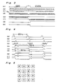
- Fig. 3 illustrates a chart of respective waveforms of gate signals appearing in the circuit of Fig. 2.
- the waveform (a) represents a vertical synchronizing signal contained in the video signal, wherein ODD and EVEN stand for odd-numbered and even-numbered fields, respectively;
- the waveform (b) represents a horizontal scanning signal in which equalizing pulses are not shown;
- the waveform (c) represents the video signal applied to the color separator 113;
- the waveform (d) represents sampling pulses of the A/D converter 114 having a frequency expressed by fs.
- Each of the D/A converters 124 and 125 performs an over-sampling at a frequency 2fs twice the frequency fs to smoothen the converted waveform.
- the waveform (e) represents a write-in signal to be written in the memory 120 at the odd-numbered field; the waveform (f) represents a write-in signal to be written in the memory 121 at the even-numbered field; the waveform (g) represents a conduction control signal to be applied to the gates 118 and 123 during the odd-numbered field; and the waveform (h) represents a conduction control signal to be applied to the gates 119 and 122 during the even-numbered field.
- a waveform (a) represents a vertical synchronizing signal
- waveforms (b) and (c) represent scanning signals applied respectively to the first and second control lines G1 and G2
- a waveform (d) represents the polarity of the color signals supplied from the odd- and even-numbered source line drivers 111 and 112 to the respective source electrodes of the transistors through the output lines S1, S3, S5 and S7 and the output lines S2, S4, S6 and S8.
- Waveforms (e), (f), (g), (h), (i) and (j) represent examples of drive voltages applied to the counter electrode 103 of the liquid crystal cells C11, C21, C31, C12, C22 and C32, respectively, each of said drive voltages being reversed in polarity for each field. Accordingly, the driving frequency is 30 Hz and, hence, no flicker occur. Moreover, since in the illustrated embodiment the video signal (color signals), too, is reversed for each line as shown by the waveform (d) in Fig. 4, the occurrence of the flicker can further be eliminated. Each row line pair A1 or A2 is operated by the normal interlaced scanning signal regardless of the field.
- the odd-numbered field scanning signal is first applied to the first control line G1 to switch both of the first and second rows on and is then applied to the second control line G2 during the next succeeding scanning to switch both of the third and fourth rows on and because the even-numbered scanning signal is first applied to the first control line G1 to switch both of the second and first rows on and is then applied to the second control line G2 to switch both of the fourth and third rows on.
- the frequency of 30 Hz can be employed as the drive frequency for the liquid crystal cells and, accordingly, no flicker substantially occur in the picture being reproduced. Also, since at any field each two line rows are simultaneously operated by the odd- and even-numbered field signals, all of the effective scanning lines can be used for each field and, accordingly, the resolution in the vertical direction can be considerably improved. Moreover, the structure may employ the usual interlaced scanning and the usual scanning speed, and no high speed characteristic is required in data transmission.
- reference numerals 201, 203, 205 and 207 represent respective first video signal lines; reference numerals 202, 204, 206 and 208 represent respective second video signal lines; reference numeral 209 represents a first video signal supply circuit; reference numeral 210 represents a second video signal supply circuit; and reference numeral 215 represents a scanning signal supply circuit.
- Reference numerals 216 to 223 represent first picture element electrodes to which the first video signals are applied, respectively; reference numerals 224 to 231 represent second picture element electrodes to which, the second video signals are applied, respectively; and reference numerals 232 to 247 represent respective thin film transistors.
- Reference numerals 148 to 163 represent counter electrodes disposed in face-to-face relationship with the first and second picture element electrodes 216 to 223 and 224 to 231, all of said counter electrodes being connected together.
- Reference numerals 264 and 266 represent first and second liquid crystal cells corresponding to the first picture element electrodes 216 and 220, respectively, and reference numerals 265 and 267 represent third and fourth liquid crystal cells corresponding to the second picture element electrodes 224 and 228.
- the first video signals from the first video signal supply circuit 209 are supplied to the first picture element electrodes 216 to 219 through the thin film transistors 232 to 235, respectively, and also to the first picture element electrodes 220 to 223 through the thin film transistors 240 to 243, respectively, whereas the second video signals from the second video signal supply circuit 210 are supplied to the second picture element electrodes 224 to 227 through the thin film transistors 236 to 239, respectively, and also to the second picture element electrodes 228 to 231 through the thin film transistors 244 to 247, respectively.
- the sequence of scanning is such that, at each odd-numbered field, the scanning signals are outputted from the scanning signal supply circuit 215 to the scanning lines 211 and 212 to cause respective gates of the thin film transistors 232 to 239 to conduct to apply the first video signals to the first picture element electrodes 216 to 219 and the second video signals to the second picture element electrodes 224 to 227, and the scanning signals are subsequently outputted from the scanning signal supply circuit 215 to the scanning lines 213 and 214 to cause respective gates of the thin film transistors 240 to 247 to conduct to apply the first video signals to the first picture element electrodes 220 to 223 and the second video signals to the second picture element electrodes 228 to 231.
- the scanning takes place in a manner similar to that described above.
- the first and second video signals are supplied to the first and second picture element electrodes 216 to 231 in a manner similar to the first video signals as hereinabove described, thereby completing the scanning at the odd- and even-numbered fields.
- Fig. 7 illustrates the picture element electrodes arranged in correspondence with the arrangement of the picture elements.
- reference characters R, G and B represents the three additive primary colors, that is, red, green and blue, wherein the picture elements in each odd-numbered line are displaced a half-cycle period (1/2 pitch) relative to the picture elements in each even-numbered line.
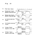
- Fig. 8 illustrates an example wherein the composite video signal used in the NTSC television system is applied to the liquid crystal display device.
- a waveform (a) represents a vertical synchronizing signal
- a waveform (b) represents a horizontal synchronizing signal
- a waveform (c) represents a composite video signal
- a waveform (d) represents sampling pulses.
- Left-hand and right-hand portions of the vertical synchronizing signal (a) correspond respectively to the odd- and even-numbered fields and, at each of the odd- and even-numbered field, the scanning signals are successively outputted in synchronism with the horizontal synchronizing signal (b).
- sampling pulses having the frequency which is determined in dependence on the number of the picture elements in the horizontal direction, that is, the number of the picture element electrodes in the horizontal direction, and video signals for driving the liquid crystal cells are supplied to the respective liquid crystal cells in dependence on the video signals so sampled.
- Fig. 9 illustrates an example wherein the composite video signal used in the NTSC television system is applied to the liquid crystal display device of the present invention.
- a waveform (e) represents a horizontal synchronizing signal during each odd-numbered field;
- a waveform (f) represents first sampling pulses;
- a waveform (g) represents second sampling pulses; and
- a waveform (h) represents a composite video signal.
- the composite synchronizing signal (h) shown in Fig. 9 is identical with the composite synchronizing signal (c) shown in Fig. 8 and is sampled by the first and second sampling pulses (f) and (g), wherein the first sampling pulses (f) are sampling pulses for the first video signal which is applied to the first picture element electrodes 216 to 223 corresponding to the scanning lines 211 and 213 for each odd-numbered row whereas the second sampling pulses (g) are sampling pulses for the second video signal which is applied to the second picture element electrodes 224 to 231 corresponding to the scanning lines 212 and 214 for each even-numbered row.
- the first and second sampling pulses (f) and (g) are displaced a half-cycle period in phase relative to each other such that an intermediate point between points sampled by the first sampling pulses can be sampled by the second sampling pulses.
- the odd-numbered scanning line 211 and the next adjacent even-numbered scanning line 212 are paired for scanning and the subsequent odd-numbered scanning line 213 and the next adjacent even-numbered scanning line 214 are paired for scanning. Accordingly, the composite video signal (h) shown in Fig.
- Fig. 10 illustrates a timing chart showing the operation of the first, second, third and fourth liquid crystal cells 264, 265, 266 and 267 during the interlaced scanning.
- a waveform (i) represents a vertical synchronizing signal during each of the odd- and even-numbered field for he image reproduction having a frequency of 60 Hz wherein one picture, that is, one frame, is comprised of 30 Hz between points 381 and 382.
- Waveforms (j) and (k) represent respective scan synchronizing signals for the scanning lines 211 and 212
- waveforms (1) and (m) represent respective scan synchronizing signals for the scanning lines 213 and 214.
- a waveform (n) represents an example of an analog sample-hold signal corresponding to a video signal voltage supplied to the first liquid crystal cell 264 and outputted from the first video signal supply circuit 209.
- Waveforms (o) to (r) illustrate respective models of analog sample-hold signals similar to the analog sample-hold signal (n), wherein the waveform (o) represents the polarity of the first video signal supplied to the first liquid crystal cell 264; the waveform (p) represents the polarity of the second video signal supplied to the second liquid crystal cell 265; the waveform (q) represents the polarity of the first video signal supplied to the third liquid crystal cell 266; and the waveform (r) represents the polarity of the second video signal supplied to the second liquid crystal cell 267.
- the first and second video signals (o) and (p) are outputted from the first and second video signal supply circuits 209 and 210 in synchronism with the scan synchronizing signals (j) and (b) for the scanning lines 211 and 212, respectively, and, subsequently, the first and second video signals (q) and (r), which are the first and second video signals (o) and (p) having been reversed in polarity, respectively, are outputted from the first and second video signal supply circuits 209 and 210 in synchronism with the scan synchronizing signals (l) and (k) for the scanning lines 213 and 214, respectively.
- the first video signal has a phase displaced 180°, that is, a half-cycle period, relative to the second video signal.
- the row of the first picture element electrodes corresponding to the first liquid crystal cell 264 is in the same polarity as the row of the second picture element electrodes corresponding to the second liquid crystal cell 265, and the row of the first picture element electrodes corresponding to the third liquid crystal cell 266 is in the same polarity as the row of the fourth picture element electrodes corresponding to the fourth liquid crystal cell 267.
- the second preferred embodiment of the present invention is effective to provide the liquid crystal display device which does not require the use of the memory of relatively large memory capacity and of the high speed clock frequency and which is substantially free from any possible reduction in resolution and also any possible occurrence of flickers.
- FIG. 11 to 15 illustrate a third preferred embodiment of the present invention, reference to which will now be made.
- reference numerals 301 and 303 represent respective first video signal lines; reference numerals 202 and 204 represent respective second video signal lines; reference numeral 205 represents a first video signal supply circuit; reference numeral 206 represents a second video signal supply circuit; reference numerals 307 to 310 represent respective scanning lines; and reference numeral 311 represents a scanning signal supply circuit.
- Reference numerals 312 to 319 represent respective first picture element electrodes to which the first video signals are applied, respectively; reference numerals 328 to 335 represent second picture element electrodes to which the second video signals are applied, respectively; and reference numerals 320 to 327 represent respective thin film transistors connected to the first video signal lines 301 and 303, and reference numerals 336 to 343 represent respective thin film transistors connected to the second video signal lines 302 and 304.
- Reference numerals 344 to 351 represent counter electrodes disposed in face-to-face relationship with the first picture element electrodes 312 to 319, respectively; reference numerals 352 to 359 represent counter electrodes disposed in face-to-face relationship with the second picture element electrodes 328 to 335 and 224 to 231; reference numeral 360 represents a first counter electrode signal supply circuit; reference numeral 361 represents a second counter electrode signal supply circuit; and reference numerals 362, 363, 364 and 365 represent respective first, second, third and fourth liquid crystal cells corresponding to the first picture element electrode 313, the second picture element electrode 328, the first picture element electrode 313 and the second picture element electrode 329.
- the first video signals from the first video signal supply circuit 305 are supplied to the first picture element electrodes 312 to 319 through the thin film transistors 320 to 327, respectively, whereas the second video signals from the second video signal supply circuit 206 are supplied to the second picture element electrodes 328 to 335 through the thin film transistors 336 to 343, respectively.
- the sequence of scanning is such that, at each odd-numbered field, the scanning signals are outputted from the scanning signal supply circuit 311 to the odd-numbered scanning lines 307 and 309 to cause respective gates of the thin film transistors 320, 336, 324 and 340 to conduct to apply the first video signals to the first picture element electrodes 312 and 316 and the second video signals to the second picture element electrodes 328 and 332, followed by conduction of respective gates of the thin film transistors 322, 338, 326 and 342 to apply the first video signals to the first picture element electrodes 314 and 318 and the second video signals to the second picture element electrodes 330 and 334.
- the scanning signals are outputted from the scanning signal supply circuit 311 to the even-numbered scanning lines 308 and 310 to cause respective gates of the thin film transistors 321, 337, 325 and 341 to conduct to apply the first video signals to the first picture element electrodes 313 and 317 and the second video signals to the second picture element electrodes 329 and 333, followed by conduction of the respective gates of the thin film transistors 323, 339, 327 and 343 to apply the first video signals to the first picture element electrodes 315 and 319 and the second video signals to the second picture element electrodes 331 and 335.
- Fig. 12 illustrates a timing chart showing the operation of the first, second, third and fourth liquid crystal cells during the interlaced scanning.
- a waveform (A) represents a vertical synchronizing signal during each of the odd- and even-numbered field for he image reproduction having a frequency of 60 Hz wherein one picture, that is, one frame, is comprised of 30 Hz between points 381 and 382.
- Waveforms (B) and (C) represent respective scan synchronizing signals for the scanning lines 307 and 309 at the odd-numbered fields
- waveforms (D) and (E) represent respective scan synchronizing signals for the scanning lines 308 and 310 at the even-numbered fields.
- a waveform (F) represents an analog sample-hold signal corresponding to a video signal voltage supplied to the first picture element electrode 312 and outputted from the first video signal supply circuit 305, the value of which varies between voltages V1 and V2.
- Waveforms (G) to (J) illustrate respective models of analog sample-hold signals similar to the analog sample-hold signal (F), representing the polarities of the first and second video signals supplied to the first and second picture element electrodes 312, 313 and 328, 329, wherein the waveform (G) represents the polarity of the first liquid crystal cell 362, the waveform (H) represents the polarity of the second liquid crystal cell 363, the waveform (I) represents the polarity of the third liquid crystal cell 364 and the waveform (J) represents the polarity of the fourth liquid crystal cell 364.
- Waveforms (K) to (N) represent light responses of the first to fourth liquid crystal cells 362, 363, 364 and 365 corresponding to the signals (G) to (J), respectively.
- the first and second video signals (G) and (H) are outputted from the first and second video signal supply circuits 305 and 306 in synchronism with the scan synchronizing signals (B) on the scanning lines 307, respectively, and, subsequently, during each even-numbered field, the first and second video signals (I) and (J), which are delayed 90° in phase, that is, 1/4 cycle, relative to the similar signals during the odd-numbered field, are outputted from the first and second video signal supply circuits 305 and 306 in synchronism with the scan synchronizing signals (D) on the scanning lines 213 and 214, respectively.
- the signal (H) of drive polarity for the second liquid crystal cell 363 has a phase displaced 180°, that is, a half-cycle period, relative to the signal (G) of drive polarity for the adjacent first liquid crystal cell 362.
- the signal (J) of drive polarity for the fourth liquid crystal cell 365 has a phase displaced 180°, that is, a half-cycle period, relative to the signal (I) of drive polarity for the third liquid crystal cell 364.
- a waveform (O) represents a composite light response formed by combining the light responses (K) to (N), and, when the first to fourth liquid crystal cells 362 to 365 are considered as forming a single block, the light response will be 60 Hz, illustrating that the occurrence of the flicker can be eliminated by this method.
- Fig. 13 illustrates a graph showing one example of the relationship between the light transmission and the applied voltage (effective value) of the liquid crystal cell having a normal white characteristic used in the illustrated embodiment.
- R, G and B indicate a difference in wavelength, wherein R represents a red light (632 nm), G represents a green light (520 nm) and B represents a blue light (488 nm).
- the light transmission of the liquid crystal cell is high, when the applied voltage V is zero, resulting in a bright color display. If the applied voltage V is increased, the light transmission starts decreasing at a threshold voltage value Va and attains a minimum value when the applied voltage attains a value Vb, resulting in a dark color display.
- Fig. 14 is a timing chart showing the voltage signals applied to the neighboring first and second liquid crystal cells 362 and 362 when a dark color display is desired with the use of the liquid crystal cell having a normal white characteristic, wherein in order to apply the voltage corresponding to a threshold value to these liquid crystal cells first and second counter electrode signals are respectively applied to the first and second counter electrodes 344 and 352.
- a waveform (P) represents an odd- or even-numbered field synchronizing signal for the picture display which is similar to the signal (A) shown in Fig. 12.
- a waveform (Q) represents a signal identical with the signal (F) shown in Fig. 12, i.e., analog sample-hold signal corresponding to the video signal voltage supplied to the first picture element electrode 312 and outputted from the first video signal supply circuit 305, the voltage of which varies between values V1 and V2.
- a waveform (R) represents an analog sample-hold signal supplied to the second picture element electrode 328 and outputted from the second video signal supply circuit 306, said signal (R) having a phase displaced a half-cycle period relative to the signal (Q).
- Waveforms (S) and (T) represent a bias voltage of the first counter electrode signal supplied to the first counter electrode 344 and a bias voltage of the second counter electrode signal supplied to the second counter electrode 352, respectively, the value of each of which varies between a low level of a voltage V3 and a high level of a voltage V4.
- the signal (T) has a phase displaced a half-cycle period relative to the signal (S).
- Waveforms (U) and (V) represent signals of applied voltages applied to the first and second liquid crystal cells 362 and 363, respectively.
- the scanning line 307 is scanned and, when the respective gates of the thin film transistors 320 and 336 are brought into conductive state, the signals (Q) and (R) are supplied through the first and second video signal lines 301 and 302, respectively.
- the signals (S) and (T) which are the bias voltages are applied to the first and second counter electrodes 344 and 352, respectively, the signal (U) of the voltage applied to the first liquid crystal cell 362 becomes the difference between the signal (Q) and the signal (S) while the signal (V) of the voltage applied to the second liquid crystal cell 363 will become the difference between the signal (R) and the signal (T) and, as a result thereof, the signals (U) and (V) are respectively applied to the first and second liquid crystal cells 362 and 363, varying in amplitude between the maximum value (V1 - V3) and the minimum value (V2 - V4). Also, the signal (V) of the voltage applied to the second liquid crystal cell 363 has a phase displaced a half-cycle period relative to the signal (U) of the voltage applied to the adjacent first liquid crystal cell 362.
- Fig. 15 is a timing chart similar to Fig. 14, which is applicable when a bright color display is desired with the use of the liquid crystal cell having a normal white characteristic.
- a waveform (1) is similar to the waveform (P) in Fig. 14 and represents an odd- or even-numbered field synchronizing signal for the picture display.
- a waveform (2) is similar to a waveform (Q) in Fig. 14 and represents an analog sample-hold signal corresponding to the video signal voltage supplied to the first picture element electrode 312 and outputted from the first video signal supply circuit 5, the voltage of which varies between values V5 and V6 for the bright color display.
- a waveform (3) represents an analog sample-hold signal supplied to the second picture element electrode 328 and outputted from the second video signal supply circuit 306, said signal (3) having a phase displaced a half-cycle period relative to the signal (2).
- Waveforms (4) and (5) represent a bias voltage of the first counter electrode signal supplied to the first counter electrode and a bias voltage of the second counter electrode signal supplied to the second counter electrode, respectively, which signals are identical with the signals (S) and (T) shown in Fig. 14.
- Waveforms (6) and (7) represent signals of applied voltages applied to the first and second liquid crystal cells 362 and 363, respectively.
- the signal supply system is identical with that shown in Fig. 14 and, since the bias voltage signals (4) and (50 are supplied to the first and second counter electrodes 344 and 352, respectively, the signal (6) of the voltage applied to the first liquid crystal cell 362 is equal to the difference between the signal (2) and the signal (4) whereas the signal (7) of the voltage applied to the second liquid crystal cell 363 is equal to the difference between the signal (3) and the signal (5) wherefore the signals (6) and (7) are applied to the first and second liquid crystal cells 362 and 363, respectively, with the consequence that the amplitude thereof varies between (V5 - V3) to (V6 - V4).
- the signal (7) of the voltage applied to the second liquid crystal cell 362 has a phase displaced a half-cycle period relative to the signal (6) of the voltage applied to the adjacent liquid crystal cell 362.
- the neighboring liquid crystal cell rows can be driven by the application of the voltages displaced a half-cycle period in phase from each other.
- the applied voltage V of the video signal such as shown in Fig. 13 can be oscillated between the voltage value Va and the voltage value Vb with the consequence that the applied voltage V can approach the voltage value Vb satisfactorily, thereby to accomplish a high contrast picture reproduction without flickers being accompanied.
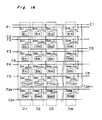
- FIG. 16 to 18 illustrate a fourth preferred embodiment of the present invention, reference to which will now be made.
- Q11, Q12, ⁇ Q2NM represent respective TFTs having their gates connected with gate bus electrodes F1, F2, ⁇ FNM.
- gate bus electrode F1, F2, ⁇ FNM For each gate bus electrode F1, F2, ⁇ FNM, a pair of common line electrodes is provided. So far illustrated, the odd-numbered common line electrodes C1, C3, ⁇ C2N-1 and the even-numbered common line electrodes C2, C4, ⁇ C2N are classified as different groups. While the common line electrodes of each group are connected together and are applied with an identical voltage, the voltage applied to one group of the common line electrodes has a polarity opposite to that of the voltage applied to the other group of the common line electrodes.
- Ones of source and drain electrodes of TFTs in each row are connected to picture element electrodes B11, B12, ⁇ B2NM whereas the others of the source and drain electrodes of TFTs in each row are alternately connected to the paired common line electrodes C1 and C2, C3 and C4, ⁇ C2N-1 and C2n which are positioned on respective sides of the gate bus electrodes F1, F2, ⁇ F2N.
- the TFTs T11, T12, ⁇ T2NM, the gate bus electrodes F1, F2, ⁇ F2N, the common line electrodes C1, C2, ⁇ C2N and the picture element electrodes B11, B12, ⁇ B2NM are all formed on an insulating substrate, for example, a glass plate, and data bus electrodes D1, D2, ⁇ DM which serve as respective counter electrodes as indicated by phantom lines in Fig. 16 are formed on an inner surface of another insulating substrate positioned in face-to-face relationship with such insulating substrate with a liquid crystal layer (not shown) intervening therebetween.
- a voltage applied to the data bus electivelyrodes alternates in polarity in such a manner that the voltage can assumes a positive polarity when applied to the odd-numbered data bus electrodes Dl, D3 and so on while it can assume a negative polarity when applied to the even-numbered data bus electrodes D2, D4 and so on.
- This alternation of the voltage takes place for each frame as is the case with the reversion of the voltage applied to the common line electrodes.
- the electrodes of the TFTs T11, T12, ⁇ T2NM which are connected to the picture element electrodes B11, B12, ⁇ B2NM may be either drains or sources thereof, and similarly, the electrodes which are connected to the common line electrodes may be either sources or drains.
- a data signal voltage is, during the interlaced scanning, sequentially written in first, third, ⁇ 2N-1th rows of liquid crystal cells each formed by the associated picture element electrode B11, B12, ⁇ B2NM, the associated data bus electrode D1, D2, ⁇ DM and the liquid crystal layer, and then in second, fourth, ⁇ 2Nth rows of the liquid crystal cells.
- the scanning signal is sequentially applied to the first, third, ⁇ 2N-1th rows and, at the same time, positive and negative bias voltages are alternately applied to the odd- and even-numbered common line electrodes C1, C2, C3, C4, ⁇ C2N-1 and C2N for one frame (two-field) period and, on the other hand, negative and positive data signal voltages are alternately applied to the odd- and even-numbered data bus electrodes D1, D2, ⁇ DM in an amplitude corresponding to contents to be displayed.
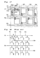
- voltages of polarities such as shown in blocks Ba and Bd in Fig. 18 are applied to the picture element electrodes and the data bus electrodes. It is, however, to be noted that in Fig. 18 only picture elements in the first to fourth column for the first to fourth rows are illustrated.
- the scanning signal is sequentially applied to the second, fourth, ⁇ 2Nth rows and, at the same time, positive and negative bias voltages are alternately applied to the odd- and even-numbered common line electrodes and, on the other hand, positive and negative data signal voltages are alternately applied to the odd- and even-numbered data bus electrodes in an amplitude corresponding to contents to be displayed. Therefore, voltages of polarities such as shown in blocks Bf and Bh in Fig. 18 are applied to the picture element electrodes and the data bus electrodes. At this time, blocks Be and Bg in Fig. 18 indicate that what has been written during the previous field (the first field) is retained without being changed.
- the scanning signal is sequentially applied to the first, third, ⁇ 2N-1th rows and, at the same time, negative and positive bias voltages are alternately applied to the odd- and even-numbered common line electrodes for each frame (two-field) period and, on the other hand, positive and negative data signal voltages are alternately applied to the odd- and even-numbered data bus electrodes in an amplitude corresponding to contents to be displayed. Therefore, voltages of polarities such as shown in blocks Bj and B1 in Fig. 18 are applied to the picture element electrodes and the data bus electrodes. At this time, blocks Bj and B1 in Fig. 18 indicate that what has been written during the previous field (the second field) is retained without being changed.
- the scanning signal is sequentially applied to the second, fourth, ⁇ 2Nth rows and, at the same time, positive and negative bias voltages are alternately applied to the odd- and even-numbered common line electrodes and, on the other hand, negative and positive data signal voltages are alternately applied to the odd- and even-numbered data bus electrodes in an amplitude corresponding to contents to be displayed. Therefore, voltages of polarities such as shown in blocks Bn and Bp in Fig. 18 are applied to the picture element electrodes and the data bus electrodes. At this time, blocks Bm and Bo in Fig. 18 indicate that what has been written during the previous field (the first field) is retained without being changed.
- the voltage of the polarity identical with that during the first field F1 is applied to the picture element electrodes and the data bus electrodes in the same manner, thereby repeating the above cycle. It is to be noted that the sum of data signal voltage corresponding to the contents to be displayed and the bias voltages which have been applied to the common line electrodes is retained for one frame (two-field) period after having been written in the above mentioned liquid crystal cells, but the contents which have been so written will not vary notwithstanding change in potential resulting from the data signal of the data bus electrodes or change in bias voltages applied to the common line electrodes, so long as the TFTs are switched off.
- a pattern 410 of gate electrodes made of Cr, 2,000 angstroms in thickness is first formed on an insulating substrate made of, for example, a glass plate, and an insulating film 420, 3,000 angstroms in thickness, of, for example, silicon nitride is subsequently formed over the gate electrode pattern by the use of a CVD technique.
- an amorphous silicon film 440 500 angstroms in thickness, is deposited over the insulating film 420, followed by etching to provide amorphous silicon islands 440 which are in turn deposited with phosphorus doped amorphous silicon n+ to a thickness of 2,000 angstroms by the use of a CVD technique.
- the resultant film of titanium is etched to form a pattern of common line electrodes 450 and a drain pad 460.
- a layer of n+ is etched on the same pattern to form a drain contact 465 and a source contact 455 relative to the amorphous silicon islands 440, thereby completing the TFTs, the gate bus electrodes and the common line electrodes.
- the substrate as a whole is deposited with an insulating film 425 of silicon nitride by the use of a plasma CVD technique to a thickness of 3,000 angstroms to form electrode lead-out portions and contact holes 470.
- ITO is deposited to a thickness of 2,000 angstroms and is then etched to complete the picture element electrodes 430.
- this substrate is formed with a polyimide film as a liquid crystal molecular orientation film and, after this substrate and an insulating substrate formed by ITO with stripes of counter electrodes (data bus electrodes) D1, D2, ⁇ and a polyimide film have been subjected to an orienting process by means of rubbing, the both are pasted together with a liquid crystal subsequently injected, thereby to complete the liquid crystal display device of the present invention.
- the active matrix liquid crystal display device is effective to substantially eliminate the occurrence of flickers even when a televised picture is scanned according to the interlaced scanning system when driven by an alternating voltage. Moreover, since the voltage applied to t he common line electrodes acts as a bias voltage, a high contrast ratio can be obtained even with a relatively small data signal voltage. Also, a margin relative to any possible variation in output characteristic of a data driver can be increased. Furthermore, since there is no line which would intersect the gate bus electrodes, any possible line defect which would occur when there is a line intersecting the gate bus electrodes will not occur.
Abstract
Description
- The present invention generally relates to liquid crystal display devices and, more particularly, to a liquid crystal display device adapted to be driven by a television signal.
- Fig. 19 of the accompanying drawings illustrates, in the form of an equivalent circuit, the typical prior art liquid crystal display device. Reference to Fig. 19 will now be made for the purpose of discussion of the prior art which is believed to be pertinent to the present invention.
- The prior art liquid crystal display device shown in Fig. 19 comprises a plurality of
liquid crystal cells 1, each shown in the form of an equivalent capacitor,display electrodes 2 thereof and matingcounter electrodes 3. Athin film transistor 4 of MIS structure is connected to eachliquid crystal cell 1 as a switching active element for driving the respectiveliquid crystal cell 1. In practice, theliquid crystal cells 1 and thethin film transistors 4 are arranged in a matrix having a plurality of, for example, four, rows of source lines S1, S2, S3 and S4 and a plurality of, for example, four, columns of control lines G1, G2, G3 and G4, only a portion of which is shown in Fig. 19. As shown, thetransistors 4 in each of the first to fourth rows have their gates connected to the associated control line G1, G2, G3 or G4. The first to fourth control lines are adapted to be scanned according to an interlaced scanning scheme so that the first and third control lines G1 and G3 can be excited by odd-numbered line scanning of the television signal whereas the second and fourth control lines G2 and G4 can be excited by even-numbered line scanning of the same television signal. A predetermined voltage inverted for each frame is applied to the counter electrodes of the respectiveliquid crystal cells 1 as a drive voltage. - Video signals (for example, R, G and B signals) to be displayed are supplied through the source lines S1 to S4.
- During the odd-numbered field of the television signal, the first and third control lines are successively excited by a scanning signal (line sequence pulses conforming to a horizontal synchronizing signal) so that a video signal voltage can be sequentially applied to the liquid crystal cells in the first row and the liquid crystal cells in the third row. At this time, the transistors in each of the second and fourth rows are switched off.
- During the even-numbered field of the television signal, the second and fourth rows are sequentially scanned with the consequence that the video signal is applied to the liquid crystal cells in the second and fourth rows. At this time, the transistors in each of the first and third rows are switched off and the signal at the odd-numbered field is remains retained.
- During the subsequent frame, the polarity of the voltage applied between the
electrodes liquid crystal cells 1 are reversed. In such case, the liquid crystal drive frequency will be 15 Hz if the television signal according to NTSC system is used to drive the liquid crystal cells. This is partly because the television signal is based on the interlaced scanning scheme in which the odd-numbered and even-numbered horizontal lines of the screen are scanned for each different field and partly because the electric field applied to theliquid crystal cells 1 is required to be cyclically reversed in view of the lifetime. Considering one picture element for facilitating a better understanding, the application of a positive voltage between both electrodes of each cell is repeated at intervals of four fields. This is because the picture element referred to above is, after having been scanned at a n-th field, will not be scanned at the next succeeding, (n+1)th field for the purpose of interlacing; will be scanned at the subsequent (n+2)th field while applied with a negative voltage in view of the lifetime of the liquid crystal cells; and will not be scanned at the (n+3)th field for the purpose of interlacing. At the (n+4)th field, the liquid crystal cell of the picture element is again applied with a positive voltage. Thus, the application of the positive voltage to each liquid crystal cell takes place at intervals of the four fields which, in terms of the drive frequency, correspond to 15 Hz according to the NTSC system or 12.5 Hz according to the PAL system. - In the prior art liquid crystal display device of the above discussed construction, in view of the fact that the liquid crystal cells are alternately driven, the liquid crystal drive frequency will become one half the frame frequency, that is, 15 Hz, when display is effected based on the interlaced scanning scheme. While the frequency of 30 Hz will not be perceived as a flicker by human eyes, the frequency of 15 Hz is recognized as a flicker appearing on the screen and, as a result thereof, a picture uncomfortable to look will be reproduced. In order to substantially avoid this problem, a drive method has been suggested wherein a combination of each two of the rows is changed for each field so that every two rows can be simultaneously driven by the same video signal. According to this suggested method, although the drive frequency can be improved to 30 Hz, no improvement has been made in the number of effective display scanning lines per field. Specifically, assuming that the number of the effective display scanning lines driven by the same signal is 480 lines, the number of the effective display scanning lines per field remains 240 lines and, accordingly, the vertical resolution is still insufficient.
- Another method suggested to substantially avoid the above discussed problem is that the use is made of a frame memory so that an image data corresponding to two video signal lines can be displayed during the scanning period of one horizontal scanning line Gi (i=1 to m). However, this method has problems in that the use of a memory having a large memory capacity corresponding to the number of the display liquid crystal cells c is required and that a high speed is required in the clock frequency for a drive driver for driving active elements, resulting in the increased manufacturing cost.
- Accordingly, the present invention has been devised with a view to providing an improved liquid crystal display device effective to substantially eliminating the above discussed problems inherent in the prior art liquid crystal display devices.
- Another important object of the present invention is to provide an improved active matrix type liquid crystal display device of the type referred to above, which is effective to accomplish a reproduction of a picture with no flicker occurring and with no vertical resolution being lowered.
- A further object of the present invention is to provide an improved liquid crystal display device of the type referred to above, which does not require the use of the memory having a large memory capacity and the high speed clock frequency.
- A still further object of the present invention is to provide an improved liquid crystal display device of the type referred to above, wherein a bias voltage is applied to the counter electrodes in correspondence with the polarity of the video signal then reversed for each neighboring liquid crystal cells thereby to accomplish a high-contrast picture reproduction without flicker being accompanied.
- A yet further object of the present invention is to provide an improved liquid crystal display device of the type referred to above, wherein no possible shortcircuiting will occur at each point of intersections of lines and wherein a high contrast ratio can be obtained even though the drive voltage is relatively low.
- In one aspect of the present invention, there is provided an active matrix liquid crystal display device operable on an interlaced scanning scheme and having a plurality of liquid crystal cells and switching active elements for driving the liquid crystal cells, said liquid crystal cells and said switching active elements being arranged in a matrix fashion having rows and columns intersecting with each other, which device comprises a plurality of sets, each comprised of each neighboring members of the rows of the matrix; means for scanning each set with an interlaced scanning signal at any fields, odd-numbered source lines each connected with one of said row forming the respective set, even-numbered source lines each connected with the other of said row forming the respective set; and means for applying an odd-numbered field signal to said odd-numbered source line at any field time and for applying an even-numbered field signal to said even-numbered source line at any field time.
- According to the above described construction, each set of the neighboring rows can be scanned according to the interlaced scanning scheme, and one of the neighboring rows and the other of the neighboring rows are applied with odd- and even-numbered field signals at any field time, respectively. Accordingly, when one picture element is taken into consideration, it can be scanned at any field time and, therefore, the voltages applied to the opposite electrodes of the liquid crystal cells per field can be reversed in polarity. This means that the driving frequency is 30 Hz. Moreover, since the odd- and even-numbered field signals are respectively applied to the respective set of the neighboring rows, 480 scanning lines can be utilized per field if the number of effective display scanning lines is assumed to be 480 lines. Also, the scanning time per row corresponds to one horizontal period and, therefore, no high speed characteristic is required.
- In another aspect of the present invention, there is provided an active matrix liquid crystal display device including a plurality of rows of video signal lines, a plurality of columns of scanning lines, said rows of the video signal line and the columns of the scanning lines being arranged in a matrix fashion, a picture element electrode disposed at each of intersecting points between the rows and the columns and adapted to receive a video signal through an active element, said device being adapted to be scanned according to an interlaced scanning scheme by a signal supplied through the scanning lines, which device comprises said video signal lines being comprised of a plurality of pairs of first video signal lines and a plurality of pairs of second video signal lines; a first video signal supply means for supplying a first video signal to the first video signal lines; a second video signal supply means for supplying a second video signal to the second video signal lines, said second video signal having a phase displaced a half-cycle period relative to the first video signal; a scanning signal supply means for supplying a scanning signal to each of a plurality of sets of odd- and even-numbered scanning lines; and first and second picture element electrodes to which the first and second video signals are respectively applied, said first and second picture element electrodes being arranged displaced a half-cycle period from each other in a direction of the scanning line.
- According to the above described construction, the first and second video signals have their phases displaced a half-cycle period from each other, and the first and second picture element electrodes are arranged while displaced a half-cycle period in a direction conforming to the scanning line so that each neighboring odd- and even-numbered scanning lines can be scanned. Therefore, the televised picture substantially free from the occurrence of flickers can be displayed.
- In a further aspect of the present invention, there is provided an active matrix liquid crystal display device including a plurality of rows of video signal lines, a plurality of columns of scanning lines, said rows of the video signal line and the columns of the scanning lines being arranged in a matrix fashion, a picture element electrode disposed at each of intersecting points between the rows and the columns and adapted to receive a video signal through an active element, said device being adapted to be scanned according to an interlaced scanning scheme by a signal supplied through the scanning lines, which device comprises a scanning signal supply means for supplying a signal to each of the scanning lines; a first video signal supply means for supplying a first video signal to odd-numbered columns of the video signal lines; a second video signal supply means for supplying a second video signal to even-numbered columns of the video signal lines, said second video signal having a phase displaced a half-cycle period relative to the first video signal; first and second picture element electrodes to which the first and second video signals are respectively applied; a first counter electrode confronting each of the first picture element electrodes; a second counter electrode confronting each of the second picture element electrodes; a first counter electrode signal supply means for supplying a first counter electrode signal to the first counter electrodes; and a second counter electrode signal supply means for supplying a second counter electrode signal to the second counter electrodes, said second counter electrode signal having a phase displaced a half-cycle period relative to the first counter electrode signal.
- According to the above described construction, since the first and second video signals have their phases displaced a half-cycle period from each other and the first and second counter electrodes are arranged while displaced a half-cycle period in phase from each other, it is possible to apply a bias voltage to the counter electrodes with respect to the polarity of the video signal which is reversed for each of the odd- and even-numbered lines of the video signal. Therefore, the televised picture can be displayed at a relatively high contrast with no flicker being accompanied.
- In a still further aspect of the present invention, there is provided an active matrix liquid crystal display device which has a first insulating substrate formed with thin film transistors, gate bus electrodes, common line electrodes and picture element electrodes which do not intersect with the gate bus electrodes, a second insulating substrate formed with data bus electrodes so as to confront the first insulating substrate and so as to intersect the gate bus electrodes, and a layer of liquid crystal intervening between the first and second insulating substrates, which device comprises each of said thin film transistors, which are connected to the same gate bus electrodes, having source and drain electrodes, one of said source and drain electrodes being connected with the picture element electrode and the other of said source and drain electrodes being alternately connected with two common line electrodes confronting with each other with the gate electrode intervening therebetween, said two common line electrodes being applied with voltages different in polarity from each other.
- According to the above described construction, each of the thin film transistors in each row is alternately applied with positive and negative voltages supplied through the paired common line electrodes. In correspondence with this, the data bus electrodes which act as counter electrodes are also alternately applied with negative and positive data signal voltages. By way of example, in the case of the television image according to the interlaced scanning scheme, the reversion of the applied voltages to the paired common line electrodes and the reversion of the data signal voltages take place for each field at a frequency of 15 Hz. However, considering the screen as a whole, a combination of the positive and negative polarities varies for each field such that the positive charged picture elements and the negative charged picture elements are equal in number with each other while neighboring with each other, and therefore, the flickering frequency will be apparently 60 Hz enough to substantially eliminate the occurrence of flickers on the televised picture.
-
- These and other objects and features of the present invention will become readily understood from the following description taken in conjunction with preferred embodiments thereof with reference to the accompanying drawings, in which:
- Fig. 1 is an equivalent circuit diagram of a liquid crystal display device according to a first preferred embodiment of the present invention;
- Fig. 2 is a circuit block diagram showing the details of a signal processing unit employed in the liquid crystal display device of Fig. 1;
- Fig. 3 is a chart showing respective waveforms of various signals appearing in the circuit of Fig. 2;
- Fig. 4 is a chart showing respective waveforms of various signals used to drive the liquid crystal display device of Fig. 1;
- Fig. 5 is a schematic diagram showing an arrangement of picture elements corresponding to the arrangement of electrodes in the liquid crystal display device shown in Fig. 1;
- Fig. 6 is an equivalent circuit diagram of a liquid crystal display device of active matrix type according to a second preferred embodiment of the present invention;
- Fig. 7 is a schematic diagram showing an arrangement of picture elements corresponding to the arrangement of electrodes in the liquid crystal display device of Fig. 6;
- Fig. 8 is a chart showing respective waveforms of signals contained in the NTSC television signal which is used in the practice of the liquid crystal display device;
- Fig. 9 is a chart showing respective waveforms of signals contained in the NTSC television signal which is used in the practice of the liquid crystal display device of the present invention;
- Fig. 10 is a timing chart showing the sequence of operation of first to fourth liquid crystal cells during the interlaced scanning in the device of Fig. 6;
- Fig. 11 is an equivalent circuit diagram of a liquid crystal display device of active matrix type according to a third preferred embodiment of the present invention;
- Fig. 12 is a timing chart showing the sequence of operation of first to fourth liquid crystal cells during the interlaced scanning in the device of Fig. 11;
- Fig. 13 is a graph showing the relationship between the light transmission and the voltage applied to liquid crystal cells having a normal white characteristic used in the embodiment of Fig. 11;
- Fig. 14 is a timing chart showing voltage signals applied to the neighboring first and second liquid crystal cells when a dark display is effected with the use of the liquid crystal cells having the normal white characteristic;
- Fig. 15 is a timing chart showing voltage signals applied to the neighboring first and second liquid crystal cells when a bright display is effected with the use of the liquid crystal cells having the normal white characteristic;
- Fig. 16 is an equivalent circuit diagram of a liquid crystal display device of active matrix type according to a fourth preferred embodiment of the present invention;
- Fig. 17 is a schematic diagram used to explain a process of manufacture of the liquid crystal device of Fig. 16;
- Fig. 18 is a chart showing effects derived when a televised image is scanned according to an interlaced scanning scheme by alternating voltage drive in the device according to the fourth embodiment of the present invention; and
- Fig. 19 is an equivalent circuit diagram of the prior art liquid crystal display device.
- Referring first to Figs. 1 and 2, a plurality of liquid crystal cells C11 to C44 and a corresponding number of thin film transistors T11 to T44 are arranged in a matrix form having rows and columns, each neighboring rows being paired to provide a corresponding row line pair A1 and A2, each row line pair A1 and A2 being adapted to be driven by a respective interlaced scanning signal. Accordingly, gate electrodes of the transistors T11 to T14 and T21 to T24 in the first and second rows, respectively, are connected to a first control line G1 and, similarly, gate electrodes of the transistors T31 to T34 and T41 to T44 in the third and fourth rows, respectively, are connected to a second control line G2. Reference numeral 111 represents an odd-numbered source line driver having output signal lines S1, S3, S5 and S7 which are connected to respective source electrodes of the transistors in one of the neighboring rows forming the respective row pair, for example, in the first and third rows.
Reference numeral 112 represents an odd-numbered source line driver having output signal lines S2, S4, S6 and S8 which are connected to respective source electrodes of the transistors in the other of the neighboring rows forming the respective row pair, that is, in the second and fourth rows. - The odd-numbered source line driver 111 is adapted to receive red, green and blue signals Ro, Go and Bo of odd-numbered fields. Since the liquid crystal cells shown in Fig. 1 form each color picture element as shown in Fig. 5, the red signal Ro is outputted through the output lines S1 and S7, the green signal Go is outputted through the output line S3 and the blue signal Bo is outputted through the output line S5. On the other hand, the odd-numbered
source line driver 112 is adapted to receive red, green and blue signals Re, Ge and Be of even-numbered fields and, therefore, the red signal Re, the green signal Ge and the blue signal Be are outputted through the output lines S2 and S8, the output line S4 and the output line S6, respectively. Although not exclusively limited thereto, the associated signals are assumed to be outputted through the output lines S1, S3, S5 and S7 as well as the output lines S2, S4, S6 and S8 on a time series basis. For this reason, each of thesource line drivers 111 and 112 includes shift registers for providing the inputs sequentially to the output lines and also includes a respective inverting means for inverting the input signals for each scanning line as shown by the waveform (d) in Fig. 4. - While the odd-numbered source line driver 111 is inputted at any field time with signals of odd-numbered fields and, similarly, the even-numbered
source line driver 112 is inputted at any field time with signals of even-numbered fields, a circuit necessary to supply the signals to the odd- and even-numberedsource line drivers 111 and 112 are best illustrated in Fig. 2. - In Fig. 2, reference numeral 13 represents a color separator for separating red, green and blue signals VR, VG and VB from a video signal (c) and outputting the red, green and blue signals VR, VG and VB to an analog-to-digital (A/D)
converter 114 operable to convert each of those signals into a digital amount. Digital outputs from the A/D converter 114 are then supplied throughreal time lines 115,first delay lines 116 andsecond delay lines 117. Thereal time lines 115 include a digital-to-analog (D/A)converter 124 for converting the digital amount into an analog amount, a low-pass filter 126 and first andsecond analog gates first analog gate 128 whereas the red, green and blue signals Re, Ge and Be of the even-numbered fields which have been converted into respective analog amounts are supplied to the even-numberedsource line driver 112 through the second analog gate 29. - Each of the first and
second delay lines digital gate field memory digital gate digital gates second delay lines fourth analog gates analog converter 125 and then through alow pass filter 127. Thethird analog gate 130 has a function of providing the odd-numbered source line driver 111 with one-field preceding odd-numbered field signals whereas thefourth analog gate 131 has a function of providing the even-numberedsource line driver 112 with the one-field preceding even-numbered field signals. Since the A/D converter 114 converts each color signal into an 8-bit digital amount, the digital circuit shown in Fig. 2 is effective to perform an 8-bit processing for each color signal. - The
memories memory 120 during the odd-numbered field, thememory 121 reads out the color signal data of the one-field preceding even-numbered fields. Accordingly, at the odd-numbered field, the signal of the odd-numbered field is applied to the odd-numbered source line driver 111 through thereal time lines 115, whereas the one-field preceding even-numbered field signal read out from thememory 121 is supplied to the even-numberedsource line driver 112. At this time, the signal of the odd=numbered field is written in thememory 120. At the subsequent even-numbered field, the signal of the even-numbered field is supplied to the even-numberedsource line driver 112 through thereal time lines 115, whereas the one-field preceding odd-numbered field signal read out from thememory 120 is supplied to the odd-numbered source line driver 111. At this time, the signal of the even-numbered field is written in thememory 121. It is to be noted that, although in Fig. 2 the A/D conversion and the subsequent D/A conversion are successively effected so that, since the first andsecond delay lines real time lines 115 may be equally affected as in the signal processed through the digital circuits, the outputs from thecolor separator 113 may be supplied direct to the first andsecond analog gates memories - Fig. 3 illustrates a chart of respective waveforms of gate signals appearing in the circuit of Fig. 2. In Fig. 3, the waveform (a) represents a vertical synchronizing signal contained in the video signal, wherein ODD and EVEN stand for odd-numbered and even-numbered fields, respectively; the waveform (b) represents a horizontal scanning signal in which equalizing pulses are not shown; the waveform (c) represents the video signal applied to the
color separator 113; and the waveform (d) represents sampling pulses of the A/D converter 114 having a frequency expressed by fs. Each of the D/A converters memory 120 at the odd-numbered field; the waveform (f) represents a write-in signal to be written in thememory 121 at the even-numbered field; the waveform (g) represents a conduction control signal to be applied to thegates gates - While the odd- and even-numbered field color signals are supplied to the odd- and even-numbered
source line drivers 111 and 112, respectively, from the circuit shown in and described with reference to Fig. 2, drive signals for respective circuit components of Fig. 1 are shown in Fig. 4. In Fig. 4, a waveform (a) represents a vertical synchronizing signal; waveforms (b) and (c) represent scanning signals applied respectively to the first and second control lines G1 and G2; and a waveform (d) represents the polarity of the color signals supplied from the odd- and even-numberedsource line drivers 111 and 112 to the respective source electrodes of the transistors through the output lines S1, S3, S5 and S7 and the output lines S2, S4, S6 and S8. Waveforms (e), (f), (g), (h), (i) and (j) represent examples of drive voltages applied to the counter electrode 103 of the liquid crystal cells C11, C21, C31, C12, C22 and C32, respectively, each of said drive voltages being reversed in polarity for each field. Accordingly, the driving frequency is 30 Hz and, hence, no flicker occur. Moreover, since in the illustrated embodiment the video signal (color signals), too, is reversed for each line as shown by the waveform (d) in Fig. 4, the occurrence of the flicker can further be eliminated. Each row line pair A1 or A2 is operated by the normal interlaced scanning signal regardless of the field. This is because the odd-numbered field scanning signal is first applied to the first control line G1 to switch both of the first and second rows on and is then applied to the second control line G2 during the next succeeding scanning to switch both of the third and fourth rows on and because the even-numbered scanning signal is first applied to the first control line G1 to switch both of the second and first rows on and is then applied to the second control line G2 to switch both of the fourth and third rows on. - It is to be noted that the concept of the present invention which has been described as applied to the NTSC system can be equally applicable to the PAL system.
- As hereinbefore fully described, the frequency of 30 Hz can be employed as the drive frequency for the liquid crystal cells and, accordingly, no flicker substantially occur in the picture being reproduced. Also, since at any field each two line rows are simultaneously operated by the odd- and even-numbered field signals, all of the effective scanning lines can be used for each field and, accordingly, the resolution in the vertical direction can be considerably improved. Moreover, the structure may employ the usual interlaced scanning and the usual scanning speed, and no high speed characteristic is required in data transmission.
- An active matrix type liquid crystal display device according to a second preferred embodiment of the present invention will now be described with reference to Figs. 6 to 10.
- Referring first to Fig. 6,
reference numerals reference numerals reference numeral 209 represents a first video signal supply circuit;reference numeral 210 represents a second video signal supply circuit; andreference numeral 215 represents a scanning signal supply circuit.Reference numerals 216 to 223 represent first picture element electrodes to which the first video signals are applied, respectively;reference numerals 224 to 231 represent second picture element electrodes to which, the second video signals are applied, respectively; andreference numerals 232 to 247 represent respective thin film transistors. - Reference numerals 148 to 163 represent counter electrodes disposed in face-to-face relationship with the first and second
picture element electrodes 216 to 223 and 224 to 231, all of said counter electrodes being connected together.Reference numerals picture element electrodes reference numerals picture element electrodes - The first video signals from the first video
signal supply circuit 209 are supplied to the firstpicture element electrodes 216 to 219 through thethin film transistors 232 to 235, respectively, and also to the firstpicture element electrodes 220 to 223 through thethin film transistors 240 to 243, respectively, whereas the second video signals from the second videosignal supply circuit 210 are supplied to the secondpicture element electrodes 224 to 227 through thethin film transistors 236 to 239, respectively, and also to the secondpicture element electrodes 228 to 231 through thethin film transistors 244 to 247, respectively. - While the interlaced scanning is effected in order to display a picture, the sequence of scanning is such that, at each odd-numbered field, the scanning signals are outputted from the scanning
signal supply circuit 215 to thescanning lines thin film transistors 232 to 239 to conduct to apply the first video signals to the firstpicture element electrodes 216 to 219 and the second video signals to the secondpicture element electrodes 224 to 227, and the scanning signals are subsequently outputted from the scanningsignal supply circuit 215 to thescanning lines thin film transistors 240 to 247 to conduct to apply the first video signals to the firstpicture element electrodes 220 to 223 and the second video signals to the secondpicture element electrodes 228 to 231. Thereafter, the scanning takes place in a manner similar to that described above. At the subsequent even-numbered field, however, the first and second video signals are supplied to the first and secondpicture element electrodes 216 to 231 in a manner similar to the first video signals as hereinabove described, thereby completing the scanning at the odd- and even-numbered fields. - Fig. 7 illustrates the picture element electrodes arranged in correspondence with the arrangement of the picture elements.
- In Fig. 7, reference characters R, G and B represents the three additive primary colors, that is, red, green and blue, wherein the picture elements in each odd-numbered line are displaced a half-cycle period (1/2 pitch) relative to the picture elements in each even-numbered line.
- Fig. 8 illustrates an example wherein the composite video signal used in the NTSC television system is applied to the liquid crystal display device. In Fig. 8, a waveform (a) represents a vertical synchronizing signal; a waveform (b) represents a horizontal synchronizing signal; a waveform (c) represents a composite video signal; and a waveform (d) represents sampling pulses. Left-hand and right-hand portions of the vertical synchronizing signal (a) correspond respectively to the odd- and even-numbered fields and, at each of the odd- and even-numbered field, the scanning signals are successively outputted in synchronism with the horizontal synchronizing signal (b). Sampling pulses (d) shown in Fig. 8 are a signal used to determine how often the composite video signal should be sampled during each horizontal scanning period, said sampling pulses having the frequency which is determined in dependence on the number of the picture elements in the horizontal direction, that is, the number of the picture element electrodes in the horizontal direction, and video signals for driving the liquid crystal cells are supplied to the respective liquid crystal cells in dependence on the video signals so sampled.
- Fig. 9 illustrates an example wherein the composite video signal used in the NTSC television system is applied to the liquid crystal display device of the present invention. In Fig. 9, a waveform (e) represents a horizontal synchronizing signal during each odd-numbered field; a waveform (f) represents first sampling pulses; a waveform (g) represents second sampling pulses; and a waveform (h) represents a composite video signal.
- The composite synchronizing signal (h) shown in Fig. 9 is identical with the composite synchronizing signal (c) shown in Fig. 8 and is sampled by the first and second sampling pulses (f) and (g), wherein the first sampling pulses (f) are sampling pulses for the first video signal which is applied to the first
picture element electrodes 216 to 223 corresponding to thescanning lines picture element electrodes 224 to 231 corresponding to thescanning lines - While in the usual line interlaced scanning the
scanning lines scanning lines scanning line 211 and the next adjacent even-numberedscanning line 212 are paired for scanning and the subsequent odd-numberedscanning line 213 and the next adjacent even-numberedscanning line 214 are paired for scanning. Accordingly, the composite video signal (h) shown in Fig. 9 is the one for the odd-numbered field and, although it does not contain the signal for the even-numbered field, the intermediate point between the points for the odd-numbered fields which have been sampled are compensated for by an interpolation method so that the second video signal can be obtained by sampling the intermediate point. - Fig. 10 illustrates a timing chart showing the operation of the first, second, third and fourth
liquid crystal cells - A waveform (i) represents a vertical synchronizing signal during each of the odd- and even-numbered field for he image reproduction having a frequency of 60 Hz wherein one picture, that is, one frame, is comprised of 30 Hz between
points - Waveforms (j) and (k) represent respective scan synchronizing signals for the
scanning lines scanning lines - A waveform (n) represents an example of an analog sample-hold signal corresponding to a video signal voltage supplied to the first
liquid crystal cell 264 and outputted from the first videosignal supply circuit 209. - Waveforms (o) to (r) illustrate respective models of analog sample-hold signals similar to the analog sample-hold signal (n), wherein the waveform (o) represents the polarity of the first video signal supplied to the first
liquid crystal cell 264; the waveform (p) represents the polarity of the second video signal supplied to the secondliquid crystal cell 265; the waveform (q) represents the polarity of the first video signal supplied to the thirdliquid crystal cell 266; and the waveform (r) represents the polarity of the second video signal supplied to the secondliquid crystal cell 267. - As shown in Fig. 10, during each of the odd- and even-numbered fields, the first and second video signals (o) and (p) are outputted from the first and second video
signal supply circuits scanning lines signal supply circuits scanning lines - At this time, the first video signal has a phase displaced 180°, that is, a half-cycle period, relative to the second video signal.
- Although in Fig. 10 only the first, second, third and fourth
liquid crystal cells liquid crystal cell 264 is in the same polarity as the row of the second picture element electrodes corresponding to the secondliquid crystal cell 265, and the row of the first picture element electrodes corresponding to the thirdliquid crystal cell 266 is in the same polarity as the row of the fourth picture element electrodes corresponding to the fourthliquid crystal cell 267. - Accordingly, since the difference between the analog data signals of the neighboring odd- and even-numbered fields is small and since the arrangement of the picture element electrodes is such that the first picture element electrodes are displaced a half-cycle period from the second picture element electrodes in a direction conforming to the scanning direction, a spectrum of an average light response of a liquid crystal panel will become half the field frequency, that is, 30 Hz and, accordingly, not only will any possible reduction of the resolution be avoided, but also no use of the memory of relatively large memory capacity and the high speed clock frequency is required. Therefore, a picture with no flicker can be reproduced.
- Even the embodiment shown in and described with reference to Figs. 6 to 10 can be equally applicable not only to the NTSC television system, but also to the PAL television system wherein the frequency of 50 Hz is used.
- As hereinbefore described, the second preferred embodiment of the present invention is effective to provide the liquid crystal display device which does not require the use of the memory of relatively large memory capacity and of the high speed clock frequency and which is substantially free from any possible reduction in resolution and also any possible occurrence of flickers.
- Figs. 11 to 15 illustrate a third preferred embodiment of the present invention, reference to which will now be made.
- In Fig. 11,
reference numerals reference numerals reference numeral 205 represents a first video signal supply circuit;reference numeral 206 represents a second video signal supply circuit;reference numerals 307 to 310 represent respective scanning lines; andreference numeral 311 represents a scanning signal supply circuit.Reference numerals 312 to 319 represent respective first picture element electrodes to which the first video signals are applied, respectively;reference numerals 328 to 335 represent second picture element electrodes to which the second video signals are applied, respectively; and reference numerals 320 to 327 represent respective thin film transistors connected to the firstvideo signal lines reference numerals 336 to 343 represent respective thin film transistors connected to the secondvideo signal lines -
Reference numerals 344 to 351 represent counter electrodes disposed in face-to-face relationship with the firstpicture element electrodes 312 to 319, respectively;reference numerals 352 to 359 represent counter electrodes disposed in face-to-face relationship with the secondpicture element electrodes 328 to 335 and 224 to 231;reference numeral 360 represents a first counter electrode signal supply circuit;reference numeral 361 represents a second counter electrode signal supply circuit; andreference numerals picture element electrode 328, the first picture element electrode 313 and the secondpicture element electrode 329. - The first video signals from the first video
signal supply circuit 305 are supplied to the firstpicture element electrodes 312 to 319 through the thin film transistors 320 to 327, respectively, whereas the second video signals from the second videosignal supply circuit 206 are supplied to the secondpicture element electrodes 328 to 335 through thethin film transistors 336 to 343, respectively. While the interlaced scanning is effected in order to display a picture, the sequence of scanning is such that, at each odd-numbered field, the scanning signals are outputted from the scanningsignal supply circuit 311 to the odd-numberedscanning lines thin film transistors picture element electrodes picture element electrodes picture element electrodes picture element electrodes signal supply circuit 311 to the even-numberedscanning lines thin film transistors 321, 337, 325 and 341 to conduct to apply the first video signals to the firstpicture element electrodes 313 and 317 and the second video signals to the secondpicture element electrodes thin film transistors picture element electrodes picture element electrodes - Fig. 12 illustrates a timing chart showing the operation of the first, second, third and fourth liquid crystal cells during the interlaced scanning.
- A waveform (A) represents a vertical synchronizing signal during each of the odd- and even-numbered field for he image reproduction having a frequency of 60 Hz wherein one picture, that is, one frame, is comprised of 30 Hz between
points scanning lines scanning lines picture element electrode 312 and outputted from the first videosignal supply circuit 305, the value of which varies between voltages V1 and V2. - Waveforms (G) to (J) illustrate respective models of analog sample-hold signals similar to the analog sample-hold signal (F), representing the polarities of the first and second video signals supplied to the first and second
picture element electrodes liquid crystal cell 362, the waveform (H) represents the polarity of the secondliquid crystal cell 363, the waveform (I) represents the polarity of the thirdliquid crystal cell 364 and the waveform (J) represents the polarity of the fourthliquid crystal cell 364. - Waveforms (K) to (N) represent light responses of the first to fourth
liquid crystal cells - As shown in Fig. 12, during each odd-numbered field, the first and second video signals (G) and (H) are outputted from the first and second video
signal supply circuits scanning lines 307, respectively, and, subsequently, during each even-numbered field, the first and second video signals (I) and (J), which are delayed 90° in phase, that is, 1/4 cycle, relative to the similar signals during the odd-numbered field, are outputted from the first and second videosignal supply circuits scanning lines liquid crystal cell 363 has a phase displaced 180°, that is, a half-cycle period, relative to the signal (G) of drive polarity for the adjacent firstliquid crystal cell 362. Similarly, the signal (J) of drive polarity for the fourthliquid crystal cell 365 has a phase displaced 180°, that is, a half-cycle period, relative to the signal (I) of drive polarity for the thirdliquid crystal cell 364. A waveform (O) represents a composite light response formed by combining the light responses (K) to (N), and, when the first to fourthliquid crystal cells 362 to 365 are considered as forming a single block, the light response will be 60 Hz, illustrating that the occurrence of the flicker can be eliminated by this method. - Fig. 13 illustrates a graph showing one example of the relationship between the light transmission and the applied voltage (effective value) of the liquid crystal cell having a normal white characteristic used in the illustrated embodiment.
- In Fig. 13, R, G and B indicate a difference in wavelength, wherein R represents a red light (632 nm), G represents a green light (520 nm) and B represents a blue light (488 nm). The light transmission of the liquid crystal cell is high, when the applied voltage V is zero, resulting in a bright color display. If the applied voltage V is increased, the light transmission starts decreasing at a threshold voltage value Va and attains a minimum value when the applied voltage attains a value Vb, resulting in a dark color display.
- Fig. 14 is a timing chart showing the voltage signals applied to the neighboring first and second
liquid crystal cells second counter electrodes - In Fig. 14, a waveform (P) represents an odd- or even-numbered field synchronizing signal for the picture display which is similar to the signal (A) shown in Fig. 12. A waveform (Q) represents a signal identical with the signal (F) shown in Fig. 12, i.e., analog sample-hold signal corresponding to the video signal voltage supplied to the first
picture element electrode 312 and outputted from the first videosignal supply circuit 305, the voltage of which varies between values V1 and V2. A waveform (R) represents an analog sample-hold signal supplied to the secondpicture element electrode 328 and outputted from the second videosignal supply circuit 306, said signal (R) having a phase displaced a half-cycle period relative to the signal (Q). Waveforms (S) and (T) represent a bias voltage of the first counter electrode signal supplied to thefirst counter electrode 344 and a bias voltage of the second counter electrode signal supplied to thesecond counter electrode 352, respectively, the value of each of which varies between a low level of a voltage V3 and a high level of a voltage V4. The signal (T) has a phase displaced a half-cycle period relative to the signal (S). Waveforms (U) and (V) represent signals of applied voltages applied to the first and secondliquid crystal cells - In the neighboring first and second
liquid crystal cells scanning line 307 is scanned and, when the respective gates of thethin film transistors 320 and 336 are brought into conductive state, the signals (Q) and (R) are supplied through the first and secondvideo signal lines second counter electrodes liquid crystal cell 362 becomes the difference between the signal (Q) and the signal (S) while the signal (V) of the voltage applied to the secondliquid crystal cell 363 will become the difference between the signal (R) and the signal (T) and, as a result thereof, the signals (U) and (V) are respectively applied to the first and secondliquid crystal cells liquid crystal cell 363 has a phase displaced a half-cycle period relative to the signal (U) of the voltage applied to the adjacent firstliquid crystal cell 362. - Fig. 15 is a timing chart similar to Fig. 14, which is applicable when a bright color display is desired with the use of the liquid crystal cell having a normal white characteristic.
- Referring to Fig. 15, a waveform (1) is similar to the waveform (P) in Fig. 14 and represents an odd- or even-numbered field synchronizing signal for the picture display. A waveform (2) is similar to a waveform (Q) in Fig. 14 and represents an analog sample-hold signal corresponding to the video signal voltage supplied to the first
picture element electrode 312 and outputted from the first videosignal supply circuit 5, the voltage of which varies between values V5 and V6 for the bright color display. A waveform (3) represents an analog sample-hold signal supplied to the secondpicture element electrode 328 and outputted from the second videosignal supply circuit 306, said signal (3) having a phase displaced a half-cycle period relative to the signal (2). Waveforms (4) and (5) represent a bias voltage of the first counter electrode signal supplied to the first counter electrode and a bias voltage of the second counter electrode signal supplied to the second counter electrode, respectively, which signals are identical with the signals (S) and (T) shown in Fig. 14. Waveforms (6) and (7) represent signals of applied voltages applied to the first and secondliquid crystal cells - The signal supply system is identical with that shown in Fig. 14 and, since the bias voltage signals (4) and (50 are supplied to the first and
second counter electrodes liquid crystal cell 362 is equal to the difference between the signal (2) and the signal (4) whereas the signal (7) of the voltage applied to the secondliquid crystal cell 363 is equal to the difference between the signal (3) and the signal (5) wherefore the signals (6) and (7) are applied to the first and secondliquid crystal cells liquid crystal cell 362 has a phase displaced a half-cycle period relative to the signal (6) of the voltage applied to the adjacentliquid crystal cell 362. - While reference has been made only to the signals of the voltages applied respectively to the first and second
liquid crystal cells signal supply circuit 305 and also to all of the rows of the second liquid crystal cells to which the second video signal is supplied from the second videosignal supply circuit 306. Specifically, since the video signals displaced a half-cycle period in phase relative to each other are supplied to the neighboring liquid crystal cells and since the first and second counter electrode signals displaced a half-cycle period in phase relative to each other are supplied to the row of the first counter electrodes confronting the first picture element electrodes in the rows of the first liquid crystal cells and the row of the second counter electrodes confronting the second picture element electrodes in the rows of the second liquid crystal cells, the neighboring liquid crystal cell rows can be driven by the application of the voltages displaced a half-cycle period in phase from each other. - As hereinbefore described, where the neighboring liquid crystal cells are driven according to a drive method of the present invention wherein the counter electrodes are divided into the first and second counter electrodes displaced a half-cycle period from each other, the applied voltage V of the video signal such as shown in Fig. 13 can be oscillated between the voltage value Va and the voltage value Vb with the consequence that the applied voltage V can approach the voltage value Vb satisfactorily, thereby to accomplish a high contrast picture reproduction without flickers being accompanied.
- A similar effect as described above can also be obtained even when the liquid crystal cells having a normal black characteristic are employed, although reference has been made to the liquid crystal cells having a normal white characteristic. Also, even the embodiment shown in and described with reference to Figs. 11 to 15 can be applicable to the PAL television system.
- According to the third preferred embodiment of the present invention which has been described hereinabove, it is possible to apply the bias voltages to the counter electrodes in correspondence with the polarities of the video signals which are reversed relative to each other for each of the liquid crystal cells of the odd- and even-numbered lines of the video signal, and therefore, an active matrix-type liquid crystal display device substantially free from the occurrence of flickers can be obtained.
- Figs. 16 to 18 illustrate a fourth preferred embodiment of the present invention, reference to which will now be made.
- Referring first to Fig. 16, Q11, Q12, ··· Q2NM represent respective TFTs having their gates connected with gate bus electrodes F1, F2, ··· FNM. For each gate bus electrode F1, F2, ··· FNM, a pair of common line electrodes is provided. So far illustrated, the odd-numbered common line electrodes C1, C3, ··· C2N-1 and the even-numbered common line electrodes C2, C4, ··· C2N are classified as different groups. While the common line electrodes of each group are connected together and are applied with an identical voltage, the voltage applied to one group of the common line electrodes has a polarity opposite to that of the voltage applied to the other group of the common line electrodes. Accordingly, when a positive voltage is applied to the odd-numbered common line electrodes C1, C3, ··· C2N-1, a negative voltage is applied to the even-numbered common line electrodes C2, C4, ··· C2N. This condition is maintained during one frame, but is reversed during the subsequent second frame so that the negative and positive voltages can be supplied to the odd-numbered and even-numbered common line electrodes C1, C3, ··· C2N-1 and C2, C4, ··· C2N, respectively. This is repeated for each frame. Ones of source and drain electrodes of TFTs in each row are connected to picture element electrodes B11, B12, ··· B2NM whereas the others of the source and drain electrodes of TFTs in each row are alternately connected to the paired common line electrodes C1 and C2, C3 and C4, ··· C2N-1 and C2n which are positioned on respective sides of the gate bus electrodes F1, F2, ··· F2N.
- The TFTs T11, T12, ··· T2NM, the gate bus electrodes F1, F2, ··· F2N, the common line electrodes C1, C2, ··· C2N and the picture element electrodes B11, B12, ··· B2NM are all formed on an insulating substrate, for example, a glass plate, and data bus electrodes D1, D2, ··· DM which serve as respective counter electrodes as indicated by phantom lines in Fig. 16 are formed on an inner surface of another insulating substrate positioned in face-to-face relationship with such insulating substrate with a liquid crystal layer (not shown) intervening therebetween. It is to be noted that a voltage applied to the data bus electrodes alternates in polarity in such a manner that the voltage can assumes a positive polarity when applied to the odd-numbered data bus electrodes Dl, D3 and so on while it can assume a negative polarity when applied to the even-numbered data bus electrodes D2, D4 and so on. This alternation of the voltage takes place for each frame as is the case with the reversion of the voltage applied to the common line electrodes.
- The electrodes of the TFTs T11, T12, ··· T2NM which are connected to the picture element electrodes B11, B12, ··· B2NM may be either drains or sources thereof, and similarly, the electrodes which are connected to the common line electrodes may be either sources or drains.
- In this fourth preferred embodiment of the present invention, since the interlaced scanning in which the video signal has each frame divided into two fields where a televised picture is to be displayed, a data signal voltage is, during the interlaced scanning, sequentially written in first, third, ··· 2N-1th rows of liquid crystal cells each formed by the associated picture element electrode B11, B12, ··· B2NM, the associated data bus electrode D1, D2, ··· DM and the liquid crystal layer, and then in second, fourth, ··· 2Nth rows of the liquid crystal cells. In the active matrix type liquid crystal display device according to the embodiment now under discussion, the scanning signal is sequentially applied to the first, third, ··· 2N-1th rows and, at the same time, positive and negative bias voltages are alternately applied to the odd- and even-numbered common line electrodes C1, C2, C3, C4, ···C2N-1 and C2N for one frame (two-field) period and, on the other hand, negative and positive data signal voltages are alternately applied to the odd- and even-numbered data bus electrodes D1, D2, ···DM in an amplitude corresponding to contents to be displayed. As a result thereof, during the first field F1, voltages of polarities such as shown in blocks Ba and Bd in Fig. 18 are applied to the picture element electrodes and the data bus electrodes. It is, however, to be noted that in Fig. 18 only picture elements in the first to fourth column for the first to fourth rows are illustrated.
- During the second field F2, the scanning signal is sequentially applied to the second, fourth, ··· 2Nth rows and, at the same time, positive and negative bias voltages are alternately applied to the odd- and even-numbered common line electrodes and, on the other hand, positive and negative data signal voltages are alternately applied to the odd- and even-numbered data bus electrodes in an amplitude corresponding to contents to be displayed. Therefore, voltages of polarities such as shown in blocks Bf and Bh in Fig. 18 are applied to the picture element electrodes and the data bus electrodes. At this time, blocks Be and Bg in Fig. 18 indicate that what has been written during the previous field (the first field) is retained without being changed.
- During the third field F3, the scanning signal is sequentially applied to the first, third, ··· 2N-1th rows and, at the same time, negative and positive bias voltages are alternately applied to the odd- and even-numbered common line electrodes for each frame (two-field) period and, on the other hand, positive and negative data signal voltages are alternately applied to the odd- and even-numbered data bus electrodes in an amplitude corresponding to contents to be displayed. Therefore, voltages of polarities such as shown in blocks Bj and B1 in Fig. 18 are applied to the picture element electrodes and the data bus electrodes. At this time, blocks Bj and B1 in Fig. 18 indicate that what has been written during the previous field (the second field) is retained without being changed.
- During the fourth field F4, the scanning signal is sequentially applied to the second, fourth, ··· 2Nth rows and, at the same time, positive and negative bias voltages are alternately applied to the odd- and even-numbered common line electrodes and, on the other hand, negative and positive data signal voltages are alternately applied to the odd- and even-numbered data bus electrodes in an amplitude corresponding to contents to be displayed. Therefore, voltages of polarities such as shown in blocks Bn and Bp in Fig. 18 are applied to the picture element electrodes and the data bus electrodes. At this time, blocks Bm and Bo in Fig. 18 indicate that what has been written during the previous field (the first field) is retained without being changed.
- During the fifth field (not shown), the voltage of the polarity identical with that during the first field F1 is applied to the picture element electrodes and the data bus electrodes in the same manner, thereby repeating the above cycle. It is to be noted that the sum of data signal voltage corresponding to the contents to be displayed and the bias voltages which have been applied to the common line electrodes is retained for one frame (two-field) period after having been written in the above mentioned liquid crystal cells, but the contents which have been so written will not vary notwithstanding change in potential resulting from the data signal of the data bus electrodes or change in bias voltages applied to the common line electrodes, so long as the TFTs are switched off.
- Thus, as can be understood from Fig. 18, since as far as the picture in its entirety is concerned, the combination varies for each field and the positive charged picture elements and the negative charged picture elements are equal in number to each other and are positioned in neighboring relationship to each other, the frequency of flickering will be apparently 60 Hz and, therefore, no flicker can be perceived. It is to be noted that, although in the foregoing description the paired positive and negative picture elements have been shown as positioned at intervals of one, they may be positioned at intervals of two.
- The structure of the liquid crystal display device of the construction shown in and described with reference to Fig. 16 will now be described with reference to Fig. 17 in terms of a method for making the same. As shown in Fig. 17, a
pattern 410 of gate electrodes made of Cr, 2,000 angstroms in thickness, is first formed on an insulating substrate made of, for example, a glass plate, and an insulatingfilm 420, 3,000 angstroms in thickness, of, for example, silicon nitride is subsequently formed over the gate electrode pattern by the use of a CVD technique. Thereafter, an amorphous silicon film 440, 500 angstroms in thickness, is deposited over the insulatingfilm 420, followed by etching to provide amorphous silicon islands 440 which are in turn deposited with phosphorus doped amorphous silicon n⁺ to a thickness of 2,000 angstroms by the use of a CVD technique. After titanium has been deposited to a thickness of 3,000 angstroms on a front surface by the use of a sputtering technique, the resultant film of titanium is etched to form a pattern of common line electrodes 450 and adrain pad 460. Thereafter, a layer of n⁺ is etched on the same pattern to form adrain contact 465 and asource contact 455 relative to the amorphous silicon islands 440, thereby completing the TFTs, the gate bus electrodes and the common line electrodes. Then, the substrate as a whole is deposited with an insulatingfilm 425 of silicon nitride by the use of a plasma CVD technique to a thickness of 3,000 angstroms to form electrode lead-out portions and contact holes 470. Furthermore, ITO is deposited to a thickness of 2,000 angstroms and is then etched to complete thepicture element electrodes 430. Finally, this substrate is formed with a polyimide film as a liquid crystal molecular orientation film and, after this substrate and an insulating substrate formed by ITO with stripes of counter electrodes (data bus electrodes) D1, D2, ··· and a polyimide film have been subjected to an orienting process by means of rubbing, the both are pasted together with a liquid crystal subsequently injected, thereby to complete the liquid crystal display device of the present invention. - When the liquid crystal display device so made as hereinabove described is operated in a normal white mode by the use of the driving method which has been hereinbefore detailed, a display of high contrast ratio and with no flicker could be obtained. While when a display is to be effected in a guest-host mode in which pigments are added to the liquid crystal a higher voltage than that required in the normal white mode is required, the voltage applied to the common line electrodes acts as a bias voltage and, therefore, a high contrast ratio could be obtained and no flicker could have been occurred.
- It is to be noted that both of the materials for the liquid crystal display device and the method for making the same are not be limited to those described above, and any known material or any known making method can be employed in the practice of the present invention.
- As hereinbefore described, according to the fourth preferred embodiment of the present invention, the active matrix liquid crystal display device is effective to substantially eliminate the occurrence of flickers even when a televised picture is scanned according to the interlaced scanning system when driven by an alternating voltage. Moreover, since the voltage applied to t he common line electrodes acts as a bias voltage, a high contrast ratio can be obtained even with a relatively small data signal voltage. Also, a margin relative to any possible variation in output characteristic of a data driver can be increased. Furthermore, since there is no line which would intersect the gate bus electrodes, any possible line defect which would occur when there is a line intersecting the gate bus electrodes will not occur.
- Although the present invention has been fully described in connection with the preferred embodiments thereof with reference to the accompanying drawings, it is to be noted that various changes and modifications are apparent to those skilled in the art. Such changes and modifications are to be understood as included within the scope of the present invention unless they depart therefrom.
Claims (22)
a scanning signal supply means for supplying a signal to each of the scanning lines;
a first video signal supply means for supplying a first video signal to odd-numbered columns of the video signal lines;
a second video signal supply means for supplying a second video signal to even-numbered columns of the video signal lines, said second video signal having a phase displaced a half-cycle period relative to the first video signal;
first and second picture element electrodes to which the first and second video signals are respectively applied;
a first counter electrode confronting each of the first picture element electrodes;
a second counter electrode confronting each of the second picture element electrodes;
a first counter electrode signal supply means for supplying a first counter electrode signal to the first counter electrodes; and
a second counter electrode signal supply means for supplying a second counter electrode signal to the second counter electrodes, said second counter electrode signal having a phase displaced a half-cycle period relative to the first counter electrode signal.
each of said thin film transistors, which are connected to the same gate bus electrodes, having source and drain electrodes, one of said source and drain electrodes being connected with the picture element electrode and the other of said source and drain electrodes being alternately connected with two common line electrodes confronting with each other with the gate electrode intervening therebetween, said two common line electrodes being applied with voltages different in polarity from each other.
said video signal lines being comprised of a plurality of pairs of first video signal lines and a plurality of pairs of second video signal lines;
a first video signal supply means for supplying a first video signal to the first video signal lines;
a second video signal supply means for supplying a second video signal to the second video signal lines, said second video signal having a phase displaced a half-cycle period relative to the first video signal;
a scanning signal supply means for supplying a scanning signal to each of a plurality of sets of odd- and even-numbered scanning lines; and
first and second picture element electrodes to which the first and second video signals are respectively applied, said first and second picture element electrodes being arranged displaced a half-cycle period from each other in a direction of the scanning line.
Applications Claiming Priority (8)
| Application Number | Priority Date | Filing Date | Title |
|---|---|---|---|
| JP9290387A JPS63258176A (en) | 1987-04-15 | 1987-04-15 | Liquid crystal display device |
| JP92903/87 | 1987-04-15 | ||
| JP120690/87 | 1987-05-18 | ||
| JP12069087A JPS63285593A (en) | 1987-05-18 | 1987-05-18 | Liquid crystal display device |
| JP123219/87 | 1987-05-20 | ||
| JP12321987A JPH0731485B2 (en) | 1987-05-20 | 1987-05-20 | Liquid crystal display |
| JP14884487A JPH06105387B2 (en) | 1987-06-15 | 1987-06-15 | Liquid crystal display |
| JP148844/87 | 1987-06-15 |
Publications (3)
| Publication Number | Publication Date |
|---|---|
| EP0287055A2 true EP0287055A2 (en) | 1988-10-19 |
| EP0287055A3 EP0287055A3 (en) | 1989-07-12 |
| EP0287055B1 EP0287055B1 (en) | 1993-09-29 |
Family
ID=27468083
Family Applications (1)
| Application Number | Title | Priority Date | Filing Date |
|---|---|---|---|
| EP88105868A Expired - Lifetime EP0287055B1 (en) | 1987-04-15 | 1988-04-13 | Liquid crystal display device |
Country Status (3)
| Country | Link |
|---|---|
| US (1) | US4842371A (en) |
| EP (1) | EP0287055B1 (en) |
| DE (1) | DE3884442T2 (en) |
Cited By (10)
| Publication number | Priority date | Publication date | Assignee | Title |
|---|---|---|---|---|
| EP0368572A2 (en) * | 1988-11-05 | 1990-05-16 | SHARP Corporation | Device and method for driving a liquid crystal panel |
| EP0402850A2 (en) * | 1989-06-12 | 1990-12-19 | Kabushiki Kaisha Toshiba | Dot-matrix display apparatus |
| EP0466378A2 (en) * | 1990-07-09 | 1992-01-15 | International Business Machines Corporation | Liquid crystal display panel for reduced flicker |
| EP0471460A2 (en) * | 1990-08-16 | 1992-02-19 | International Business Machines Corporation | Liquid crystal display device |
| GB2249210A (en) * | 1990-10-24 | 1992-04-29 | Marconi Gec Ltd | Liquid crystal displays |
| GB2308716A (en) * | 1995-12-27 | 1997-07-02 | Sharp Kk | Liquid crystal display |
| US5654733A (en) * | 1995-01-26 | 1997-08-05 | Semiconductor Energy Laboratory Co., Ltd. | Liquid crystal electrooptical device |
| US5686936A (en) * | 1994-04-22 | 1997-11-11 | Sony Corporation | Active matrix display device and method therefor |
| EP1383105A2 (en) | 2002-07-19 | 2004-01-21 | Samsung Electronics Co., Ltd. | Liquid crystal display and driving method thereof |
| EP1494474A2 (en) * | 2003-07-04 | 2005-01-05 | Micronas GmbH | Method for presentation of teletext pages on a display |
Families Citing this family (57)
| Publication number | Priority date | Publication date | Assignee | Title |
|---|---|---|---|---|
| DE68920531T2 (en) * | 1988-10-04 | 1995-05-04 | Sharp Kk | Control circuit for a matrix display device. |
| JPH02157813A (en) * | 1988-12-12 | 1990-06-18 | Sharp Corp | Liquid crystal display panel |
| JPH02168296A (en) * | 1988-12-22 | 1990-06-28 | Mitsubishi Electric Corp | Liquid crystal display device |
| EP0376329B1 (en) * | 1988-12-28 | 1995-03-08 | Sony Corporation | Liquid crystal display device |
| US5130703A (en) * | 1989-06-30 | 1992-07-14 | Poqet Computer Corp. | Power system and scan method for liquid crystal display |
| JP2714993B2 (en) * | 1989-12-15 | 1998-02-16 | セイコーエプソン株式会社 | Liquid crystal display |
| EP0441661B1 (en) * | 1990-02-09 | 1996-01-10 | Sharp Kabushiki Kaisha | A driving method and a driving device for a display device |
| KR940004138B1 (en) * | 1990-04-06 | 1994-05-13 | Canon Kk | Display apparatus |
| DE69112698T2 (en) * | 1990-05-07 | 1996-02-15 | Fujitsu Ltd | High quality display device with active matrix. |
| JP2892444B2 (en) * | 1990-06-14 | 1999-05-17 | シャープ株式会社 | Display device column electrode drive circuit |
| US5206634A (en) * | 1990-10-01 | 1993-04-27 | Sharp Kabushiki Kaisha | Liquid crystal display apparatus |
| US6320568B1 (en) * | 1990-12-31 | 2001-11-20 | Kopin Corporation | Control system for display panels |
| JPH04356013A (en) * | 1991-02-14 | 1992-12-09 | Ricoh Co Ltd | Operating method for active matrix liquid crystal display device |
| US5184082A (en) * | 1991-09-18 | 1993-02-02 | Honeywell Inc. | Apparatus and method for testing an active matrix pixel display |
| JPH05210089A (en) * | 1992-01-31 | 1993-08-20 | Sharp Corp | Active matrix display device and driving method thereof |
| JP3001317B2 (en) * | 1992-02-05 | 2000-01-24 | 日本電気株式会社 | Driving method of active matrix type liquid crystal display device |
| US5526014A (en) * | 1992-02-26 | 1996-06-11 | Nec Corporation | Semiconductor device for driving liquid crystal display panel |
| TW277129B (en) * | 1993-12-24 | 1996-06-01 | Sharp Kk | |
| DE69522354T2 (en) | 1994-03-15 | 2002-05-23 | Canon Kk | Device and method for displaying image information |
| US5563623A (en) * | 1994-11-23 | 1996-10-08 | Motorola, Inc. | Method and apparatus for driving an active addressed display |
| JP3544572B2 (en) * | 1995-02-01 | 2004-07-21 | 株式会社日立製作所 | Liquid crystal panel and liquid crystal display |
| KR0149297B1 (en) * | 1995-07-12 | 1998-12-15 | 김광호 | The liquid crystal display device and its driving method |
| KR0154832B1 (en) * | 1995-08-23 | 1998-11-16 | 김광호 | Liquid crystal display device |
| JPH09130708A (en) * | 1995-10-31 | 1997-05-16 | Victor Co Of Japan Ltd | Liquid crystal image display device |
| JPH1010546A (en) * | 1996-06-19 | 1998-01-16 | Furon Tec:Kk | Display device and its driving method |
| JPH1062811A (en) * | 1996-08-20 | 1998-03-06 | Toshiba Corp | Liquid crystal display element and large-sized liquid crystal display element as well as method for driving liquid crystal display element |
| US5790090A (en) * | 1996-10-16 | 1998-08-04 | International Business Machines Corporation | Active matrix liquid crystal display with reduced drive pulse amplitudes |
| GB2319131B (en) * | 1996-11-08 | 1998-12-23 | Lg Electronics Inc | Driver for a liquid crystal display |
| JP3052873B2 (en) * | 1997-02-06 | 2000-06-19 | 日本電気株式会社 | Liquid crystal display |
| JPH11161243A (en) * | 1997-09-26 | 1999-06-18 | Sharp Corp | Liquid crystal display device |
| US6366271B1 (en) * | 1997-11-13 | 2002-04-02 | Mitsubishi Denki Kabushiki Kaisha | Method for driving a liquid crystal display apparatus and driving circuit therefor |
| TW559679B (en) * | 1997-11-17 | 2003-11-01 | Semiconductor Energy Lab | Picture display device and method of driving the same |
| KR100251550B1 (en) * | 1997-12-17 | 2000-04-15 | 구자홍 | Apparatus for driving high quality liquid crystal display |
| US6239779B1 (en) * | 1998-03-06 | 2001-05-29 | Victor Company Of Japan, Ltd. | Active matrix type liquid crystal display apparatus used for a video display system |
| JPH11305743A (en) | 1998-04-23 | 1999-11-05 | Semiconductor Energy Lab Co Ltd | Liquid crystal display device |
| JP3264248B2 (en) * | 1998-05-22 | 2002-03-11 | 日本電気株式会社 | Active matrix type liquid crystal display |
| KR100303206B1 (en) * | 1998-07-04 | 2001-11-30 | 구본준, 론 위라하디락사 | Dot-inversion liquid crystal panel drive device |
| US6670938B1 (en) * | 1999-02-16 | 2003-12-30 | Canon Kabushiki Kaisha | Electronic circuit and liquid crystal display apparatus including same |
| JP3951560B2 (en) * | 2000-06-14 | 2007-08-01 | セイコーエプソン株式会社 | Signal supply device and its inspection method, and semiconductor device and data line driving IC using the same |
| JP2002175056A (en) * | 2000-12-07 | 2002-06-21 | Hitachi Ltd | Liquid crystal display |
| TW511047B (en) * | 2001-06-12 | 2002-11-21 | Prime View Int Co Ltd | Scan driving circuit and method for an active matrix liquid crystal display |
| US6809719B2 (en) * | 2002-05-21 | 2004-10-26 | Chi Mei Optoelectronics Corporation | Simultaneous scan line driving method for a TFT LCD display |
| KR100459135B1 (en) * | 2002-08-17 | 2004-12-03 | 엘지전자 주식회사 | display panel in organic electroluminescence and production method of the same |
| KR101012944B1 (en) * | 2002-12-21 | 2011-02-08 | 엘지디스플레이 주식회사 | Aligning method under electric field of ferroelectric liquid crystal and liquid crystal display using the same |
| JP2005091652A (en) * | 2003-09-17 | 2005-04-07 | Hitachi Ltd | Display device |
| CN100382137C (en) * | 2005-06-06 | 2008-04-16 | 元太科技工业股份有限公司 | Liquid crystal display panel driving method |
| TWI298470B (en) * | 2005-12-16 | 2008-07-01 | Chi Mei Optoelectronics Corp | Flat panel display and the image-driving method thereof |
| JP4329780B2 (en) * | 2006-05-01 | 2009-09-09 | セイコーエプソン株式会社 | Liquid crystal device driving method, liquid crystal device, and electronic apparatus |
| TW200802235A (en) * | 2006-06-02 | 2008-01-01 | Au Optronics Corp | Field-sequential color liquid crystal display and driving method thereof |
| US7609238B2 (en) * | 2006-06-21 | 2009-10-27 | Himax Technologies, Inc. | Dual-scan circuit for driving an OLED display device |
| TW200830244A (en) * | 2007-01-05 | 2008-07-16 | Novatek Microelectronics Corp | Display panel and display device using the same and control-signal driving method thereof |
| TWI358710B (en) * | 2007-03-05 | 2012-02-21 | Chunghwa Picture Tubes Ltd | Display panel, display apparatus and driving metho |
| TWI361421B (en) * | 2007-03-12 | 2012-04-01 | Orise Technology Co Ltd | Method for driving a display panel |
| CN102207656A (en) * | 2011-03-30 | 2011-10-05 | 友达光电股份有限公司 | Pixel array of fringe field switching liquid crystal display panel and driving method thereof |
| US8953132B2 (en) | 2011-03-30 | 2015-02-10 | Au Optronics Corp. | Pixel array of fringe field switching liquid crystal display panel and driving method thereof |
| US10930226B2 (en) * | 2017-04-24 | 2021-02-23 | Sharp Kabushiki Kaisha | Liquid crystal display device with time-division driving |
| CN107424581A (en) * | 2017-08-30 | 2017-12-01 | 惠科股份有限公司 | The driving method of display panel, drive device, display device |
Citations (1)
| Publication number | Priority date | Publication date | Assignee | Title |
|---|---|---|---|---|
| EP0273995A1 (en) * | 1987-01-08 | 1988-07-13 | Hosiden Electronics Co., Ltd. | Planar display device |
Family Cites Families (8)
| Publication number | Priority date | Publication date | Assignee | Title |
|---|---|---|---|---|
| JPS6056026B2 (en) * | 1976-09-20 | 1985-12-07 | 松下電器産業株式会社 | LCD panel drive method |
| JPS57204592A (en) * | 1981-06-11 | 1982-12-15 | Sony Corp | Two-dimensional address device |
| US4701026A (en) * | 1984-06-11 | 1987-10-20 | Seiko Epson Kabushiki Kaisha | Method and circuits for driving a liquid crystal display device |
| US4709995A (en) * | 1984-08-18 | 1987-12-01 | Canon Kabushiki Kaisha | Ferroelectric display panel and driving method therefor to achieve gray scale |
| GB2165984B (en) * | 1984-10-11 | 1988-05-05 | Hitachi Ltd | Liquid crystal display device |
| US4688896A (en) * | 1985-03-04 | 1987-08-25 | General Electric Company | Information conversion device with auxiliary address lines for enhancing manufacturing yield |
| JPS6231825A (en) * | 1985-08-02 | 1987-02-10 | Hitachi Ltd | Driving circuit for liquid crystal displaying device |
| JPS62262029A (en) * | 1986-05-09 | 1987-11-14 | Hitachi Ltd | Driving method for optical switch element |
-
1988
- 1988-04-13 DE DE88105868T patent/DE3884442T2/en not_active Expired - Lifetime
- 1988-04-13 EP EP88105868A patent/EP0287055B1/en not_active Expired - Lifetime
- 1988-04-14 US US07/181,377 patent/US4842371A/en not_active Expired - Lifetime
Patent Citations (1)
| Publication number | Priority date | Publication date | Assignee | Title |
|---|---|---|---|---|
| EP0273995A1 (en) * | 1987-01-08 | 1988-07-13 | Hosiden Electronics Co., Ltd. | Planar display device |
Cited By (23)
| Publication number | Priority date | Publication date | Assignee | Title |
|---|---|---|---|---|
| EP0368572A3 (en) * | 1988-11-05 | 1991-08-14 | SHARP Corporation | Device and method for driving a liquid crystal panel |
| EP0368572A2 (en) * | 1988-11-05 | 1990-05-16 | SHARP Corporation | Device and method for driving a liquid crystal panel |
| EP0402850A2 (en) * | 1989-06-12 | 1990-12-19 | Kabushiki Kaisha Toshiba | Dot-matrix display apparatus |
| EP0402850A3 (en) * | 1989-06-12 | 1991-10-23 | Kabushiki Kaisha Toshiba | Dot-matrix display apparatus |
| US5241304A (en) * | 1989-06-12 | 1993-08-31 | Kabushiki Kaisha Toshiba | Dot-matrix display apparatus |
| EP0466378A3 (en) * | 1990-07-09 | 1992-08-05 | International Business Machines Corporation | Liquid crystal display panel for reduced flicker |
| EP0466378A2 (en) * | 1990-07-09 | 1992-01-15 | International Business Machines Corporation | Liquid crystal display panel for reduced flicker |
| EP0471460A2 (en) * | 1990-08-16 | 1992-02-19 | International Business Machines Corporation | Liquid crystal display device |
| EP0471460A3 (en) * | 1990-08-16 | 1992-08-05 | International Business Machines Corporation | Liquid crystal display device |
| US5241392A (en) * | 1990-10-24 | 1993-08-31 | Gec-Marconi Limited | Liquid crystal display |
| GB2249210A (en) * | 1990-10-24 | 1992-04-29 | Marconi Gec Ltd | Liquid crystal displays |
| GB2249210B (en) * | 1990-10-24 | 1994-07-27 | Marconi Gec Ltd | Liquid crystal displays |
| US5686936A (en) * | 1994-04-22 | 1997-11-11 | Sony Corporation | Active matrix display device and method therefor |
| US5654733A (en) * | 1995-01-26 | 1997-08-05 | Semiconductor Energy Laboratory Co., Ltd. | Liquid crystal electrooptical device |
| CN1326109C (en) * | 1995-01-26 | 2007-07-11 | 株式会社半导体能源研究所 | Liquid crystal electrooptical device |
| GB2308716A (en) * | 1995-12-27 | 1997-07-02 | Sharp Kk | Liquid crystal display |
| GB2308716B (en) * | 1995-12-27 | 2000-06-21 | Sharp Kk | Liquid crystal display element |
| US6108067A (en) * | 1995-12-27 | 2000-08-22 | Sharp Kabushiki Kaisha | Liquid crystal display element having opposite signal voltage input directions |
| EP1383105A2 (en) | 2002-07-19 | 2004-01-21 | Samsung Electronics Co., Ltd. | Liquid crystal display and driving method thereof |
| EP1383105A3 (en) * | 2002-07-19 | 2010-02-17 | Samsung Electronics Co., Ltd. | Liquid crystal display and driving method thereof |
| US8159430B2 (en) | 2002-07-19 | 2012-04-17 | Samsung Electronics Co., Ltd. | Liquid crystal display and driving method thereof |
| EP1494474A2 (en) * | 2003-07-04 | 2005-01-05 | Micronas GmbH | Method for presentation of teletext pages on a display |
| EP1494474A3 (en) * | 2003-07-04 | 2009-06-03 | Micronas GmbH | Method for presentation of teletext pages on a display |
Also Published As
| Publication number | Publication date |
|---|---|
| DE3884442T2 (en) | 1994-02-17 |
| EP0287055B1 (en) | 1993-09-29 |
| EP0287055A3 (en) | 1989-07-12 |
| DE3884442D1 (en) | 1993-11-04 |
| US4842371A (en) | 1989-06-27 |
Similar Documents
| Publication | Publication Date | Title |
|---|---|---|
| US4842371A (en) | Liquid crystal display device having interlaced driving circuits for driving rows and columns one-half cycle out of phase | |
| US6734840B2 (en) | Liquid crystal display device with judging section | |
| KR100654590B1 (en) | Picture display device and method of driving the same | |
| KR100653754B1 (en) | Driving circuit of display panel, and liquid crystal display device | |
| KR100273077B1 (en) | Multi-standard video matrix display apparatus and its method of operation | |
| US4789899A (en) | Liquid crystal matrix display device | |
| JPS61112188A (en) | Image display unit | |
| JPH0756143A (en) | Picture display device | |
| US6310592B1 (en) | Liquid crystal display having a dual bank data structure and a driving method thereof | |
| WO2004040545A1 (en) | Flat display device | |
| JP3192574B2 (en) | display | |
| JPS6326084A (en) | Sequential scanning circuit for double speed line | |
| KR100486900B1 (en) | Liquid crystal display | |
| JPH06308454A (en) | Liquid crystal display device | |
| JPH08201769A (en) | Liquid crystal display device | |
| JP3376088B2 (en) | Active matrix liquid crystal display device and driving method thereof | |
| JP3371319B2 (en) | Display device | |
| JPH08179728A (en) | Liquid crystal display device | |
| JP3666920B2 (en) | Active matrix liquid crystal display | |
| JPH08263023A (en) | Liquid crystal electrooptical device | |
| JPH02211784A (en) | Liquid crystal display device | |
| JPH07121098B2 (en) | Liquid crystal matrix panel driving method | |
| JPH0616223B2 (en) | Double speed line sequential scanning circuit | |
| JP2748201B2 (en) | LCD panel drive circuit | |
| JPH04204890A (en) | Liquid crystal display device |
Legal Events
| Date | Code | Title | Description |
|---|---|---|---|
| PUAI | Public reference made under article 153(3) epc to a published international application that has entered the european phase |
Free format text: ORIGINAL CODE: 0009012 |
|
| 17P | Request for examination filed |
Effective date: 19880413 |
|
| AK | Designated contracting states |
Kind code of ref document: A2 Designated state(s): DE FR GB |
|
| PUAL | Search report despatched |
Free format text: ORIGINAL CODE: 0009013 |
|
| AK | Designated contracting states |
Kind code of ref document: A3 Designated state(s): DE FR GB |
|
| 17Q | First examination report despatched |
Effective date: 19920407 |
|
| GRAA | (expected) grant |
Free format text: ORIGINAL CODE: 0009210 |
|
| AK | Designated contracting states |
Kind code of ref document: B1 Designated state(s): DE FR GB |
|
| REF | Corresponds to: |
Ref document number: 3884442 Country of ref document: DE Date of ref document: 19931104 |
|
| ET | Fr: translation filed | ||
| PLBE | No opposition filed within time limit |
Free format text: ORIGINAL CODE: 0009261 |
|
| STAA | Information on the status of an ep patent application or granted ep patent |
Free format text: STATUS: NO OPPOSITION FILED WITHIN TIME LIMIT |
|
| 26N | No opposition filed | ||
| REG | Reference to a national code |
Ref country code: GB Ref legal event code: IF02 |
|
| PGFP | Annual fee paid to national office [announced via postgrant information from national office to epo] |
Ref country code: DE Payment date: 20070405 Year of fee payment: 20 |
|
| PGFP | Annual fee paid to national office [announced via postgrant information from national office to epo] |
Ref country code: GB Payment date: 20070411 Year of fee payment: 20 |
|
| PGFP | Annual fee paid to national office [announced via postgrant information from national office to epo] |
Ref country code: FR Payment date: 20070411 Year of fee payment: 20 |
|
| REG | Reference to a national code |
Ref country code: GB Ref legal event code: PE20 Expiry date: 20080412 |
|
| PG25 | Lapsed in a contracting state [announced via postgrant information from national office to epo] |
Ref country code: GB Free format text: LAPSE BECAUSE OF EXPIRATION OF PROTECTION Effective date: 20080412 |