EP0286406B1 - Optical recording medium - Google Patents
Optical recording medium Download PDFInfo
- Publication number
- EP0286406B1 EP0286406B1 EP88303110A EP88303110A EP0286406B1 EP 0286406 B1 EP0286406 B1 EP 0286406B1 EP 88303110 A EP88303110 A EP 88303110A EP 88303110 A EP88303110 A EP 88303110A EP 0286406 B1 EP0286406 B1 EP 0286406B1
- Authority
- EP
- European Patent Office
- Prior art keywords
- recording medium
- recording layer
- optical recording
- phase
- recording
- Prior art date
- Legal status (The legal status is an assumption and is not a legal conclusion. Google has not performed a legal analysis and makes no representation as to the accuracy of the status listed.)
- Expired - Lifetime
Links
- 230000003287 optical effect Effects 0.000 title claims description 94
- 239000010410 layer Substances 0.000 claims description 101
- 150000001875 compounds Chemical class 0.000 claims description 85
- 238000000034 method Methods 0.000 claims description 49
- 239000000758 substrate Substances 0.000 claims description 39
- 238000002310 reflectometry Methods 0.000 claims description 23
- 239000011241 protective layer Substances 0.000 claims description 14
- 239000011521 glass Substances 0.000 claims description 10
- 229910052802 copper Inorganic materials 0.000 claims description 9
- 229910052718 tin Inorganic materials 0.000 claims description 9
- 229910052709 silver Inorganic materials 0.000 claims description 7
- 239000011347 resin Substances 0.000 claims description 5
- 229920005989 resin Polymers 0.000 claims description 5
- 238000002835 absorbance Methods 0.000 claims description 4
- 230000005374 Kerr effect Effects 0.000 claims description 2
- 229910052809 inorganic oxide Inorganic materials 0.000 claims description 2
- 150000004767 nitrides Chemical class 0.000 claims description 2
- 238000001514 detection method Methods 0.000 claims 2
- 229910001506 inorganic fluoride Inorganic materials 0.000 claims 1
- 239000000203 mixture Substances 0.000 description 55
- 238000007740 vapor deposition Methods 0.000 description 46
- 239000010408 film Substances 0.000 description 36
- 238000002425 crystallisation Methods 0.000 description 21
- 230000008025 crystallization Effects 0.000 description 21
- 239000013078 crystal Substances 0.000 description 19
- 239000000463 material Substances 0.000 description 19
- 238000010586 diagram Methods 0.000 description 15
- 230000008018 melting Effects 0.000 description 15
- 238000002844 melting Methods 0.000 description 15
- VYPSYNLAJGMNEJ-UHFFFAOYSA-N Silicium dioxide Chemical compound O=[Si]=O VYPSYNLAJGMNEJ-UHFFFAOYSA-N 0.000 description 13
- 125000004429 atom Chemical group 0.000 description 11
- 238000005191 phase separation Methods 0.000 description 10
- 239000002244 precipitate Substances 0.000 description 10
- 239000010949 copper Substances 0.000 description 9
- 238000010438 heat treatment Methods 0.000 description 9
- 238000009792 diffusion process Methods 0.000 description 7
- 239000007787 solid Substances 0.000 description 7
- 239000011135 tin Substances 0.000 description 7
- ATJFFYVFTNAWJD-UHFFFAOYSA-N Tin Chemical compound [Sn] ATJFFYVFTNAWJD-UHFFFAOYSA-N 0.000 description 6
- 229910052681 coesite Inorganic materials 0.000 description 6
- 229910052906 cristobalite Inorganic materials 0.000 description 6
- 239000000377 silicon dioxide Substances 0.000 description 6
- 235000012239 silicon dioxide Nutrition 0.000 description 6
- 229910052682 stishovite Inorganic materials 0.000 description 6
- 239000000126 substance Substances 0.000 description 6
- 238000012360 testing method Methods 0.000 description 6
- 229910052905 tridymite Inorganic materials 0.000 description 6
- 229910045601 alloy Inorganic materials 0.000 description 5
- 239000000956 alloy Substances 0.000 description 5
- 230000003647 oxidation Effects 0.000 description 5
- 238000007254 oxidation reaction Methods 0.000 description 5
- 229910052714 tellurium Inorganic materials 0.000 description 5
- RYGMFSIKBFXOCR-UHFFFAOYSA-N Copper Chemical compound [Cu] RYGMFSIKBFXOCR-UHFFFAOYSA-N 0.000 description 4
- BQCADISMDOOEFD-UHFFFAOYSA-N Silver Chemical compound [Ag] BQCADISMDOOEFD-UHFFFAOYSA-N 0.000 description 4
- MCMNRKCIXSYSNV-UHFFFAOYSA-N Zirconium dioxide Chemical compound O=[Zr]=O MCMNRKCIXSYSNV-UHFFFAOYSA-N 0.000 description 4
- 239000004332 silver Substances 0.000 description 4
- 238000004544 sputter deposition Methods 0.000 description 4
- XLYOFNOQVPJJNP-UHFFFAOYSA-N water Substances O XLYOFNOQVPJJNP-UHFFFAOYSA-N 0.000 description 4
- 238000004458 analytical method Methods 0.000 description 3
- 150000004770 chalcogenides Chemical class 0.000 description 3
- 238000001816 cooling Methods 0.000 description 3
- 230000006870 function Effects 0.000 description 3
- 230000006911 nucleation Effects 0.000 description 3
- 238000010899 nucleation Methods 0.000 description 3
- 230000036961 partial effect Effects 0.000 description 3
- 239000004417 polycarbonate Substances 0.000 description 3
- 229920000515 polycarbonate Polymers 0.000 description 3
- 230000001681 protective effect Effects 0.000 description 3
- 239000011669 selenium Substances 0.000 description 3
- 239000004065 semiconductor Substances 0.000 description 3
- 229910002531 CuTe Inorganic materials 0.000 description 2
- 229910017629 Sb2Te3 Inorganic materials 0.000 description 2
- -1 Si3N4 Chemical class 0.000 description 2
- GWEVSGVZZGPLCZ-UHFFFAOYSA-N Titan oxide Chemical compound O=[Ti]=O GWEVSGVZZGPLCZ-UHFFFAOYSA-N 0.000 description 2
- 239000000654 additive Substances 0.000 description 2
- 230000000996 additive effect Effects 0.000 description 2
- 239000000919 ceramic Substances 0.000 description 2
- 230000003247 decreasing effect Effects 0.000 description 2
- QDOXWKRWXJOMAK-UHFFFAOYSA-N dichromium trioxide Chemical compound O=[Cr]O[Cr]=O QDOXWKRWXJOMAK-UHFFFAOYSA-N 0.000 description 2
- 229910052738 indium Inorganic materials 0.000 description 2
- 238000001755 magnetron sputter deposition Methods 0.000 description 2
- 229910003465 moissanite Inorganic materials 0.000 description 2
- 239000002994 raw material Substances 0.000 description 2
- 229920006395 saturated elastomer Polymers 0.000 description 2
- 230000035945 sensitivity Effects 0.000 description 2
- 229910010271 silicon carbide Inorganic materials 0.000 description 2
- 238000005477 sputtering target Methods 0.000 description 2
- PBCFLUZVCVVTBY-UHFFFAOYSA-N tantalum pentoxide Inorganic materials O=[Ta](=O)O[Ta](=O)=O PBCFLUZVCVVTBY-UHFFFAOYSA-N 0.000 description 2
- 229910017083 AlN Inorganic materials 0.000 description 1
- 229910002899 Bi2Te3 Inorganic materials 0.000 description 1
- 229910017535 Cu-Al-Ni Inorganic materials 0.000 description 1
- 238000004957 LCAO calculation Methods 0.000 description 1
- ZOKXTWBITQBERF-UHFFFAOYSA-N Molybdenum Chemical compound [Mo] ZOKXTWBITQBERF-UHFFFAOYSA-N 0.000 description 1
- 229910001245 Sb alloy Inorganic materials 0.000 description 1
- BUGBHKTXTAQXES-UHFFFAOYSA-N Selenium Chemical compound [Se] BUGBHKTXTAQXES-UHFFFAOYSA-N 0.000 description 1
- 229910018110 Se—Te Inorganic materials 0.000 description 1
- 229910052581 Si3N4 Inorganic materials 0.000 description 1
- 229910004541 SiN Inorganic materials 0.000 description 1
- 101001007176 Uncultured marine euryarchaeote Long-chain alcohol oxidase Proteins 0.000 description 1
- 238000002441 X-ray diffraction Methods 0.000 description 1
- 238000010521 absorption reaction Methods 0.000 description 1
- 229910052782 aluminium Inorganic materials 0.000 description 1
- XAGFODPZIPBFFR-UHFFFAOYSA-N aluminium Chemical compound [Al] XAGFODPZIPBFFR-UHFFFAOYSA-N 0.000 description 1
- PNEYBMLMFCGWSK-UHFFFAOYSA-N aluminium oxide Inorganic materials [O-2].[O-2].[O-2].[Al+3].[Al+3] PNEYBMLMFCGWSK-UHFFFAOYSA-N 0.000 description 1
- 238000004774 atomic orbital Methods 0.000 description 1
- 229910002056 binary alloy Inorganic materials 0.000 description 1
- 230000005540 biological transmission Effects 0.000 description 1
- 230000015572 biosynthetic process Effects 0.000 description 1
- 229910052797 bismuth Inorganic materials 0.000 description 1
- 239000011248 coating agent Substances 0.000 description 1
- 238000000576 coating method Methods 0.000 description 1
- 238000005260 corrosion Methods 0.000 description 1
- 230000007797 corrosion Effects 0.000 description 1
- 229910052593 corundum Inorganic materials 0.000 description 1
- 238000000354 decomposition reaction Methods 0.000 description 1
- 230000002950 deficient Effects 0.000 description 1
- 230000008020 evaporation Effects 0.000 description 1
- 238000001704 evaporation Methods 0.000 description 1
- 150000002222 fluorine compounds Chemical class 0.000 description 1
- 230000036571 hydration Effects 0.000 description 1
- 238000006703 hydration reaction Methods 0.000 description 1
- 230000031700 light absorption Effects 0.000 description 1
- 238000005259 measurement Methods 0.000 description 1
- 229910052751 metal Inorganic materials 0.000 description 1
- 239000002184 metal Substances 0.000 description 1
- 238000005272 metallurgy Methods 0.000 description 1
- 229910052750 molybdenum Inorganic materials 0.000 description 1
- 239000011733 molybdenum Substances 0.000 description 1
- 230000001590 oxidative effect Effects 0.000 description 1
- 125000004430 oxygen atom Chemical group O* 0.000 description 1
- 229910052763 palladium Inorganic materials 0.000 description 1
- 238000010587 phase diagram Methods 0.000 description 1
- 230000005502 phase rule Effects 0.000 description 1
- 230000000704 physical effect Effects 0.000 description 1
- 238000007747 plating Methods 0.000 description 1
- 229920003229 poly(methyl methacrylate) Polymers 0.000 description 1
- 239000004926 polymethyl methacrylate Substances 0.000 description 1
- 238000002360 preparation method Methods 0.000 description 1
- 238000010791 quenching Methods 0.000 description 1
- 230000000171 quenching effect Effects 0.000 description 1
- 238000001552 radio frequency sputter deposition Methods 0.000 description 1
- 230000002829 reductive effect Effects 0.000 description 1
- 238000012827 research and development Methods 0.000 description 1
- 229910052711 selenium Inorganic materials 0.000 description 1
- 239000006104 solid solution Substances 0.000 description 1
- 229910052950 sphalerite Inorganic materials 0.000 description 1
- 230000000087 stabilizing effect Effects 0.000 description 1
- 230000003068 static effect Effects 0.000 description 1
- 230000002195 synergetic effect Effects 0.000 description 1
- PORWMNRCUJJQNO-UHFFFAOYSA-N tellurium atom Chemical compound [Te] PORWMNRCUJJQNO-UHFFFAOYSA-N 0.000 description 1
- 150000003498 tellurium compounds Chemical class 0.000 description 1
- 239000010409 thin film Substances 0.000 description 1
- 231100000331 toxic Toxicity 0.000 description 1
- 230000002588 toxic effect Effects 0.000 description 1
- WFKWXMTUELFFGS-UHFFFAOYSA-N tungsten Chemical compound [W] WFKWXMTUELFFGS-UHFFFAOYSA-N 0.000 description 1
- 229910052721 tungsten Inorganic materials 0.000 description 1
- 239000010937 tungsten Substances 0.000 description 1
- 238000005230 valence electron density Methods 0.000 description 1
- 229910052724 xenon Inorganic materials 0.000 description 1
- FHNFHKCVQCLJFQ-UHFFFAOYSA-N xenon atom Chemical compound [Xe] FHNFHKCVQCLJFQ-UHFFFAOYSA-N 0.000 description 1
- 229910001845 yogo sapphire Inorganic materials 0.000 description 1
- 229910052984 zinc sulfide Inorganic materials 0.000 description 1
Images



Classifications
-
- G—PHYSICS
- G11—INFORMATION STORAGE
- G11B—INFORMATION STORAGE BASED ON RELATIVE MOVEMENT BETWEEN RECORD CARRIER AND TRANSDUCER
- G11B5/00—Recording by magnetisation or demagnetisation of a record carrier; Reproducing by magnetic means; Record carriers therefor
- G11B5/84—Processes or apparatus specially adapted for manufacturing record carriers
-
- G—PHYSICS
- G11—INFORMATION STORAGE
- G11B—INFORMATION STORAGE BASED ON RELATIVE MOVEMENT BETWEEN RECORD CARRIER AND TRANSDUCER
- G11B7/00—Recording or reproducing by optical means, e.g. recording using a thermal beam of optical radiation by modifying optical properties or the physical structure, reproducing using an optical beam at lower power by sensing optical properties; Record carriers therefor
- G11B7/24—Record carriers characterised by shape, structure or physical properties, or by the selection of the material
- G11B7/241—Record carriers characterised by shape, structure or physical properties, or by the selection of the material characterised by the selection of the material
- G11B7/242—Record carriers characterised by shape, structure or physical properties, or by the selection of the material characterised by the selection of the material of recording layers
- G11B7/243—Record carriers characterised by shape, structure or physical properties, or by the selection of the material characterised by the selection of the material of recording layers comprising inorganic materials only, e.g. ablative layers
-
- G—PHYSICS
- G11—INFORMATION STORAGE
- G11B—INFORMATION STORAGE BASED ON RELATIVE MOVEMENT BETWEEN RECORD CARRIER AND TRANSDUCER
- G11B7/00—Recording or reproducing by optical means, e.g. recording using a thermal beam of optical radiation by modifying optical properties or the physical structure, reproducing using an optical beam at lower power by sensing optical properties; Record carriers therefor
- G11B7/24—Record carriers characterised by shape, structure or physical properties, or by the selection of the material
- G11B7/241—Record carriers characterised by shape, structure or physical properties, or by the selection of the material characterised by the selection of the material
- G11B7/242—Record carriers characterised by shape, structure or physical properties, or by the selection of the material characterised by the selection of the material of recording layers
- G11B7/243—Record carriers characterised by shape, structure or physical properties, or by the selection of the material characterised by the selection of the material of recording layers comprising inorganic materials only, e.g. ablative layers
- G11B2007/24302—Metals or metalloids
- G11B2007/24308—Metals or metalloids transition metal elements of group 11 (Cu, Ag, Au)
-
- G—PHYSICS
- G11—INFORMATION STORAGE
- G11B—INFORMATION STORAGE BASED ON RELATIVE MOVEMENT BETWEEN RECORD CARRIER AND TRANSDUCER
- G11B7/00—Recording or reproducing by optical means, e.g. recording using a thermal beam of optical radiation by modifying optical properties or the physical structure, reproducing using an optical beam at lower power by sensing optical properties; Record carriers therefor
- G11B7/24—Record carriers characterised by shape, structure or physical properties, or by the selection of the material
- G11B7/241—Record carriers characterised by shape, structure or physical properties, or by the selection of the material characterised by the selection of the material
- G11B7/242—Record carriers characterised by shape, structure or physical properties, or by the selection of the material characterised by the selection of the material of recording layers
- G11B7/243—Record carriers characterised by shape, structure or physical properties, or by the selection of the material characterised by the selection of the material of recording layers comprising inorganic materials only, e.g. ablative layers
- G11B2007/24302—Metals or metalloids
- G11B2007/2431—Metals or metalloids group 13 elements (B, Al, Ga, In)
-
- G—PHYSICS
- G11—INFORMATION STORAGE
- G11B—INFORMATION STORAGE BASED ON RELATIVE MOVEMENT BETWEEN RECORD CARRIER AND TRANSDUCER
- G11B7/00—Recording or reproducing by optical means, e.g. recording using a thermal beam of optical radiation by modifying optical properties or the physical structure, reproducing using an optical beam at lower power by sensing optical properties; Record carriers therefor
- G11B7/24—Record carriers characterised by shape, structure or physical properties, or by the selection of the material
- G11B7/241—Record carriers characterised by shape, structure or physical properties, or by the selection of the material characterised by the selection of the material
- G11B7/242—Record carriers characterised by shape, structure or physical properties, or by the selection of the material characterised by the selection of the material of recording layers
- G11B7/243—Record carriers characterised by shape, structure or physical properties, or by the selection of the material characterised by the selection of the material of recording layers comprising inorganic materials only, e.g. ablative layers
- G11B2007/24302—Metals or metalloids
- G11B2007/24312—Metals or metalloids group 14 elements (e.g. Si, Ge, Sn)
-
- G—PHYSICS
- G11—INFORMATION STORAGE
- G11B—INFORMATION STORAGE BASED ON RELATIVE MOVEMENT BETWEEN RECORD CARRIER AND TRANSDUCER
- G11B7/00—Recording or reproducing by optical means, e.g. recording using a thermal beam of optical radiation by modifying optical properties or the physical structure, reproducing using an optical beam at lower power by sensing optical properties; Record carriers therefor
- G11B7/24—Record carriers characterised by shape, structure or physical properties, or by the selection of the material
- G11B7/241—Record carriers characterised by shape, structure or physical properties, or by the selection of the material characterised by the selection of the material
- G11B7/242—Record carriers characterised by shape, structure or physical properties, or by the selection of the material characterised by the selection of the material of recording layers
- G11B7/243—Record carriers characterised by shape, structure or physical properties, or by the selection of the material characterised by the selection of the material of recording layers comprising inorganic materials only, e.g. ablative layers
- G11B2007/24302—Metals or metalloids
- G11B2007/24314—Metals or metalloids group 15 elements (e.g. Sb, Bi)
-
- G—PHYSICS
- G11—INFORMATION STORAGE
- G11B—INFORMATION STORAGE BASED ON RELATIVE MOVEMENT BETWEEN RECORD CARRIER AND TRANSDUCER
- G11B7/00—Recording or reproducing by optical means, e.g. recording using a thermal beam of optical radiation by modifying optical properties or the physical structure, reproducing using an optical beam at lower power by sensing optical properties; Record carriers therefor
- G11B7/24—Record carriers characterised by shape, structure or physical properties, or by the selection of the material
- G11B7/241—Record carriers characterised by shape, structure or physical properties, or by the selection of the material characterised by the selection of the material
- G11B7/242—Record carriers characterised by shape, structure or physical properties, or by the selection of the material characterised by the selection of the material of recording layers
- G11B7/243—Record carriers characterised by shape, structure or physical properties, or by the selection of the material characterised by the selection of the material of recording layers comprising inorganic materials only, e.g. ablative layers
- G11B2007/24302—Metals or metalloids
- G11B2007/24316—Metals or metalloids group 16 elements (i.e. chalcogenides, Se, Te)
Definitions
- This invention relates to a rewritable optical recording medium that can optically record, reproduce and erase information by electromagnetic energy such as light and heat, and to methods for recording and reproducing information on the optical recording medium and for recording, reproducing and erasing recorded information on the optical recording medium. Furthermore, the present invention relates to an article utilizing the properties of the optical recording medium.
- the conventional optical recording media can be classified into various types such as a pit-forming type, a bubble or uneven surface-forming type, a photomagnetic type, a phase change type, etc. on the basis of what physical change is brought to the medium when heated by a laser beam spot, 1.5 ⁇ m in diameter, as disclosed in Nikkei Electronics January 4 issue (1982), page 86 et seq. under the title "Optical disk memory that has been just used in image files”.
- optical recording media of phase change type are rewritable.
- optical recording media of phase change type are those having a thin film comprising a composition containing a chalcogenide based material or a lower oxide (Japanese Patent Publication No. 47-26897).
- the optical recording media of phase change type include those based on a phase change between the amorphous state and the crystalline state or between one crystalline state and another crystalline state.
- Chalcognide-based substances mainly belong to the phase change type between the amorphous state and the crystalline state and include those disclosed in the Japanese Patent Publication No. 47-26897 and tellurium compounds, etc. disclosed in Japanese Patent Application Kokai (Laid-open) No. 60-253034.
- Cu-Al-Ni alloy or In-Sb alloy disclosed in Japanese Patent Application Kokai (Laid-open) No. 60-46339 belong to the phase change type between the crystalline states.
- recording and erasing are carried out by reversibly changing the structural state from one to another or vice versa.
- those media of phase change type between the amorphous state and the crystalline state recording and erasing are carried out by using the amorphous state for a recording state and the crystalline state for an unrecording state.
- One of the important requirements for an optical recording medium is higher speed recording and erasing.
- EP-A-212 336 and EP-A-239 166 describe some recording layers switchable between crystalline and amorphous states, made of three-component compounds, including some In Sb Te compounds.
- An object of the present invention is to provide a rewritable optical recording medium of phase change type between an amorphous and a crystalline state, which is capable of recording and erasing information at a high speed.
- an optical recording medium comprising a recording layer whose crystalline state is composed of a single phase of a four-component compound.
- the four-component compound herein referred to means a compound having a crystal structure directly determined from the Bragg's diffraction angle in the X-ray diffraction.
- the crystalline state of the recording medium may not always be composed only of a single phase entirely of one of the kinds (i), (ii) and (iii) of claim 1.
- the crystalline state may be composed of a single phase mainly of one of the kinds (i), (ii) and (iii) of claim 1.
- the recording layer can be formed from a raw-material composed of a mixture of components that can form the desired material by any thin film-forming means such as sputtering, vapor deposition, coating, plating, etc.
- a single phase containing the deviated component or components is formed, but is, of course, practically applicable.
- the single phase must contain at least 90% by atom of the material specified at (i), (ii) and (iii) of claim 1. That is, the amount of such material must not be less than 90% by atom in the single phase.
- the recording layer can contain other components than those which form the material specified at (i), (ii) and (iii) of claim 1, within such a range that the crystal structure of the single phase of the material can be maintained.
- the crystallization temperature and the melting temperature of the compound can be controlled and the sensitivity of recording and erasing can be increased thereby.
- the melting point of the three component compound can be lowered and the sensitivity of recording and erasing can be further increased by adding at least one of silver (Ag), tin (Sn) and copper (Cu) thereto.
- the total content of silver, tin and copper is not more than 5% by atom.
- Figs. 1 to 6 are schematic cross-sectional views showing the structures of the present optical recording media.
- Fig. 7 is a schematic cross-sectional view in part of an optical card according to one embodiment of the present invention.
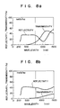
- Figs. 8a and 8b are optical characteristic diagrams of In3SbTe2.
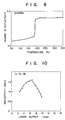
- Fig. 9 is a characteristic diagram showing changes in reflectivity by heating In3SbTe2.
- Fig. 10 is a characteristic diagram showing a relationship between the reflectivity ratio and the laser output of an optical recording medium containing an In-Te-Sb film.
- Figs. 11a and 11b are characteristics diagrams showing test results of repetitions of recording and erasing of an optical recording medium containing an In-Te-Sb film.
- Fig. 12 is a characteristic diagram of an optical recording medium having an In-Te-Sb film.
- Fig. 13 is a characteristic diagram showing differences in recording characteristics due to differences in materials of recording layer.
- Fig. 14 is a characteristic diagram showing a relationship between the number of repetitions of recording and erasing and the contrast.
- Fig. 15 is a characteristic diagram showing a relationship between the number of repetitions of recording and erasing and the average crystal grain size of the recording layer.
- Fig. 16 is an optical characteristic diagram of Bi40Se20Te40.
- Fig. 17 is a characteristic diagram showing changes in reflectivity by heating Bi40Se20Te40.
- Fig. 18 is a characteristic diagram showing a relationship between the wavelength and the light transmissivity of optical recording media having a crystalline state of a single phase of a four-component compound.
- Fig. 19 is a characteristic diagram showing a relationship between the wavelength and the spectroreflectivity of optical recording media having a crystalline state of a single phase of a four-component compound.
- Fig. 20 is a characteristic diagram showing a relationship between the reflectivity ratio and the pulse width of optical recording media having a recording layer of CuZn2InTe4 and CuInTe2, respectively.
- Fig. 21 is a characteristic diagram showing a relationship between the erasing pulse width and the crystallization temperature.
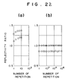
- Figs. 22(a) and 22(b) are characteristic diagrams showing a relationship between the number of repetitions of recording and erasing and the reflectivity of an optical recording medium containing CuZn2InTe4.
- the present optical recording medium is in a structure which comprises a substrate and a recording layer formed thereon.
- the substrate for use in the present invention includes a glass substrate, a metal substrate such as an aluminum substrate, an organic resin substrate such as those of polycarbonate, polymethylmethacrylate, etc.
- Fig. 1 shows one embodiment of the present optical recording medium, where a recording layer 1 is provided on a substrate 2 .
- the recording layer 1 has a thickness of preferably 50 to 200 nm and an influence of heat conduction can be disregarded in this range at the phase change.
- An electromagnetic energy can be applied to the medium from either substrate side or recording layer side.
- Fig. 2 shows that a surface protective layer 3 is further provided on the recording layer 1 .
- ceramics with a good corrosion resistance or a good wear resistance are desirably used.
- the thickness of the surface protective layer 3 is desirably 100 to 500 nm, particularly 100 to 200 nm.
- Suitable ceramics for the surface protective layer include inorganic oxides such as SiO2, Al2O3, Ta2O5, ZrO2, etc., nitrides such as Si3N4, TaN, ZrN, AlN, TiN, etc., and fluorides such as SiF, etc.
- Fig. 3 shows that a heat shielding layer 4 is provided between the substrate 2 and the recording layer 1 .
- the heat shielding layer 4 is effective when the substrate material is an organic resin.
- the same material as that for the surface protective layer can be used.
- the thickness in a range of 100 to 200 nm is quite effective for the heat shielding.
- Fig. 4 shows such a structure that the recording layer 1 is sandwiched between the substrate 2 and a glass plate 5 .
- the surface precision of the recording layer 1 can be improved to give a flat surface with much less unevenness thereby.
- Fig. 5 shows that a recess is provided on the surface of the substrate 2 and the recording layer 1 is provided over the recess.
- the space 6 formed between the substrate 2 and the recording layer 1 is filled with air. Since the air is of very poor heat conductivity, transmission of the heat through the substrate 2 can be made smaller by the air when an electromagnetic energy spot is focused onto the recording layer. That is, the desired part of the recording layer can be locally heated thereby to undergo a phase change and much accelerate the recording speed and the erasing speed.
- the electromagnetic energy must be applied to the recording layer 1 from the overhead of the glass plate 5 .
- Fig. 6 shows that a pair of substrates 2 each provided with a recording layer 1 on one side are brought into contact through a heat shielding layer 4 to make the recording layers 1 face each other, where the substrates 2 are preferably transparent glass substrates to make possible recording from both sides.
- information can be recorded by locally focusing an electromagnetic energy to the desired part of the recording layer to make the electromagnetic energy-focused part undergo a phase change.
- Recording can be made by using any of the amorphous state and the crystalline state. That is, recording is made by using one of the amorphous state and the crystalline state and erasing is made by using the other state.
- high speed recording and high speed erasing can be made by using the amorphous state for recording and by using the crystalline state for erasing. That is, desirably recording is made by focusing an electromagnetic energy spot onto the recording layer in the crystalline state, thereby phase changing the crystalline state into the amorphous state, whereas erasing is made by phase changing the amorphous state into the crystalline state, thereby returning the recorded state to the original unrecorded state.
- Reproduction can be made by detecting the state of the parts recorded by the phase change. Actually, reproduction can be carried out as optical changes.
- the optical properties of the recording layer of the present optical recording medium are locally changed by a phase change. For example, reflectivity, transmissivity, absorbance, emissivity, magnetic Kerr effect, etc. are changed by a phase change. Thus, information can be reproduced by detecting any one of these optical properties.
- the electromagnetic energy includes a laser beam, a xenon lamp, etc.
- the present optical recording medium can be used as an optical disk by providing a recording layer on a disk with tracking grooves, and also as an optical card or as a digital tape for audio appliances.
- the optical card can be provided by forming a recording layer on the tracking grooves-provided surface of a substrate.
- Fig. 7 shows a preferable structure of the optical card, where a heat shielding layer 4 is formed on a substrate 2 and a recording layer 1 is formed on the heat shielding layer 4 .
- the surface of the recording layer 1 is protected by a surface protective layer 3 .
- the audiodigital tape can be provided by forming a recording layer on the tracking grooves-provided surface of a flexible organic resin tape.
- the surface of the recording surface is desirably further protected with a protective layer.
- optical recording medium than the high speed recording and high speed erasing are a high resistance to moisture and oxidation, a high productivity, a high S/N ratio, etc. Furthermore, it is required that after repetitions of the phase change between the amorphous state and the crystalline state the same amorphous state and crystalline state can be always obtained and that these states will not change even after the optical recording medium is left in these states for a long time. The last requirement is very important for the rewritable optical recording medium.
- the conventional optical recording medium of phase exchange type between the amorphous state and the crystalline state or between one crystalline state and another crystalline state is not satisfactory in the erasing speed.
- a chalcogenide based material actually has a recording speed of actual level such as 0.2 ⁇ s, whereas its erasing speed is very low, for example, 5 ⁇ s.
- Te-based recording material has such a problem that it is readily oxidized with the moisture in the air.
- the present optical recording medium has not only high recording speed and erasing speed, but also other properties of high level.
- f 2.
- the degrees of freedom f is the numbers of variable thermodynamic quantity.
- a single phase of three-component compound has two degrees of freedom besides the temperature.
- a single phase of three-component compound has one more degree of freedom for the composition than a single phase of two-component compound. This means that the three-component compound has less occurrence of phase separation (multi-phase formatoin) against changes in the single phase composition, as compared with the two-component compound.
- the desired composition has been so far prepared by high level composition control, whereas in a single phase composition of three-component compound the single phase composition can be more readily prepared.
- This is effective for considerably increasing the productivity of optical recording medium, and also effective for local changes in the composition which occur at the repetitions of recording and erasing.
- the single phase can be maintained and the recording and erasing characteristics can be stabilized, resulting in an increase in the reliability.
- repetitions of recording and erasing can be carried out stably, resulting in an increase in the number of the repetitions.
- the crystallization from an amorphous state often involves complicated processes, e.g. nucleation, phase separation, structural relaxation, etc.
- the structural change due to the phase separation requires a long distance diffusion of atoms and thus the structure having a longer diffusion distance and a low diffusion rate (diffusion constant) has a lower crystalline rate.
- Nucleation of a plurality of phases (multi-phase) having considerably different crystal structures due to the phase separation requires a very long time owing to boundary strains.
- the long distance diffusion can be avoided by making a single crystallization phase and the crystallization can be highly accelerated by shorter distance diffusion in the order of band length.
- the strains become smaller and the nucleation can be also facilitated. Owing to the foregoing physical factors, the erasing speed of the optical recording medium comprising a recording layer of single phase is higher than that of the conventional recording medium based on the phase separation.
- the phase change between the amorphous state and the crystalline state in a single phase has a less volume change than the phase separation in a multi-phase.
- the crystalline state involve an excess volume owing to the misfit states between one phase and another phase, whereas in a single phase there is no misfit state.
- the material has a less fatigue due to the volume change that occurs at repetitions of recording and erasing, and the single phase has an improved repetition characteristic than the plurality of phases.
- the crystalline state (erasing) in the single phase has a less strain energy at the crystal grain boundary, as described before, but those in the multi-phase have a very large strain energy.
- the strain energy at the grain boundary can be measured as a grain boundary energy.
- the crystal grain growth rate will be higher with increasing grain boundary energy ⁇ . That is, the crystal grain growth is larger when the grain boundaries are composed of a multi-phase and is smaller when composed of a single phase. This means that the single crystal phase has less crystal grain growth and consequent less reduction in the S/N ratio due to the heat cycles of recording and erasing.
- the conventional recording layer materials are in a mixture of phases containing additive elements without any consideration of stoichiometry of a compound only to improve their characteristics, and thus the chemical bond correlations among the atoms therselves are indefinite in such a mixture of phases.
- the present invention provides an optical recording medium having a recording layer composed of a chemically stoichiometric compound, based on the finding that such a mixture of phases (multi-phase) does not improve the overall characteristics of an optical recording medium.
- a chalcogenide-based compound is a covalent bond solid.
- the covalent bond solid herein referred to is a solid, where the bonds of atoms themselves are mostly of the covalent bond type, and quantitively a solid whose covalent bond degree ⁇ c , for example, by LCAO method (or local atomic orbital method) is 0.5 or more (W.A. Harrison: Electronic Structure and Physical Properties of Solids, translated by Tadanobu Kojima, Kazuko Kojima and Eizaburo Yamada and published by Gendai Kogaku-sha, Japan, page 117).
- the resistance to moisture and oxidation of a recording layer can be considerably improved by making the recording layer from a covalent bond solid of three-component compound.
- the solid of three-component compound is a chemically stoichiometric composition or is very approximate thereto, and thus is saturated with the covalent bonds and the excess valence electron density is so small that no bonds are formed between the oxygen atoms or between the water molecules from the outside, that is, the slid undergoes neither oxidation nor hydration (hydroxidation).
- the stoichiometric compound is generally thermodynamically highly stable and thus undergoes no oxidation or hydration-decomposition with the result of less liberation of toxic single elements.
- an optical recording medium whose recording layer is composed of a suitable single phase of three-component compound at erasing can effectively overcome the problems of the conventional materials for the recording layer owing to the physico-chemical characteristics of the recording layer composed of a single phase of three-component compound and can further improve the characteristics of the optical recording medium. It has been found that the physico-chemical characteristics of a recording layer composed of a single phase of three-component compound do not improve the characteristics of the optical recording medium as independent factors, but act integrally to bring about a synergistic effect.
- the present invention is also applicable to a recording layer composed of a single phase of four-component compound or higher multi-component compound.
- the three-component compounds for use in the present invention are In3SbTe2, AgSbTe2, (AuSb)2Te3, Bi2SeTe2, and Sb2SnTe4.
- a four-component compound for use in the single phase in the recording layer includes, for example, (Cu,Hg)12Sb4Se13, (Ni,Pd)2SbTe, Pd(Sb,Bi)Te, CuPbBiSe3, CuCd2GaSe4, (Cu,Ga)CdSe2, CuCd2InSe4, CuAl4InSe8, CuCdSiSe4, CrCuSnSe4, CuCoGeSe4, Cu2CoSnSe4, CuZn2GaSe4, Cu2FeGeSe4, Cu2FeSiSe4, Cu2FeSnSe 3.8-4 , Cu2MnGeSe4, CuMnSiSe4, CuMnSnSe4, Cu2HgSiSe4, Cu2NiGeSe4, Cu3FeTl2Se4, Cu3Tl2FeSe4, CuZn2InSe4, Cu2ZnSiSe4,
- vapor deposition films were prepared as recording layers.
- the structure of the optical recording medium was as shown in Fig. 2, and a laser beam was focused on the optical recording medium from the overhead of the substrate.
- the substrate was quartz glass plate, a rigid glass plate or a polycarbonate (PC) resin disk, each 1.2 mm in thickness.
- As a protective layer an inorganic layer of SiO2, AlN, Ta2O5, TiN, Cr2O3, SiN, SiC, GeN, ZrO2, TiO2, ZnS, or SiC was formed on the recording layer by RF sputtering.
- the thickness of the protective layer was 100 to 500 nm, depending upon the interference conditions of the beam transmitted through the recording layer.
- the desired (target) compositions of the recording films composed of a single phase of three-component compounds thus prepared are shown below: Bi2SeTe2, Ga4GeSe8, Sb2SeTe4, GaGeSe3, Au2SeTe, AgGaSe2, (AuSb)2Te3, Ag9GaSe6.
- Vapor deposition procedure applicable for forming the single phase of three-component compound includes a single source vapor deposition procedure, a two-source vapor deposition procedure and a three-source vapor deposition procedure as conventional procedures, as shown in the following Table 1.
- an alloy of the desired composition is prepared in advance, and is subjected to the vapor deposition.
- a two-component alloy is prepared in advance and is subjected to vapor deposition as one vapor source together with a simple element as another vapor source to form a single phase of three-component compound.
- the three simple elements are subjected to vapor deposition at the same time to form a single phase of three-component compound.
- the present vapor deposition procedure is a two-source procedure as in the conventional procedure, but a remarkable difference from the conventional two-source vapor deposition procedure using a combination of a two-component alloy as one vapor source and a single element as another source is that a combination of a pair of two-component compounds is used in the present invention.
- Recording layers each composed of a single phase of the desired three-component compound as listed above were prepared according to the individual vapor deposition procedures and analyzed. The results of analysis are also shown in Table 1, where the cross mark (x) shows a considerable deviation from the desired compound composition and the circle mark (o) shows a substantially desired compound composition.
- Table 2 shows analytical results of films prepared as a recording layer from a single phase, three-component compound, CuInTe2, according to the conventional vapor deposition procedures and the present vapor deposition procedure.
- Cu25In25Te50 (in % by atom) as a vapor source matirial for the conventional single source vapor deposition procedure was melted and alloyed in a Siliconit furnace and used as the vapor source.
- the individual vapor sources were placed on tungsten or molybdenum boats in a vapor deposition chamber, respectively, and the vapor deposition chamber was evacuated to a vacuum degree of 5 x 10 ⁇ 6 Torr and then the vapor sources were subjected to vapor deposition each to form a vapor deposition film on a substrate to a film thickness of 80 to 120 nm.
- the thus obtained films were subjected to ICP analysis.
- no desired compositions were obtained in the conventional procedures, whereas the film obtained by simultaneous vapor deposition of the two-component compounds, InTe and CuTe, according to the present invention had a substantially desired composition.
- a two-source resistance-heating vapor deposition chamber was used as a vapor deposition chamber for the present invention.
- Table 3 shows analytical results of films composed of a single phase of three-component compound, In3SbTe2, prepared according to the conventional vapor deposition procedures and the present vapor deposition procedure under the same preparation conditions as in Procedure 2. As is apparent from the analytical results of Table 3, the present vapor deposition procedure was distinguished in obtaining a film of desired composition, as in Procedure 2.
- Figs. 8a and 8b Optical characteristics of In3SbTe2 are shown in Figs. 8a and 8b.
- Fig. 8a shows spectroscopic characteristics of an optical recording medium having a film prepared in the same manner as above as a recording layer and a protective film of SiO2 having a thickness of 100 nm, formed on the recording layer.
- Fig. 8b shows spectroscopic characteristics of the same optical recording medium as above, heated up to 350°C, that temperature for 5 minutes and then slowly cooled.
- the semiconductor laser wavelength of 830 nm the reflectivity was increased to 40% from 34% and the transmissivity was decreased to 1% from 8% by the heat treatment. This shows that the optical characteristics were greatly changed by a phase change from the amorphous state to the crystalline state.
- Fig. 9 shows measurement results of dynamic change in the reflectivity by heating, where the reflectivity abruptly increased at 188°C. This shows that the present optical recording medium can undergo high speed erasing.
- the film prepared according to the present vapor deposition procedure had a analytical composition of In51Sb17Te32 (in % by atom) and it seems that a single phase of three-component compound, In3SbTe2, was formed. According to the phase diagram of pseudo-binary system of InTe-InSb, the melting point at a metastable state of In3SbTe2 is 568°C and the single phase dominates just up to the melting point.
- an amorphous state can be obtained by heating to higher than the single melting point, followed by quenching. Since the melting point of a single phase compound is substantially single, the single phase compound will melt at a definite temperature at that time, and thus the high speed recording can be made. Furthermore, since the single phase of three-component compound can dominate against heating just up to the melting point, a phase change from the amorphous state to the crystalline state can be made at the erasing by heating just up to the melting point from the crystallization temperature without phase separation. Since the crystallization is 188°C, as seen from Fig. 9, superheating by 380°C can be obtained. The absence of phase separation unnecessitates a long distance diffusion and thus high speed erasing can be made.
- An In-Te-Sb film was formed on a transparent glass substrate or a polycarbonate substrate to a film thickness of 100 mm by DC magnetron sputtering.
- the sputtering target was prepared by melting in an Ar atmosphere.
- the sputtering conditions were an output power of 100 W, an initial vacuum degree of 8.5 x 10 ⁇ 5 Pa, an Ar partial pressure of 20 m Torr with water cooling of the substrate.
- the thus formed In-Te-Sb film was found by analysis to have a composition of In49Sb20Te31 (in % by atom), which was substantially identical with the composition of the compound obtained by vapor deposition.
- the spectroscopic characteristics and crystallization temperature were substantially identical with those of the vapor deposited film, and the same reproducibility as that of the vapor deposited film was obtained.
- Fig. 10 shows recording and erasing characteristics of an optical recording medium having the sputtering film prepared in the same manner as above as a recording layer and a SiO2 film having a thickness of 100 nm, formed in the same manner as in Example 1, where the initial state is an amorphous state and the reflectivity ratio increases by increasing the laser output power from 2 mW to 4 mW and further to 6 mW.
- This increase in the reflectivity ratio means a contribution to a phase change from the amorphous state to the crystalline state.
- the laser output power With further increase of the laser output power to 7 mW or higher, the recording is initiated, and the reflectivity ratio starts to decrease.
- Figs. 11a and 11b show results of repetitions of recording and erasing of the present recording medium, that is, the results obtained by repeating recording and erasing 10 times as the initialization, thereby stabilizing the optical recording medium and then by making 106 repetitions of recording and erasing under the recording conditions of laser output power of 13 mW and pulse width of 0.02 ⁇ m and the erasing conditions of 8 mW and and 0.03 ⁇ s, where the average contrast was 18% at the repetition test.
- the present optical recording medium can overwrite for 0.03 ⁇ s, that is, can erase the recorded information for 0.03 ⁇ s and record new information at the same speed.
- the contrast is still as small as 18% in this test, but can be increased to about 25% by optimizing the film thicknesses of the recording layer and the protective layer and the materials of the protective layer.
- Fig. 12 shows a characteristic map of the present optical recording medium.
- the present optical recording medium can undergo high speed recording and erasing because a recording layer composed of a single phase of three-component compound is subjected to recording just above the melting point and to erasing just below the melting point.
- the present optical recording medium has a broad erasing region as a characteristic.
- the film breakage hardly occurs even at a high laser output power and much higher speed recording and erasing can be made with a laser of higher output power.
- Fig. 13 shows static state recording test results of optical recording media having a recording layer of In-Te-Sb system, that is, In50Sb15Te35, a composition that precipitates In3SbTe2 in a single phase at the crystallization; In17Sb48Te35, a composition that precipitate compounds in two phases; In20Sb15Te65, a composition that precipitates Te in a single phase.
- the recording conditions were that the pulse width was gradually made longer at the laser output power of 12 mW.
- the initial states were just the same states as the films were formed and were each identified to be amorphous states.
- the reflectivity increased at first by crystallization and melting started by making the pulse width larger, thereby effecting partial heating to a temperature over the melting point. That is, the recording layer was brought into a recording state, whereby the reflectivity was decreased. It was found by comparing the results of the three compositions that the composition that precipitates the In3SbTe in a single phase had the highest erasing and recording speeds, the composition that precipitate the compounds in two phases had the next highest speeds and the composition that precipitates Te in a single phase had the lowest speeds. That is, the single phase region of three-component compound had the best recording and erasing characteristics.
- Table 4 shows the results of durability tests of the compositions given in the Table 4 at a temperature of 40°C and a humidity of 90% for 10 days.
- Test pieces were optical recording media each having a recording layer composed of one of the compositions and formed to a thickness of 100 nm on a glass substrate and a protective film of SiO2 formed to a thickness of 100 nm on the recording layer and having been subjected to pulse recording with 12 mW and 0.5 ⁇ s.
- the single phase composition of In3SbTe2 and a double phase composition of In3SbTe2 + In2Te3 had no change, whereas the composition that precipitates In2Te3 + Te had a change in the recording layer and had a higher transmissivity and it was found by microscopic observation that its recorded signal was obscure, because it seems that Te was changed to TeO x .
- Te exists as a stable compound, it is saturated with divalent bonds and never undergoes oxidation even in an oxidizing atmosphere, whereas when Te is precipitated as a simple substance, it undergoes a phase change from the amorphous state to the crystalline state even at room temperature or it is oxidized to TeO x .
- the recording layer is deficient in stability. In other words, it is very important to use a recording layer having a composition range that never precipitates an elemental simple substance at the crystallization.
- Figs. 14 and 15 show relationships between the contrast and the average crystal grain size when recording and erasing are repeated, where repetition characteristics of single phase, three-component composition of a three-component compound In3SbTe2 and two-phase, three-component composition of two-component compounds Sb2Te3 + In2Te3 are given.
- the single phase, three-component composition had no change in the contrast after 106 repetitions of recording and erasing, whereas the contrast of the two-phase, three-component composition of Sb2Te3 + In2Te3 was about 20% lowered after 106 repetitions.
- Fig. 15 shows the average crystal grain sizes after 102 repetitions, 104 repetitions and 106 repetitions.
- the single phase, three-component composition of a three-component compound had substantially equal crystal grain sizes throughout all the repetitions, whereas the crystal grain sizes of the two-phase, three-component composition that precipitates two-component compounds in two phases had a tendency to become larger with increasing number of repetitions. This is because, when two two-component compounds having different surface energies are formed in two phases, the surface energies will be higher than at the crystal grain boundaries of the same species compounds themselves and thus a change takes place in such a direction as to reduce the surface area. That is, the repetition characteristics of the two-phase, three-component composition that precipitates two-component compounds in two phases are not better than those of the single phase composition of three-component compound.
- the Bi-Se-Te system has a three-component compound of Bi40Se20Te40.
- a film of the composition was formed as a recording layer on a substrate by vapor deposition.
- vapor sources Bi2Te3 and SiSe were prepared by melting and subjected to two-source vapor deposition at an initial vacuum degree of 3 x 10 ⁇ 6 Torr with water cooling of the substrate to form the film. Then, a protective film of SiO2 was formed on the recording layer to a thickness of 100 nm to obtain an optical recording medium.
- Fig. 16 shows optical characteristics of the film of Bi40Se20Te40 just as vapor deposited, where the reflectivity is 27.0%, the transmissivity 2.3% and the absorbance 70.7 at a wavelength of 830 nm.
- Fig. 17 shows changes in the reflectivity when the optical recording medium was heated at a temperature increase rate of 20°C/min, where the reflectivity takes a sharp rise at 118°C, which contributes to a phase change from the amorphous state to the crystalline state. It can be seen therefrom that the crystallization takes place within a very narrow temperature range and thus the single phase composition of the three-component compound can perform high speed erasing.
- Table 5 shows analytical results of films of single phase, three-component compound, AgSbTe2, prepared according to the conventional vapor deposition procedures and the present vapor deposition procedure in the same manner as in Procedure 2 above.
- the desired composition was not obtained according to the conventional procedures whereas the substantially satisfactory composition as desired was obtained according to the present invention.
- a film of CuZn2InT4 as an example of single phase, four-component compound was formed on a substrate in a DC magnetron sputtering chamber.
- the sputtering target was prepared by melting in an Ar atmosphere at an output power of 100 W, an initial vacuum degree of 8.5 x 10 ⁇ 5 Torr and an Ar partial pressure of 20 m Torr with water cooling of the substrate.
- This alloy film can be likewise formed also by vacuum vapor deposition.
- Fig. 18 shows an example of adding Zn for improving the light absorption to CuInTe2 to make CuZn2InTe4, whereby the transmissivity at a semiconductor laser wavelength of 830 nm was reduced to 9% from 18% at equal thicknesses of 100 nm, and thus the absorbance was increased.
- the power of semiconductor laser on the film surface on the substrate that can be output up to now is about 15 mW and thus the recording speed can be increased by efficient absorption of the laser beam with such power.
- Fig. 19 shows changes in the reflectivity when an optical recording medium having a recording layer of CuInTe2 and that having a recording layer of CuZn2InTe4 were heated.
- the crystallization temperature due to changes in the reflectivity was increased from 200°C to 420°C, though the reflectivity at room temperature was substantially the same therebetween.
- Such a high crystallization temperature shows that the stability of amorphous state is high at room temperature.
- Fig. 20 shows a reflectivity ratio when an optical recording medium having a recording layer of CuInTe2 and that having a recording layer of CuZn2InTe4 were exposed to a laser pulse of 10 mW.
- a laser pulse 10 mW.
- CuZn2InTe4 had a higher crystallization temperature than that of CuInTe2, and thus was not crystallized unless irradiated with a relatively strong laser of 12 mW, but its crystallization speed was much accelerated. That is, high speed erasing was possible.
- the present recording layer materials have a high crystallization temperature and high speed erasing can be made with a relatively strong laser beam.
- Fig. 21 shows erasing pulse width obtained for recording layers having different crystallization temperatures from the results of Fig. 20, where a single phase, four-component compound having the highest crystallization temperature has the shortest erasing pulse width and thus can undergo the fastest erasing.
- the foregoing characteristics can be obtained with compound composition comprising 10 to 15% of Cu, 20 to 30% of Zn and 8 to 17% of In, the balance being Te and containing a single phase, four-component compound as the main component.
- Figs. 22a and 22b show repetition characteristics of an optical recording medium having a recording layer of CuZn2InTe4, where distinguished repetition characteristics can be obtained owing to the single phase, 4-component compound without any fear of phase separation.
Landscapes
- Chemical & Material Sciences (AREA)
- Inorganic Chemistry (AREA)
- Thermal Transfer Or Thermal Recording In General (AREA)
- Optical Record Carriers And Manufacture Thereof (AREA)
Description
- This invention relates to a rewritable optical recording medium that can optically record, reproduce and erase information by electromagnetic energy such as light and heat, and to methods for recording and reproducing information on the optical recording medium and for recording, reproducing and erasing recorded information on the optical recording medium. Furthermore, the present invention relates to an article utilizing the properties of the optical recording medium.
- Recently, research and development have been vigorously made on information recording media capable of recording information at desired parts at a high density and a high speed, and optical recording media capable of recording and reproducing information by irradiation of laser beam spot and erasing the recorded information and rewriting new information by the laser beam have been proposed.
- The conventional optical recording media can be classified into various types such as a pit-forming type, a bubble or uneven surface-forming type, a photomagnetic type, a phase change type, etc. on the basis of what physical change is brought to the medium when heated by a laser beam spot, 1.5 µm in diameter, as disclosed in Nikkei Electronics January 4 issue (1982), page 86 et seq. under the title "Optical disk memory that has been just used in image files".
- Among these types, only optical recording media of phase change type are rewritable. So far proposed optical recording media of phase change type are those having a thin film comprising a composition containing a chalcogenide based material or a lower oxide (Japanese Patent Publication No. 47-26897).
- The optical recording media of phase change type include those based on a phase change between the amorphous state and the crystalline state or between one crystalline state and another crystalline state. Chalcognide-based substances mainly belong to the phase change type between the amorphous state and the crystalline state and include those disclosed in the Japanese Patent Publication No. 47-26897 and tellurium compounds, etc. disclosed in Japanese Patent Application Kokai (Laid-open) No. 60-253034. Cu-Al-Ni alloy or In-Sb alloy disclosed in Japanese Patent Application Kokai (Laid-open) No. 60-46339 belong to the phase change type between the crystalline states. In these optical recording media, recording and erasing are carried out by reversibly changing the structural state from one to another or vice versa. In those media of phase change type between the amorphous state and the crystalline state, recording and erasing are carried out by using the amorphous state for a recording state and the crystalline state for an unrecording state.
- One of the important requirements for an optical recording medium is higher speed recording and erasing.
- Conventional, rewritable optical recording media of phase change type, including those of phase change type between the amorphous state and the crystalline state and those of phase change type between one crystalline state and another crystalline state have such a problem as low speed erasing.
- EP-A-212 336 and EP-A-239 166 describe some recording layers switchable between crystalline and amorphous states, made of three-component compounds, including some In Sb Te compounds.
- An object of the present invention is to provide a rewritable optical recording medium of phase change type between an amorphous and a crystalline state, which is capable of recording and erasing information at a high speed.
- According to the present invention, there is provided a recording medium as set out in
claim 1. - Within the present invention for example high speed recording and erasing has been actually attained by an optical recording medium comprising a recording layer whose crystalline state is composed of a single phase of a four-component compound.
- The four-component compound herein referred to means a compound having a crystal structure directly determined from the Bragg's diffraction angle in the X-ray diffraction.
- In the present optical recording medium, the crystalline state of the recording medium may not always be composed only of a single phase entirely of one of the kinds (i), (ii) and (iii) of
claim 1. - That is, the crystalline state may be composed of a single phase mainly of one of the kinds (i), (ii) and (iii) of
claim 1. - The recording layer can be formed from a raw-material composed of a mixture of components that can form the desired material by any thin film-forming means such as sputtering, vapor deposition, coating, plating, etc. When the mixture of components as the raw material is deviated from a composition capable of forming the desired material, a single phase containing the deviated component or components is formed, but is, of course, practically applicable. Usually, the single phase must contain at least 90% by atom of the material specified at (i), (ii) and (iii) of
claim 1. That is, the amount of such material must not be less than 90% by atom in the single phase. - The recording layer can contain other components than those which form the material specified at (i), (ii) and (iii) of
claim 1, within such a range that the crystal structure of the single phase of the material can be maintained. The crystallization temperature and the melting temperature of the compound can be controlled and the sensitivity of recording and erasing can be increased thereby. Thus, in the case of the single phase of a three-component compound In₃SbTe₂, the melting point of the three component compound can be lowered and the sensitivity of recording and erasing can be further increased by adding at least one of silver (Ag), tin (Sn) and copper (Cu) thereto. In the case of In₃SbTe₂, the total content of silver, tin and copper is not more than 5% by atom. So long as the total content of silver, tin and copper is not more than 5% by atom, these additive components can undergo solid solution in the crystals, maintaining the crystalline state of the single phase of the three-component compound. However, when the content of silver, tin and copper increases and exceeds 10% by atom in total, another compound will be formed, resulting in phase separation and losing the single phase. - The present invention will be described in detail below, referring to the drawings.
- Figs. 1 to 6 are schematic cross-sectional views showing the structures of the present optical recording media.
- Fig. 7 is a schematic cross-sectional view in part of an optical card according to one embodiment of the present invention.
- Figs. 8a and 8b are optical characteristic diagrams of In₃SbTe₂.
- Fig. 9 is a characteristic diagram showing changes in reflectivity by heating In₃SbTe₂.
- Fig. 10 is a characteristic diagram showing a relationship between the reflectivity ratio and the laser output of an optical recording medium containing an In-Te-Sb film.
- Figs. 11a and 11b are characteristics diagrams showing test results of repetitions of recording and erasing of an optical recording medium containing an In-Te-Sb film.
- Fig. 12 is a characteristic diagram of an optical recording medium having an In-Te-Sb film.
- Fig. 13 is a characteristic diagram showing differences in recording characteristics due to differences in materials of recording layer.
- Fig. 14 is a characteristic diagram showing a relationship between the number of repetitions of recording and erasing and the contrast.
- Fig. 15 is a characteristic diagram showing a relationship between the number of repetitions of recording and erasing and the average crystal grain size of the recording layer.
- Fig. 16 is an optical characteristic diagram of Bi₄₀Se₂₀Te₄₀.
- Fig. 17 is a characteristic diagram showing changes in reflectivity by heating Bi₄₀Se₂₀Te₄₀.
- Fig. 18 is a characteristic diagram showing a relationship between the wavelength and the light transmissivity of optical recording media having a crystalline state of a single phase of a four-component compound.
- Fig. 19 is a characteristic diagram showing a relationship between the wavelength and the spectroreflectivity of optical recording media having a crystalline state of a single phase of a four-component compound.
- Fig. 20 is a characteristic diagram showing a relationship between the reflectivity ratio and the pulse width of optical recording media having a recording layer of CuZn₂InTe₄ and CuInTe₂, respectively.
- Fig. 21 is a characteristic diagram showing a relationship between the erasing pulse width and the crystallization temperature.
- Figs. 22(a) and 22(b) are characteristic diagrams showing a relationship between the number of repetitions of recording and erasing and the reflectivity of an optical recording medium containing CuZn₂InTe₄.
- The present optical recording medium is in a structure which comprises a substrate and a recording layer formed thereon. The substrate for use in the present invention includes a glass substrate, a metal substrate such as an aluminum substrate, an organic resin substrate such as those of polycarbonate, polymethylmethacrylate, etc.
- Fig. 1 shows one embodiment of the present optical recording medium, where a
recording layer 1 is provided on asubstrate 2. Therecording layer 1 has a thickness of preferably 50 to 200 nm and an influence of heat conduction can be disregarded in this range at the phase change. An electromagnetic energy can be applied to the medium from either substrate side or recording layer side. - Fig. 2 shows that a surface
protective layer 3 is further provided on therecording layer 1. For the surfaceprotective layer 3, ceramics with a good corrosion resistance or a good wear resistance are desirably used. The thickness of the surfaceprotective layer 3 is desirably 100 to 500 nm, particularly 100 to 200 nm. Suitable ceramics for the surface protective layer include inorganic oxides such as SiO₂, Al₂O₃, Ta₂O₅, ZrO₂, etc., nitrides such as Si₃N₄, TaN, ZrN, AlN, TiN, etc., and fluorides such as SiF, etc. - Fig. 3 shows that a
heat shielding layer 4 is provided between thesubstrate 2 and therecording layer 1. Theheat shielding layer 4 is effective when the substrate material is an organic resin. As the material for theheat shielding layer 4, the same material as that for the surface protective layer can be used. The thickness in a range of 100 to 200 nm is quite effective for the heat shielding. - Fig. 4 shows such a structure that the
recording layer 1 is sandwiched between thesubstrate 2 and aglass plate 5. The surface precision of therecording layer 1 can be improved to give a flat surface with much less unevenness thereby. - Fig. 5 shows that a recess is provided on the surface of the
substrate 2 and therecording layer 1 is provided over the recess. Thespace 6 formed between thesubstrate 2 and therecording layer 1 is filled with air. Since the air is of very poor heat conductivity, transmission of the heat through thesubstrate 2 can be made smaller by the air when an electromagnetic energy spot is focused onto the recording layer. That is, the desired part of the recording layer can be locally heated thereby to undergo a phase change and much accelerate the recording speed and the erasing speed. In the structure as shown in Fig. 5, the electromagnetic energy must be applied to therecording layer 1 from the overhead of theglass plate 5. - Fig. 6 shows that a pair of
substrates 2 each provided with arecording layer 1 on one side are brought into contact through aheat shielding layer 4 to make the recording layers 1 face each other, where thesubstrates 2 are preferably transparent glass substrates to make possible recording from both sides. - In the present invention, information can be recorded by locally focusing an electromagnetic energy to the desired part of the recording layer to make the electromagnetic energy-focused part undergo a phase change. Recording can be made by using any of the amorphous state and the crystalline state. That is, recording is made by using one of the amorphous state and the crystalline state and erasing is made by using the other state.
- According to a specific embodiment of the present invention, high speed recording and high speed erasing can be made by using the amorphous state for recording and by using the crystalline state for erasing. That is, desirably recording is made by focusing an electromagnetic energy spot onto the recording layer in the crystalline state, thereby phase changing the crystalline state into the amorphous state, whereas erasing is made by phase changing the amorphous state into the crystalline state, thereby returning the recorded state to the original unrecorded state.
- Reproduction can be made by detecting the state of the parts recorded by the phase change. Actually, reproduction can be carried out as optical changes.
- The optical properties of the recording layer of the present optical recording medium are locally changed by a phase change. For example, reflectivity, transmissivity, absorbance, emissivity, magnetic Kerr effect, etc. are changed by a phase change. Thus, information can be reproduced by detecting any one of these optical properties.
- As the electromagnetic energy, photo energy, electron energy, etc. can be utilized. The photo energy includes a laser beam, a xenon lamp, etc.
- The present optical recording medium can be used as an optical disk by providing a recording layer on a disk with tracking grooves, and also as an optical card or as a digital tape for audio appliances.
- The optical card can be provided by forming a recording layer on the tracking grooves-provided surface of a substrate. Fig. 7 shows a preferable structure of the optical card, where a
heat shielding layer 4 is formed on asubstrate 2 and arecording layer 1 is formed on theheat shielding layer 4. The surface of therecording layer 1 is protected by a surfaceprotective layer 3. - The audiodigital tape can be provided by forming a recording layer on the tracking grooves-provided surface of a flexible organic resin tape. The surface of the recording surface is desirably further protected with a protective layer.
- Other requirements for an optical recording medium than the high speed recording and high speed erasing are a high resistance to moisture and oxidation, a high productivity, a high S/N ratio, etc. Furthermore, it is required that after repetitions of the phase change between the amorphous state and the crystalline state the same amorphous state and crystalline state can be always obtained and that these states will not change even after the optical recording medium is left in these states for a long time. The last requirement is very important for the rewritable optical recording medium.
- The conventional optical recording medium of phase exchange type between the amorphous state and the crystalline state or between one crystalline state and another crystalline state is not satisfactory in the erasing speed. For example, a chalcogenide based material actually has a recording speed of actual level such as 0.2 µs, whereas its erasing speed is very low, for example, 5 µs.
- Furthermore, the Te-based recording material has such a problem that it is readily oxidized with the moisture in the air.
- The present optical recording medium has not only high recording speed and erasing speed, but also other properties of high level.
- The function of the present invention will be described in detail below, referring to a recording layer whose cristalline state is of a single phase of three-component compound.
- Thermodynamic phase rule can be given by the following equation under a constant pressure, for example, the atmospheric pressure:

where C stands for the number of components, p the number of phases and f the degrees of freedom. - In a single phase of a three-component compound, C=3 and p=1, and thus the degrees of freedom f=3. Likewise, in a single phase of a two-component compound, f=2. The degrees of freedom f is the numbers of variable thermodynamic quantity. For example, a single phase of three-component compound has two degrees of freedom besides the temperature. In other words, a single phase of three-component compound has one more degree of freedom for the composition than a single phase of two-component compound. This means that the three-component compound has less occurrence of phase separation (multi-phase formatoin) against changes in the single phase composition, as compared with the two-component compound. Thus, in the formation of a recording layer by vapor deposition or sputtering, the desired composition has been so far prepared by high level composition control, whereas in a single phase composition of three-component compound the single phase composition can be more readily prepared. This is effective for considerably increasing the productivity of optical recording medium, and also effective for local changes in the composition which occur at the repetitions of recording and erasing. Thus, the single phase can be maintained and the recording and erasing characteristics can be stabilized, resulting in an increase in the reliability. Furthermore, repetitions of recording and erasing can be carried out stably, resulting in an increase in the number of the repetitions. The crystallization from an amorphous state often involves complicated processes, e.g. nucleation, phase separation, structural relaxation, etc. The structural change due to the phase separation requires a long distance diffusion of atoms and thus the structure having a longer diffusion distance and a low diffusion rate (diffusion constant) has a lower crystalline rate. Nucleation of a plurality of phases (multi-phase) having considerably different crystal structures due to the phase separation requires a very long time owing to boundary strains. However, the long distance diffusion can be avoided by making a single crystallization phase and the crystallization can be highly accelerated by shorter distance diffusion in the order of band length. Furthermore, since the crystallization proceeds in the same crystal structure, the strains become smaller and the nucleation can be also facilitated. Owing to the foregoing physical factors, the erasing speed of the optical recording medium comprising a recording layer of single phase is higher than that of the conventional recording medium based on the phase separation.
- The phase change between the amorphous state and the crystalline state in a single phase has a less volume change than the phase separation in a multi-phase. In the multi-phase, the crystalline state involve an excess volume owing to the misfit states between one phase and another phase, whereas in a single phase there is no misfit state. In other words, the material has a less fatigue due to the volume change that occurs at repetitions of recording and erasing, and the single phase has an improved repetition characteristic than the plurality of phases.
- The crystalline state (erasing) in the single phase has a less strain energy at the crystal grain boundary, as described before, but those in the multi-phase have a very large strain energy. The strain energy at the grain boundary can be measured as a grain boundary energy. According to the teaching of crystal grain growth rate in the metallurgy, the crystal grain growth rate dD/dt has a relationship with boundary energy γ, given by the following equation:

where D is an average diameter of crystal grains and k a constant. - Thus, the crystal grain growth rate will be higher with increasing grain boundary energy γ. That is, the crystal grain growth is larger when the grain boundaries are composed of a multi-phase and is smaller when composed of a single phase. This means that the single crystal phase has less crystal grain growth and consequent less reduction in the S/N ratio due to the heat cycles of recording and erasing.
- As described above, the conventional recording layer materials are in a mixture of phases containing additive elements without any consideration of stoichiometry of a compound only to improve their characteristics, and thus the chemical bond correlations among the atoms therselves are indefinite in such a mixture of phases. The present invention provides an optical recording medium having a recording layer composed of a chemically stoichiometric compound, based on the finding that such a mixture of phases (multi-phase) does not improve the overall characteristics of an optical recording medium. Generally, a chalcogenide-based compound is a covalent bond solid. The covalent bond solid herein referred to is a solid, where the bonds of atoms themselves are mostly of the covalent bond type, and quantitively a solid whose covalent bond degree αc, for example, by LCAO method (or local atomic orbital method) is 0.5 or more (W.A. Harrison: Electronic Structure and Physical Properties of Solids, translated by Tadanobu Kojima, Kazuko Kojima and Eizaburo Yamada and published by Gendai Kogaku-sha, Japan, page 117). The resistance to moisture and oxidation of a recording layer can be considerably improved by making the recording layer from a covalent bond solid of three-component compound. The solid of three-component compound is a chemically stoichiometric composition or is very approximate thereto, and thus is saturated with the covalent bonds and the excess valence electron density is so small that no bonds are formed between the oxygen atoms or between the water molecules from the outside, that is, the slid undergoes neither oxidation nor hydration (hydroxidation). Further, the stoichiometric compound is generally thermodynamically highly stable and thus undergoes no oxidation or hydration-decomposition with the result of less liberation of toxic single elements.
- It can be seen from the foregoing that an optical recording medium whose recording layer is composed of a suitable single phase of three-component compound at erasing can effectively overcome the problems of the conventional materials for the recording layer owing to the physico-chemical characteristics of the recording layer composed of a single phase of three-component compound and can further improve the characteristics of the optical recording medium. It has been found that the physico-chemical characteristics of a recording layer composed of a single phase of three-component compound do not improve the characteristics of the optical recording medium as independent factors, but act integrally to bring about a synergistic effect. The present invention is also applicable to a recording layer composed of a single phase of four-component compound or higher multi-component compound.
- The three-component compounds for use in the present invention are In₃SbTe₂, AgSbTe₂, (AuSb)₂Te₃, Bi₂SeTe₂, and Sb₂SnTe₄.
- A four-component compound for use in the single phase in the recording layer includes, for example, (Cu,Hg)₁₂Sb₄Se₁₃, (Ni,Pd)₂SbTe, Pd(Sb,Bi)Te, CuPbBiSe₃, CuCd₂GaSe₄, (Cu,Ga)CdSe₂, CuCd₂InSe₄, CuAl₄InSe₈, CuCdSiSe₄, CrCuSnSe₄, CuCoGeSe₄, Cu₂CoSnSe₄, CuZn₂GaSe₄, Cu₂FeGeSe₄, Cu₂FeSiSe₄, Cu₂FeSnSe3.8-4, Cu₂MnGeSe₄, CuMnSiSe₄, CuMnSnSe₄, Cu₂HgSiSe₄, Cu₂NiGeSe₄, Cu₃FeTl₂Se₄, Cu₃Tl₂FeSe₄, CuZn₂InSe₄, Cu₂ZnSiSe₄, Ga₂InAsSe₃, AgAl₄InSe₈, PbBi₂(Se,Te)₄, AlNa₃SiTe₄, CuCd₂GaTe₄, CuGd₂InTe₄, AgCd₂InTe₄, CuZn₂GaTe₄, Cu₃FeTl₂Te₄, CuZn₂InTe₄, PdBi₂(Se,Te)₄ and AgInAl₄Te₈.
- Some procedures for forming compounds used in the present invention, and other analogous compounds, will now be described.
- In order to find the function of an optical recording medium, vapor deposition films were prepared as recording layers. The structure of the optical recording medium was as shown in Fig. 2, and a laser beam was focused on the optical recording medium from the overhead of the substrate. The substrate was quartz glass plate, a rigid glass plate or a polycarbonate (PC) resin disk, each 1.2 mm in thickness. As a protective layer, an inorganic layer of SiO₂, AlN, Ta₂O₅, TiN, Cr₂O₃, SiN, SiC, GeN, ZrO₂, TiO₂, ZnS, or SiC was formed on the recording layer by RF sputtering. The thickness of the protective layer was 100 to 500 nm, depending upon the interference conditions of the beam transmitted through the recording layer. The desired (target) compositions of the recording films composed of a single phase of three-component compounds thus prepared, which include compounds used in the present invention, are shown below: Bi₂SeTe₂, Ga₄GeSe₈, Sb₂SeTe₄, GaGeSe₃, Au₂SeTe, AgGaSe₂, (AuSb)₂Te₃, Ag₉GaSe₆. Ge₂SeTe, In₃SbTe₂, Bi₄GeTe₇, AgInTe₂, AgTn₅Te₃, Ag₈GeTe₆, CuIn₅Te₈, CuInTe₂, Cu₂GeTe₃, Cu₂SnTe₃, Cu₃SbSe₄ and AgInSe .
- Vapor deposition procedure applicable for forming the single phase of three-component compound includes a single source vapor deposition procedure, a two-source vapor deposition procedure and a three-source vapor deposition procedure as conventional procedures, as shown in the following Table 1.

- According to the conventional simple source vapor evaporation procedure, an alloy of the desired composition is prepared in advance, and is subjected to the vapor deposition. According to the conventional two-source vapor deposition procedure, a two-component alloy is prepared in advance and is subjected to vapor deposition as one vapor source together with a simple element as another vapor source to form a single phase of three-component compound. According to the conventional three-source vapor deposition procedure, the three simple elements are subjected to vapor deposition at the same time to form a single phase of three-component compound. On the other hand, the present vapor deposition procedure is a two-source procedure as in the conventional procedure, but a remarkable difference from the conventional two-source vapor deposition procedure using a combination of a two-component alloy as one vapor source and a single element as another source is that a combination of a pair of two-component compounds is used in the present invention. Recording layers each composed of a single phase of the desired three-component compound as listed above were prepared according to the individual vapor deposition procedures and analyzed. The results of analysis are also shown in Table 1, where the cross mark (x) shows a considerable deviation from the desired compound composition and the circle mark (o) shows a substantially desired compound composition. As is apparent from Table 1, all the conventional procedures had the cross mark (x), whereas the present procedure had a good result. This is because the vapor deposition rate is hard to control in the conventional procedures owing to different vapor pressure of the individual elements in the single phase of three-component compound composition. Particularly, selenium and tellurium have unstable vapor deposition rates and the vapor deposition must be repeated more than 10 times to obtain the desired compound composition, and this is a serious problem in the productivity. In the present vapor deposition procedure, on the other hand, the vapor-sources are compounds themselves, which are very stable and have a larger bounding force. Thus, the desired compound composition can be obtained by one vapor deposition and the productivity is incomparably higher than that of the conventional procedures.
- Table 2 shows analytical results of films prepared as a recording layer from a single phase, three-component compound, CuInTe₂, according to the conventional vapor deposition procedures and the present vapor deposition procedure.

- Cu₂₅In₂₅Te₅₀ (in % by atom) as a vapor source matirial for the conventional single source vapor deposition procedure was melted and alloyed in a Siliconit furnace and used as the vapor source. In the case of the conventional two-source vapor deposition procedure, Cu₅₀In₅₀ was melted and alloyed in the Siliconit furnace and used together with Te as vapor sources, where vapor deposition rates of Cu₅₀In₅₀ and Te were measured, respectively, in advance and vapor deposition was carried out in a ratio of CuIn : Te = 1 : 1. In the case of the conventional three-source vapor deposition procedure, three elements, Cu, In and Te, were used, where vapor deposition rates of Cu, In and Te were measured, respectively, in advance and vapor deposition was carried out in an ratio of Cu : In : Te = 1 : 1 : 2. In the present invention, on the other hand, two-component compounds, InTe and CuTe, were melted and alloyed in the Siliconit furnace, respectively, and then pulverized. The thus obtained two powdery compounds were used as vapor sources to form a film composed of a single pahse of three-component compound.
- The individual vapor sources were placed on tungsten or molybdenum boats in a vapor deposition chamber, respectively, and the vapor deposition chamber was evacuated to a vacuum degree of 5 x 10⁻⁶ Torr and then the vapor sources were subjected to vapor deposition each to form a vapor deposition film on a substrate to a film thickness of 80 to 120 nm. The thus obtained films were subjected to ICP analysis. As is apparent from the analytical results of Table 2, no desired compositions were obtained in the conventional procedures, whereas the film obtained by simultaneous vapor deposition of the two-component compounds, InTe and CuTe, according to the present invention had a substantially desired composition.
- As a vapor deposition chamber for the present invention, a two-source resistance-heating vapor deposition chamber was used.
- Table 3 shows analytical results of films composed of a single phase of three-component compound, In₃SbTe₂, prepared according to the conventional vapor deposition procedures and the present vapor deposition procedure under the same preparation conditions as in
Procedure 2. As is apparent from the analytical results of Table 3, the present vapor deposition procedure was distinguished in obtaining a film of desired composition, as inProcedure 2.
- Optical characteristics of In₃SbTe₂ are shown in Figs. 8a and 8b. Fig. 8a shows spectroscopic characteristics of an optical recording medium having a film prepared in the same manner as above as a recording layer and a protective film of SiO₂ having a thickness of 100 nm, formed on the recording layer. Fig. 8b shows spectroscopic characteristics of the same optical recording medium as above, heated up to 350°C, that temperature for 5 minutes and then slowly cooled. At the semiconductor laser wavelength of 830 nm, the reflectivity was increased to 40% from 34% and the transmissivity was decreased to 1% from 8% by the heat treatment. This shows that the optical characteristics were greatly changed by a phase change from the amorphous state to the crystalline state.
- Fig. 9 shows measurement results of dynamic change in the reflectivity by heating, where the reflectivity abruptly increased at 188°C. This shows that the present optical recording medium can undergo high speed erasing. The film prepared according to the present vapor deposition procedure had a analytical composition of In₅₁Sb₁₇Te₃₂ (in % by atom) and it seems that a single phase of three-component compound, In₃SbTe₂, was formed. According to the phase diagram of pseudo-binary system of InTe-InSb, the melting point at a metastable state of In₃SbTe₂ is 568°C and the single phase dominates just up to the melting point. Thus, at the recording, an amorphous state can be obtained by heating to higher than the single melting point, followed by quenching. Since the melting point of a single phase compound is substantially single, the single phase compound will melt at a definite temperature at that time, and thus the high speed recording can be made. Furthermore, since the single phase of three-component compound can dominate against heating just up to the melting point, a phase change from the amorphous state to the crystalline state can be made at the erasing by heating just up to the melting point from the crystallization temperature without phase separation. Since the crystallization is 188°C, as seen from Fig. 9, superheating by 380°C can be obtained. The absence of phase separation unnecessitates a long distance diffusion and thus high speed erasing can be made.
- An In-Te-Sb film was formed on a transparent glass substrate or a polycarbonate substrate to a film thickness of 100 mm by DC magnetron sputtering. The sputtering target was prepared by melting in an Ar atmosphere. The sputtering conditions were an output power of 100 W, an initial vacuum degree of 8.5 x 10⁻⁵ Pa, an Ar partial pressure of 20 m Torr with water cooling of the substrate. The thus formed In-Te-Sb film was found by analysis to have a composition of In₄₉Sb₂₀Te₃₁ (in % by atom), which was substantially identical with the composition of the compound obtained by vapor deposition. Thus, the spectroscopic characteristics and crystallization temperature were substantially identical with those of the vapor deposited film, and the same reproducibility as that of the vapor deposited film was obtained.
- Fig. 10 shows recording and erasing characteristics of an optical recording medium having the sputtering film prepared in the same manner as above as a recording layer and a SiO₂ film having a thickness of 100 nm, formed in the same manner as in Example 1, where the initial state is an amorphous state and the reflectivity ratio increases by increasing the laser output power from 2 mW to 4 mW and further to 6 mW. This increase in the reflectivity ratio means a contribution to a phase change from the amorphous state to the crystalline state. With further increase of the laser output power to 7 mW or higher, the recording is initiated, and the reflectivity ratio starts to decrease.
- Figs. 11a and 11b show results of repetitions of recording and erasing of the present recording medium, that is, the results obtained by repeating recording and erasing 10 times as the initialization, thereby stabilizing the optical recording medium and then by making 10⁶ repetitions of recording and erasing under the recording conditions of laser output power of 13 mW and pulse width of 0.02 µm and the erasing conditions of 8 mW and and 0.03 µs, where the average contrast was 18% at the repetition test. Thus, the present optical recording medium can overwrite for 0.03 µs, that is, can erase the recorded information for 0.03 µs and record new information at the same speed. The contrast is still as small as 18% in this test, but can be increased to about 25% by optimizing the film thicknesses of the recording layer and the protective layer and the materials of the protective layer.
- Fig. 12 shows a characteristic map of the present optical recording medium. The present optical recording medium can undergo high speed recording and erasing because a recording layer composed of a single phase of three-component compound is subjected to recording just above the melting point and to erasing just below the melting point. The present optical recording medium has a broad erasing region as a characteristic. There is a film breakage region, which is, however, at the long pulse side. Thus, the film breakage hardly occurs even at a high laser output power and much higher speed recording and erasing can be made with a laser of higher output power.
- Further examples of optical recording media of the invention will now be described.
- Fig. 13 shows static state recording test results of optical recording media having a recording layer of In-Te-Sb system, that is, In₅₀Sb₁₅Te₃₅, a composition that precipitates In₃SbTe₂ in a single phase at the crystallization; In₁₇Sb₄₈Te₃₅, a composition that precipitate compounds in two phases; In₂₀Sb₁₅Te₆₅, a composition that precipitates Te in a single phase. The recording conditions were that the pulse width was gradually made longer at the laser output power of 12 mW. The initial states were just the same states as the films were formed and were each identified to be amorphous states. In all the compositions, the reflectivity increased at first by crystallization and melting started by making the pulse width larger, thereby effecting partial heating to a temperature over the melting point. That is, the recording layer was brought into a recording state, whereby the reflectivity was decreased. It was found by comparing the results of the three compositions that the composition that precipitates the In₃SbTe in a single phase had the highest erasing and recording speeds, the composition that precipitate the compounds in two phases had the next highest speeds and the composition that precipitates Te in a single phase had the lowest speeds. That is, the single phase region of three-component compound had the best recording and erasing characteristics.
- Table 4 shows the results of durability tests of the compositions given in the Table 4 at a temperature of 40°C and a humidity of 90% for 10 days. Test pieces were optical recording media each having a recording layer composed of one of the compositions and formed to a thickness of 100 nm on a glass substrate and a protective film of SiO₂ formed to a thickness of 100 nm on the recording layer and having been subjected to pulse recording with 12 mW and 0.5 µs.

- The single phase composition of In₃SbTe₂ and a double phase composition of In₃SbTe₂ + In₂Te₃ (the content of In₃SbTe₂ is 80%) had no change, whereas the composition that precipitates In₂Te₃ + Te had a change in the recording layer and had a higher transmissivity and it was found by microscopic observation that its recorded signal was obscure, because it seems that Te was changed to TeOx. So far as Te exists as a stable compound, it is saturated with divalent bonds and never undergoes oxidation even in an oxidizing atmosphere, whereas when Te is precipitated as a simple substance, it undergoes a phase change from the amorphous state to the crystalline state even at room temperature or it is oxidized to TeOx. Thus, the recording layer is deficient in stability. In other words, it is very important to use a recording layer having a composition range that never precipitates an elemental simple substance at the crystallization.
- Figs. 14 and 15 show relationships between the contrast and the average crystal grain size when recording and erasing are repeated, where repetition characteristics of single phase, three-component composition of a three-component compound In₃SbTe₂ and two-phase, three-component composition of two-component compounds Sb₂Te₃ + In₂Te₃ are given. The single phase, three-component composition had no change in the contrast after 10⁶ repetitions of recording and erasing, whereas the contrast of the two-phase, three-component composition of Sb₂Te₃ + In₂Te₃ was about 20% lowered after 10⁶ repetitions.
- Fig. 15 shows the average crystal grain sizes after 10² repetitions, 10⁴ repetitions and 10⁶ repetitions. The single phase, three-component composition of a three-component compound had substantially equal crystal grain sizes throughout all the repetitions, whereas the crystal grain sizes of the two-phase, three-component composition that precipitates two-component compounds in two phases had a tendency to become larger with increasing number of repetitions. This is because, when two two-component compounds having different surface energies are formed in two phases, the surface energies will be higher than at the crystal grain boundaries of the same species compounds themselves and thus a change takes place in such a direction as to reduce the surface area. That is, the repetition characteristics of the two-phase, three-component composition that precipitates two-component compounds in two phases are not better than those of the single phase composition of three-component compound.
- The Bi-Se-Te system has a three-component compound of Bi₄₀Se₂₀Te₄₀. A film of the composition was formed as a recording layer on a substrate by vapor deposition. As vapor sources Bi₂Te₃ and SiSe were prepared by melting and subjected to two-source vapor deposition at an initial vacuum degree of 3 x 10⁻⁶ Torr with water cooling of the substrate to form the film. Then, a protective film of SiO₂ was formed on the recording layer to a thickness of 100 nm to obtain an optical recording medium.
- Fig. 16 shows optical characteristics of the film of Bi₄₀Se₂₀Te₄₀ just as vapor deposited, where the reflectivity is 27.0%, the transmissivity 2.3% and the absorbance 70.7 at a wavelength of 830 nm.
- Fig. 17 shows changes in the reflectivity when the optical recording medium was heated at a temperature increase rate of 20°C/min, where the reflectivity takes a sharp rise at 118°C, which contributes to a phase change from the amorphous state to the crystalline state. It can be seen therefrom that the crystallization takes place within a very narrow temperature range and thus the single phase composition of the three-component compound can perform high speed erasing.
- Table 5 shows analytical results of films of single phase, three-component compound, AgSbTe₂, prepared according to the conventional vapor deposition procedures and the present vapor deposition procedure in the same manner as in
Procedure 2 above. The desired composition was not obtained according to the conventional procedures whereas the substantially satisfactory composition as desired was obtained according to the present invention.
- A film of CuZn₂InT₄ as an example of single phase, four-component compound was formed on a substrate in a DC magnetron sputtering chamber. The sputtering target was prepared by melting in an Ar atmosphere at an output power of 100 W, an initial vacuum degree of 8.5 x 10⁻⁵ Torr and an Ar partial pressure of 20 m Torr with water cooling of the substrate. This alloy film can be likewise formed also by vacuum vapor deposition.
- Fig. 18 shows an example of adding Zn for improving the light absorption to CuInTe₂ to make CuZn₂InTe₄, whereby the transmissivity at a semiconductor laser wavelength of 830 nm was reduced to 9% from 18% at equal thicknesses of 100 nm, and thus the absorbance was increased. The power of semiconductor laser on the film surface on the substrate that can be output up to now is about 15 mW and thus the recording speed can be increased by efficient absorption of the laser beam with such power.
- Fig. 19 shows changes in the reflectivity when an optical recording medium having a recording layer of CuInTe₂ and that having a recording layer of CuZn₂InTe₄ were heated. By adding Zn to CuInTe₂, the crystallization temperature due to changes in the reflectivity was increased from 200°C to 420°C, though the reflectivity at room temperature was substantially the same therebetween. Such a high crystallization temperature shows that the stability of amorphous state is high at room temperature.
- Fig. 20 shows a reflectivity ratio when an optical recording medium having a recording layer of CuInTe₂ and that having a recording layer of CuZn₂InTe₄ were exposed to a laser pulse of 10 mW. By irradiation of short pulse onto the recording layer in an amorphous state, the crystallization took place, thereby increasing the reflectivity ratio. CuZn₂InTe₄ had a higher crystallization temperature than that of CuInTe₂, and thus was not crystallized unless irradiated with a relatively strong laser of 12 mW, but its crystallization speed was much accelerated. That is, high speed erasing was possible. Most of so far available recording layer materials can undergo erasing with a weak laser beam but the erasing speed is low. On the other hand, the present recording layer materials have a high crystallization temperature and high speed erasing can be made with a relatively strong laser beam.
- Fig. 21 shows erasing pulse width obtained for recording layers having different crystallization temperatures from the results of Fig. 20, where a single phase, four-component compound having the highest crystallization temperature has the shortest erasing pulse width and thus can undergo the fastest erasing. The foregoing characteristics can be obtained with compound composition comprising 10 to 15% of Cu, 20 to 30% of Zn and 8 to 17% of In, the balance being Te and containing a single phase, four-component compound as the main component.
- Figs. 22a and 22b show repetition characteristics of an optical recording medium having a recording layer of CuZn₂InTe₄, where distinguished repetition characteristics can be obtained owing to the single phase, 4-component compound without any fear of phase separation.
Claims (19)
- An optical recording medium, which comprises a recording layer (1) capable of reversibly undergoing a phase change between a crystalline state and an amorphous state by irradiation of electromagnetic energy, characterised in that the crystalline state of the recording layer (1) is composed of a single phase which is mainly or entirely one of (i) a multi-component compound of more than three components, (ii) In₃SbTe₂ containing optionally not more than 5% by weight in total of at least one of Ag, Sn and Cu and (iii) Bi₂SeTe₂, Sb₂SnTe₄, Au₂Sb₂Te₃ or AgSbTe₂.
- An optical recording medium according to claim 1 wherein said crystalline state of the recording layer (1) is composed of a single phase which is mainly or entirely of a four-component compound.
- An optical recording medium according to claim 2 wherein said crystalline state of the recording layer (1) is composed of a single phase which is a four-component compound.
- An optical recording medium according to claim 1 or claim 2 wherein said crystalline state of the recording layer (1) is composed of a single phase which is at least 90% by atom of (i) said multi-component compound of more than three components, (ii) In₃SbTe₂ and optionally not more than 5% by weight in total of at least one of Ag, Sn and Cu or (iii) Bi₂SeTe₂, Sb₂SnTe₄, Au₂Sb₂Te₃ or AsSbTe₂.
- An optical recording medium according to claim 1 wherein said crystalline state of the recording layer (1) is composed of a single phase consisting of In₃SbTe₂ and not more than 5% by weight in total of at least one of Ag, Sn and Cu.
- An optical recording medium according to any one of claims 1 to 5 having on the recording layer (1) a surface protective layer (3) composed of at least one of an inorganic oxide, an inorganic nitride and an inorganic fluoride.
- An optical recording medium according to claim 6, wherein the surface protective layer (3) is a glass plate.
- An optical recording medium according to any one of claims 1 to 7 which comprises an organic resin substrate (2) for said recording layer (1) and a heat shielding layer (4) provided between the recording layer (1) and the substrate.
- An optical recording medium according to any one of claims 1 to 5 which comprises a pair of glass substrates (2) each carrying a said recording layer (1) capable of reversibly undergoing a phase change between a crystalline state and an amorphous state, the recording layers (1) on the respective glass substrates (2) being opposed to each other face to face through a heat shielding layer (4) provided between them.
- An optical recording medium according to any one of claims 1 to 6 which comprises a substrate (2) for said recording layer (1) and an enclosed recess (6) filled with air on the surface of the substrate (2) in contact with the recording layer (1).
- A method for optical recording and reproduction, using a recording medium according to any one of claims 1 to 10, which comprises:
locally applying electromagnetic energy to a part of the recording layer (1) of said recording medium to cause the part to undergo a phase change, thereby recording information; and
detecting the state of the phase-changed part, thereby reproducing the information recorded on the phase-changed part. - A method according to claim 11 wherein said applied electromagnetic energy causes said part to change from a crystalline state into an amorphous state to record information.
- A method according to claim 11 or claim 12 wherein the detection of the state at the phase changed part is carried out by detection of a difference in an optical property.
- A method according to claim 13 wherein any one of reflectivity, transmissivity, absorbance, emissivity and magnetic Kerr effect is detected as the optical property.
- A method for optical recording, reproduction and erasing using a recording medium according to any one of claims 1 to 10, which comprises:
locally applying electromagnetic energy to a part of the recording layer (1) of said recording medium to cause the part to undergo a phase change, thereby recording information;
detecting the state of the phase changed part, thereby reproducing the information recorded on the phase-changed part; and
applying electromagnetic energy to at least a portion of the phase-changed part to cause the said portion to undergo a phase change to the original state, thereby erasing the recorded information. - An optical recording medium according to any one of claims 1 to 6 which is an optical card which comprises a substrate having tracking grooves on a surface, said recording layer (1) being provided on said surface having tracking grooves.
- An optical recording medium according to claim 16 having a heat shielding layer between said surface of the substrate having tracking grooves and said recording layer, and a surface protective layer on the recording layer.
- An optical recording medium according to any one of claims 1 to 6 which is an audiodigital tape which comprises a flexible tape having tracking grooves on a surface, said recording layer (1) being provided on said surface having tracking grooves.
- An optical recording medium according to any one of claims 1 to 6 which comprises a disk having tracking grooves, said recording layer (1) being provided on said surface having tracking grooves.
Applications Claiming Priority (2)
| Application Number | Priority Date | Filing Date | Title |
|---|---|---|---|
| JP62084778A JPS63251290A (en) | 1987-04-08 | 1987-04-08 | Optical recording media, recording/playback methods, and their applications |
| JP84778/87 | 1987-04-08 |
Publications (3)
| Publication Number | Publication Date |
|---|---|
| EP0286406A2 EP0286406A2 (en) | 1988-10-12 |
| EP0286406A3 EP0286406A3 (en) | 1990-07-18 |
| EP0286406B1 true EP0286406B1 (en) | 1993-09-08 |
Family
ID=13840143
Family Applications (1)
| Application Number | Title | Priority Date | Filing Date |
|---|---|---|---|
| EP88303110A Expired - Lifetime EP0286406B1 (en) | 1987-04-08 | 1988-04-07 | Optical recording medium |
Country Status (5)
| Country | Link |
|---|---|
| US (1) | US5187052A (en) |
| EP (1) | EP0286406B1 (en) |
| JP (1) | JPS63251290A (en) |
| KR (1) | KR960005451B1 (en) |
| DE (1) | DE3883826T2 (en) |
Families Citing this family (36)
| Publication number | Priority date | Publication date | Assignee | Title |
|---|---|---|---|---|
| US4774170A (en) * | 1987-06-05 | 1988-09-27 | Eastman Kodak Company | Recording elements comprising write-once thin film alloy layers |
| JP2687358B2 (en) * | 1987-07-01 | 1997-12-08 | 松下電器産業株式会社 | Optical information recording medium |
| JPH0822619B2 (en) * | 1987-12-21 | 1996-03-06 | 富士電機株式会社 | Optical recording medium |
| JP2766276B2 (en) * | 1988-02-29 | 1998-06-18 | ホーヤ株式会社 | Rewritable phase-change optical memory medium |
| JPH01251340A (en) * | 1988-03-31 | 1989-10-06 | Toshiba Corp | Information recording medium |
| JP2512087B2 (en) * | 1988-06-24 | 1996-07-03 | 株式会社日立製作所 | Optical recording medium and optical recording method |
| JP2776847B2 (en) * | 1988-12-05 | 1998-07-16 | 株式会社日立製作所 | Information recording thin film and information recording / reproducing method |
| JPH02225084A (en) * | 1989-02-28 | 1990-09-07 | Fuji Xerox Co Ltd | Optical recording medium |
| EP0387898B1 (en) * | 1989-03-17 | 1995-11-29 | Fuji Xerox Co., Ltd. | Optical recording medium |
| JPH02243388A (en) * | 1989-03-17 | 1990-09-27 | Fuji Xerox Co Ltd | Optical recording medium |
| JP2963106B2 (en) * | 1989-06-06 | 1999-10-12 | 株式会社リコー | Information recording medium |
| JPH03168943A (en) * | 1989-11-29 | 1991-07-22 | Hitachi Ltd | Optical memory and information processing equipment |
| JPH03169683A (en) * | 1989-11-30 | 1991-07-23 | Toshiba Corp | Method for recording and erasing information |
| JPH03224791A (en) * | 1990-01-31 | 1991-10-03 | Toshiba Corp | Data recording medium |
| JP2556183B2 (en) * | 1990-09-11 | 1996-11-20 | 富士ゼロックス株式会社 | Optical recording method and optical recording medium using this method |
| EP0766862A1 (en) * | 1994-06-23 | 1997-04-09 | Koninklijke Philips Electronics N.V. | Optical information carrier |
| JPH1173692A (en) * | 1997-06-27 | 1999-03-16 | Tdk Corp | Optical recording medium and manufacturing method thereof |
| TW411457B (en) * | 1997-08-01 | 2000-11-11 | Hitachi Maxell | Information recording medium |
| JPH1166612A (en) * | 1997-08-25 | 1999-03-09 | Hitachi Ltd | Phase transition optical disk medium |
| GB2336463B (en) | 1998-04-16 | 2000-07-05 | Ricoh Kk | Optical recording method for a rewritable phase-change optical recording medium |
| US6312617B1 (en) * | 1998-10-13 | 2001-11-06 | Board Of Trustees Operating Michigan State University | Conductive isostructural compounds |
| JP2000339751A (en) | 1999-06-01 | 2000-12-08 | Ricoh Co Ltd | Phase change optical recording medium |
| US6660451B1 (en) * | 1999-06-18 | 2003-12-09 | Matsushita Electric Industrial Co., Ltd. | Optical information recording medium |
| JP2001347756A (en) * | 2000-06-06 | 2001-12-18 | Fuji Photo Film Co Ltd | Optical recording medium and optical recording method employing the medium |
| EP1467351B1 (en) | 2000-09-28 | 2007-01-10 | Ricoh Company, Ltd. | Optical information recording medium and method for recording/reproducing optical information |
| TW527592B (en) * | 2001-03-19 | 2003-04-11 | Matsushita Electric Industrial Co Ltd | Optical information recording media, and the manufacturing method and record regeneration method of the same |
| US7161894B2 (en) * | 2001-06-21 | 2007-01-09 | Quantum Corporation | Optical recording article |
| JP3647848B2 (en) * | 2002-09-10 | 2005-05-18 | 日立マクセル株式会社 | Information recording medium |
| JP2005038568A (en) * | 2003-06-26 | 2005-02-10 | Hitachi Maxell Ltd | Phase change optical recording medium |
| CN100452466C (en) * | 2003-09-12 | 2009-01-14 | 密歇根州州立大学托管委员会 | Thermoelectric material and its preparation method, thermoelectric element and method of generating electric current from thermal energy |
| US8481843B2 (en) * | 2003-09-12 | 2013-07-09 | Board Of Trustees Operating Michigan State University | Silver-containing p-type semiconductor |
| US20060172067A1 (en) * | 2005-01-28 | 2006-08-03 | Energy Conversion Devices, Inc | Chemical vapor deposition of chalcogenide materials |
| JP4595125B2 (en) * | 2007-08-31 | 2010-12-08 | 独立行政法人産業技術総合研究所 | Solid memory |
| JP4621897B2 (en) | 2007-08-31 | 2011-01-26 | 独立行政法人産業技術総合研究所 | Solid memory |
| EP2246915B1 (en) * | 2009-04-30 | 2013-07-31 | Taiwan Semiconductor Manufacturing Co., Ltd. | Phase change material for a phase change memory device and method for adjusting the resistivity of the material |
| JP2020155569A (en) | 2019-03-20 | 2020-09-24 | キオクシア株式会社 | Storage device |
Family Cites Families (16)
| Publication number | Priority date | Publication date | Assignee | Title |
|---|---|---|---|---|
| US4460636A (en) * | 1981-03-27 | 1984-07-17 | Sony Corporation | Optical information record member |
| JPS6034897A (en) * | 1983-08-08 | 1985-02-22 | Nippon Telegr & Teleph Corp <Ntt> | Rewritable optical recording medium |
| JPS60177446A (en) * | 1984-02-23 | 1985-09-11 | Nippon Telegr & Teleph Corp <Ntt> | Optical disk recording medium |
| JPS60257291A (en) * | 1984-06-01 | 1985-12-19 | Matsushita Electric Ind Co Ltd | Optical information recording member |
| CN1008845B (en) * | 1984-12-05 | 1990-07-18 | 富士通株式会社 | The method of optical data recording medium and recording of information and erasing |
| JPH0725200B2 (en) * | 1985-05-13 | 1995-03-22 | 旭化成工業株式会社 | Information recording medium |
| EP0212336B1 (en) * | 1985-08-15 | 1990-11-28 | International Business Machines Corporation | A method of optical recording |
| US4787077A (en) * | 1985-08-15 | 1988-11-22 | International Business Machines Corporation | Process for optically storing information using materials having a single phase in both the crystalline state and the amorphous state |
| JPS6273438A (en) * | 1985-09-25 | 1987-04-04 | Matsushita Electric Ind Co Ltd | Optical information recording member |
| CN1010519B (en) * | 1985-09-25 | 1990-11-21 | 松下电器产业株式会社 | Invertible optical recording information dielectrical |
| NL8503235A (en) * | 1985-11-25 | 1987-06-16 | Philips Nv | METHOD FOR THE OPTICAL REGISTRATION OF INFORMATION AND AN OPTICAL REGISTRATION ELEMENT APPLIED IN THE METHOD. |
| US4818666A (en) * | 1986-03-28 | 1989-04-04 | U.S. Philips Corporation | Erasable optical recording element and method of optically recording and erasing information |
| JPH0832482B2 (en) * | 1986-09-22 | 1996-03-29 | 松下電器産業株式会社 | Optical information recording medium |
| JPS6489889A (en) * | 1987-09-30 | 1989-04-05 | Toshiba Corp | User's termination system |
| EP0387898B1 (en) * | 1989-03-17 | 1995-11-29 | Fuji Xerox Co., Ltd. | Optical recording medium |
| JPH0494965A (en) * | 1990-08-13 | 1992-03-27 | Ricoh Co Ltd | Optical information recording medium |
-
1987
- 1987-04-08 JP JP62084778A patent/JPS63251290A/en active Pending
-
1988
- 1988-03-28 KR KR88003364A patent/KR960005451B1/en not_active Expired - Fee Related
- 1988-04-07 EP EP88303110A patent/EP0286406B1/en not_active Expired - Lifetime
- 1988-04-07 DE DE88303110T patent/DE3883826T2/en not_active Expired - Fee Related
-
1992
- 1992-02-10 US US07/831,746 patent/US5187052A/en not_active Expired - Fee Related
Also Published As
| Publication number | Publication date |
|---|---|
| DE3883826D1 (en) | 1993-10-14 |
| KR880013125A (en) | 1988-11-30 |
| US5187052A (en) | 1993-02-16 |
| EP0286406A3 (en) | 1990-07-18 |
| DE3883826T2 (en) | 1994-01-13 |
| KR960005451B1 (en) | 1996-04-25 |
| EP0286406A2 (en) | 1988-10-12 |
| JPS63251290A (en) | 1988-10-18 |
Similar Documents
| Publication | Publication Date | Title |
|---|---|---|
| US5187052A (en) | Optical recording medium | |
| US5346740A (en) | Optical information recording medium | |
| Coombs et al. | Laser‐induced crystallization phenomena in GeTe‐based alloys. II. Composition dependence of nucleation and growth | |
| US5736657A (en) | Sputtering target | |
| Takenaga et al. | TeO x thin films for an optical disc memory | |
| EP0195532B1 (en) | An information recording medium | |
| US5011723A (en) | Optical information recording medium | |
| EP0294932B1 (en) | A method for recording and erasing information | |
| US6652806B2 (en) | Method of producing a sputtering target | |
| AU724629B2 (en) | Process for producing optical information recording medium and optical information recording medium produced by the process | |
| EP0644537A2 (en) | Information recording medium | |
| EP0373955A1 (en) | Optical recording medium | |
| EP0945860A2 (en) | Optical information recording medium and method for recording and reproducing information thereon | |
| Tominaga et al. | Structure of the optical phase change memory alloy, Ag–V–In–Sb–Te, determined by optical spectroscopy and electron diffraction | |
| EP0378344B1 (en) | Optical recording medium | |
| EP0594277A1 (en) | Optical recording medium | |
| JPH10166738A (en) | Optical recording material and optical recording medium | |
| JPH0473387B2 (en) | ||
| KR100453540B1 (en) | Rewritable phase-change optical recording composition and rewritable phase-change optical disk | |
| US5916730A (en) | Optical information recording medium and recording method by use of the recording medium | |
| CA1267724A (en) | Optical storage device and method of manufacturing | |
| JPH06166268A (en) | Optical information recording medium and its manufacture | |
| JP3029690B2 (en) | Information recording medium and information recording method using the same | |
| EP0569664B1 (en) | Optical information recording medium and recording method using said recording medium | |
| JP3969613B2 (en) | Method of manufacturing phase change type optical recording medium |
Legal Events
| Date | Code | Title | Description |
|---|---|---|---|
| PUAI | Public reference made under article 153(3) epc to a published international application that has entered the european phase |
Free format text: ORIGINAL CODE: 0009012 |
|
| 17P | Request for examination filed |
Effective date: 19880521 |
|
| AK | Designated contracting states |
Kind code of ref document: A2 Designated state(s): DE FR GB NL |
|
| PUAL | Search report despatched |
Free format text: ORIGINAL CODE: 0009013 |
|
| AK | Designated contracting states |
Kind code of ref document: A3 Designated state(s): DE FR GB NL |
|
| 17Q | First examination report despatched |
Effective date: 19920309 |
|
| GRAA | (expected) grant |
Free format text: ORIGINAL CODE: 0009210 |
|
| AK | Designated contracting states |
Kind code of ref document: B1 Designated state(s): DE FR GB NL |
|
| REF | Corresponds to: |
Ref document number: 3883826 Country of ref document: DE Date of ref document: 19931014 |
|
| ET | Fr: translation filed | ||
| PGFP | Annual fee paid to national office [announced via postgrant information from national office to epo] |
Ref country code: FR Payment date: 19940217 Year of fee payment: 7 |
|
| PGFP | Annual fee paid to national office [announced via postgrant information from national office to epo] |
Ref country code: GB Payment date: 19940328 Year of fee payment: 7 |
|
| PGFP | Annual fee paid to national office [announced via postgrant information from national office to epo] |
Ref country code: NL Payment date: 19940430 Year of fee payment: 7 |
|
| PLBE | No opposition filed within time limit |
Free format text: ORIGINAL CODE: 0009261 |
|
| STAA | Information on the status of an ep patent application or granted ep patent |
Free format text: STATUS: NO OPPOSITION FILED WITHIN TIME LIMIT |
|
| 26N | No opposition filed | ||
| PG25 | Lapsed in a contracting state [announced via postgrant information from national office to epo] |
Ref country code: GB Effective date: 19950407 |
|
| PG25 | Lapsed in a contracting state [announced via postgrant information from national office to epo] |
Ref country code: NL Effective date: 19951101 |
|
| GBPC | Gb: european patent ceased through non-payment of renewal fee |
Effective date: 19950407 |
|
| PG25 | Lapsed in a contracting state [announced via postgrant information from national office to epo] |
Ref country code: FR Effective date: 19951229 |
|
| NLV4 | Nl: lapsed or anulled due to non-payment of the annual fee |
Effective date: 19951101 |
|
| REG | Reference to a national code |
Ref country code: FR Ref legal event code: ST |
|
| PGFP | Annual fee paid to national office [announced via postgrant information from national office to epo] |
Ref country code: DE Payment date: 20020624 Year of fee payment: 15 |
|
| PG25 | Lapsed in a contracting state [announced via postgrant information from national office to epo] |
Ref country code: DE Free format text: LAPSE BECAUSE OF NON-PAYMENT OF DUE FEES Effective date: 20031101 |