EP0281116B1 - Digital-to-analog converter - Google Patents
Digital-to-analog converter Download PDFInfo
- Publication number
- EP0281116B1 EP0281116B1 EP88103205A EP88103205A EP0281116B1 EP 0281116 B1 EP0281116 B1 EP 0281116B1 EP 88103205 A EP88103205 A EP 88103205A EP 88103205 A EP88103205 A EP 88103205A EP 0281116 B1 EP0281116 B1 EP 0281116B1
- Authority
- EP
- European Patent Office
- Prior art keywords
- variable current
- output
- current source
- voltage
- analog
- Prior art date
- Legal status (The legal status is an assumption and is not a legal conclusion. Google has not performed a legal analysis and makes no representation as to the accuracy of the status listed.)
- Expired - Lifetime
Links
Images


Classifications
-
- H—ELECTRICITY
- H03—ELECTRONIC CIRCUITRY
- H03M—CODING; DECODING; CODE CONVERSION IN GENERAL
- H03M1/00—Analogue/digital conversion; Digital/analogue conversion
- H03M1/66—Digital/analogue converters
-
- H—ELECTRICITY
- H03—ELECTRONIC CIRCUITRY
- H03M—CODING; DECODING; CODE CONVERSION IN GENERAL
- H03M1/00—Analogue/digital conversion; Digital/analogue conversion
- H03M1/06—Continuously compensating for, or preventing, undesired influence of physical parameters
- H03M1/0602—Continuously compensating for, or preventing, undesired influence of physical parameters of deviations from the desired transfer characteristic
- H03M1/0604—Continuously compensating for, or preventing, undesired influence of physical parameters of deviations from the desired transfer characteristic at one point, i.e. by adjusting a single reference value, e.g. bias or gain error
-
- H—ELECTRICITY
- H03—ELECTRONIC CIRCUITRY
- H03M—CODING; DECODING; CODE CONVERSION IN GENERAL
- H03M1/00—Analogue/digital conversion; Digital/analogue conversion
- H03M1/66—Digital/analogue converters
- H03M1/74—Simultaneous conversion
- H03M1/742—Simultaneous conversion using current sources as quantisation value generators
Definitions
- the present invention relates to a digital-to-analog converter for converting digital signals to analog signals, and more particularly, to a digital-analog converter for use in an apparatus, such as a video signal-processing apparatus, in which signals must be processed at high speed.
- Most video signal-processing apparatuses includes a high-speed D/A (digital-analog) current-segment type converter.
- This type of converter comprises a plurality of constant current sources each having a switch connected thereto.
- the D/A converter is designed to convert an n-bit digital signal to an anaiog signal, it then comprises 2 n - i current sources and 2 n - 1 switches. This is because an n-bit digital signal is changed into 2 n decoded outputs, and the current supply from all constant current sources must be stopped when all bits of the input digital signal are "0".
- the 2n - 1 switches are selectively turned on in accordance with the results of the decoding of the digital signal. Therefore, the value of the analog output of the current-segment type D/A converter increases by the output current of one current source when the content of the input digital signal increases by one.
- the full scale of the analog output of such a D/A converter i.e., the output range from the minimum value to the maximum value, is determined by the structure of the device, or the output current values of the current sources. Once the D/A converter has been manufactured, its full-scale value cannot be altered. Consequently, the use of the D/A converter is limited.
- Prior art document DE-A-28 03 099 discloses a digital-to-analog converter having features similar to those included in the precharacterizing part of claim 1.
- the present invention provides a digital-to-analog converter as specified in claim 1.
- a digital-analog converter comprises a digital-analog converting circuit including a plurality of serial circuits, each of which has a switch device and a first variable current source capable of supplying currents of different values, a second variable current source of the same structure as the first variable current source, a voltage-generating element for generating a voltage corresponding to the output current of the second variable current source, and a comparator for comparing the output voltage of the voltage-generating element with a reference voltage.
- the serial circuits are connected in series to a plurality of current paths, respectively. These current paths are provided between a power-supply potential terminal and an output terminal.
- the digital-analog converting circuit converts an input digital signal to an analog signal as the switch devices are selectively turned on in accordance with the input digital signal.
- the second variable current source is connected at its one terminal to the power-supply potential terminal. The difference between the voltages compared by the comparator determines the level of the output currents of the first and second variable current sources.
- the output of the comparator controls the output current of the second variable current source such that the voltage-generating element generates a voltage equal to the reference voltage
- the output current of the second variable current source is sufficiently stable.
- the first variable current source is identical in structure to the second variable current source, the output current of the first variable current source therefore corresponds to the reference voltage.
- the D/A converter of this invention can present an analog output which is not influenced by variations in the ambient temperature or in the power-supply voltage, and which is therefore stable. When the level of the reference voltage is changed, the output current of the first variable current source changes proportionally. Thus, the full scale of the analog output of the D/A converter can be easily changed to any desired value.
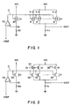
- Fig. 1 shows a D/A converter.
- This D/A converter is a current-segment type, designed to convert an n-bit digital signal to an analog signal, and, as is shown in Fig. 1, comprises 2 n - 1 variable current sources A, and 2 n - 1 switch devices S connected in series to sources A, respectively.
- variable current sources A and switch devices S form 2 n - 1 series circuits.
- Each of these series circuits is coupled between a power-supply terminal VCC and an output terminal VOUT.
- Switch devices S are selectively turned on or off by the outputs obtained by decoding the n-bit digital signal input to the D/A converter.
- Resistor R1 is connected at one end to variable current sources A, and changes the output current of each current source A into output voltage VOUT. Resistor R1 can, however, be omitted, in which case the output analog data of the D/A converter is then a current.
- the D/A converter further comprises control circuit 11 for controlling the output currents I0 of variable current sources A.
- Control circuit 11 comprises a variable current source AO, resistor R0, and voltage comparator C0.
- Variable current source A0 is of the same structure as variable current sources A, and along with resistor R0, is connected in series between power-supply terminal VCC and the ground. The potential V0 at the node of current source A0 and resistor R0 is applied to the first input terminal of voltage comparator C0, reference voltage VREF being applied to the second input terminal thereof.
- Fig. 2 shows the above D/A converter in greater detail.
- each switch device S is a P-type MOS transistor Q1
- each variable current source A is a P-type MOS transistor Q2
- the variable current source A0 of control circuit 11 is also a P-type MOS transistor, Q0.
- P-type MOS transistors Q0 and Q2 are both the same size and are formed on the same semiconductor chip.
- Outputs D1 to D2n ⁇ 1 ⁇ which have been obtained by decoding the n-bit digital signal, are supplied one to each of the gates of P-type MOS transistors Q1.
- the gate of P-type MOS transistor QO, and the gates of P-type MOS transistors Q2 are coupled to the output of comparator C0.
- P-type MOS transistor Q0 is used as a variable current source, a reference voltage is applied to the inverting input of comparator C0, with voltage V0 being applied to the non-inverting input thereof.
- the current I0 which flows through transistor Q0 can be controlled so as to maintain voltage VO equal to I-:eren-voltage VREF, even if the ambient temperature or the power-supply potential VCC change.
- V0 I0 ⁇ R0
- VOUT K ⁇ IO ⁇ R1
- VOUT k ⁇ R1 ⁇ VREF/RO where 0 ⁇ k ⁇ 2 n - 1.
- the D/A converter can output the voltage VOUT which is determined by reference voltage VREF and resistors R0 and R1 only, irrespective of the current I0 flowing through transistor Q0 of control circuit 11.
- the D/A converter can perform a stable digital-analog conversion, which is not influenced by variations in the ambient temperature or in power-supply voltage VCC.
- the full scale of the analog output can be easily changed to a desired value merely altering reference voltage VREF.
- variable current source A0 comprises two P-type MOS transistors, Q0' and Q0, connected in series.
- each variable current source A is made up of two P-type MOS transistors, Q2 and Q3, again connected in series.
- the gates of P-type MOS transistors Q0 and Q2 are coupled to the output of comparator C0, the gate and drain of P-type MOS transistor Q0' are connected to each other, and the node of the gate and drain of transistor Q0' is connected to the gates of P-type MOS transistors Q3.
- variable current source Since each variable current source has the specific structure described above, P-type MOS transistors Q0' and Q3 function as loads of P-type MOS transistors Q0 and Q2. Therefore, the variable current source can output a current more stable than the variable current source used in the D/A converter shown in Fig. 2, which includes only one transistor.
- Fig. 4 shows a D/A converter which has two switch devices, S and S , connected to each variable current source A. More specifically, one end of switch device S is coupled to variable current source A, and its other end is coupled to output terminal VOUT. One end of switch device S is coupled to variable current source A, and its other end to the ground.
- the 2 n - 1 decoded outputs obtained by decoding an input digital signal are supplied to the 2 n - 1 switch devices S, respectively, thereby turning on or off these switch devices.
- These 2 n - 1 decoded outputs are inverted by inverters (not shown) and supplied to 2 n - 1 switches S , respectively, thereby turning on or off these switch devices.
- each variable current source A is always connected to either output terminal VOUT or to the ground, regardless of the results of the decoding the digital signal.
- the D/A converter of Fig. 4 can operate at a speed higher than the D/A converter of the first embodiment, in which some time elapses until the output current of each variable current source increases to a predetermined value.
- Fig. 5 illustrates a D/A converter which is designed such that it divides an n-bit digital signal into two parts, the first part consisting of upper a-bits, and the second part consisting of lower b-bits, then converts these two parts of the digital signal to analog signals.
- this D/A converter comprises two D/A converting sections, 12 and 13. Section 12 is used to convert upper a-bits to an analog signal, while section 13 converts lower b-bits to an analog signal.
- D/A converting section 12 comprises 2 a - 1 switch devices S, 2 a - 1 variable current sources A, and control circuit 11a.
- Switch devices S are turned on or off by decoded upper a-bits.
- Variable current sources A are connected to switch devices S, respectively, the output current I0 of each source A being controlled by control circuit 11a.
- D/A converting section 13 comprises 2 b -1 switch devices S, 2 b - 1 variable current sources A, and control circuit 11b.
- Switch devices S are turned on or off by decoded lower b-bits.
- Variable current sources A of section 13 are also connected to switch devices S, respectively, the output current I1 of each of these sources A being controlled by control circuit 11b.
- Control circuit 11a comprises variable current 35 source A0, resistor R0, and voltage comparator C0.
- Control circuit 11b comprises variable current source A01, resistor R01, and voltage comparator C01. Resistor R01 is weighted such that its resistance is 2 b .R0. Except for this point, control circuit 11b is identical in structure to control circuit 11a.
- the output current I0 of each variable current source A of D/A converting section 12, and the output current I1 of each variable current source A of D/A converting section 13 are controlled to have values corresponding to reference voltage VREF.
- the D/A converter of third embodiment (Fig. 5) can, therefore, convert digital signals to analog signals with as high an accuracy as the D/A converters of the first and second embodiments.
- Fig. 6 shows a further D/A converter.
- this D/A converter divides an n-bit digital signal into two parts, the first consisting of upper a-bits, and the second part consisting of lower b-bits, and converts the two parts of the digital signal to analog signals by means of D/A converting sections 12 and 13.
- This D/A converter is different in that circuit 11b comprises 2 b current sources A01 connected in parallel, instead of weighting resistor R01.
- control circuit 11b which is designed to control the output current I1 of each variable current source of D/A converting section 13, comprises 2 b variable current sources A01, resistor R01, and voltage comparator C01.
- Current sources A01 are of the same structure as variable current sources A, and resistor R01 is identical to resistor R0.
- Variable current sources A01 are connected in parallel between power-supply terminal VCC and resistor R01, and are controlled by the output of voltage comparator C01, thereby to provide a current.
- control circuit 11b can set output current I1 of each variable current source A of D/A converting section 13 at a predetermined value.
- Variable current sources A, A0, and A01 can each comprise one P-type MOS transistor, as is shown in Fig. 2, or two p-type MOS transistors, as is shown in Fig. 3. Alternatively, they can each be formed of one or two N-type MOS transistors, or of one or two bipolar transistors.
- output resistor R1 can be dispensed with, in which case, each analog signal is output in the form of a current, thereby achieving the same advantages as in these converters described above.
Description
- The present invention relates to a digital-to-analog converter for converting digital signals to analog signals, and more particularly, to a digital-analog converter for use in an apparatus, such as a video signal-processing apparatus, in which signals must be processed at high speed.
- Most video signal-processing apparatuses includes a high-speed D/A (digital-analog) current-segment type converter. This type of converter comprises a plurality of constant current sources each having a switch connected thereto. When the D/A converter is designed to convert an n-bit digital signal to an anaiog signal, it then comprises 2n - i current sources and 2n - 1 switches. This is because an n-bit digital signal is changed into 2n decoded outputs, and the current supply from all constant current sources must be stopped when all bits of the input digital signal are "0".
- The 2n - 1 switches are selectively turned on in accordance with the results of the decoding of the digital signal. Therefore, the value of the analog output of the current-segment type D/A converter increases by the output current of one current source when the content of the input digital signal increases by one.
- The full scale of the analog output of such a D/A converter, i.e., the output range from the minimum value to the maximum value, is determined by the structure of the device, or the output current values of the current sources. Once the D/A converter has been manufactured, its full-scale value cannot be altered. Consequently, the use of the D/A converter is limited.
- Since the output current of each current source changes with variations in the ambient temperature and/or the power-supply voltage, the analog output of this type of D/A converter therefore tends to be unstable during operation. As a result, this D/A converter can hardly achieve a high-accuracy D/A conversion of signals.
- Prior art document DE-A-28 03 099 discloses a digital-to-analog converter having features similar to those included in the precharacterizing part of
claim 1. - It is an object of the present invention to provide a D/A converter whose output full-scale value can be easily altered, whose D/A-conversion accuracy is not influenced by variations in the ambient temperature and/or the power-supply voltage, and which can therefore be versatile and accomplish high-accuracy D/A conversion of signals.
- To solve this object the present invention provides a digital-to-analog converter as specified in
claim 1. - A digital-analog converter comprises a digital-analog converting circuit including a plurality of serial circuits, each of which has a switch device and a first variable current source capable of supplying currents of different values, a second variable current source of the same structure as the first variable current source, a voltage-generating element for generating a voltage corresponding to the output current of the second variable current source, and a comparator for comparing the output voltage of the voltage-generating element with a reference voltage. The serial circuits are connected in series to a plurality of current paths, respectively. These current paths are provided between a power-supply potential terminal and an output terminal. The digital-analog converting circuit converts an input digital signal to an analog signal as the switch devices are selectively turned on in accordance with the input digital signal. The second variable current source is connected at its one terminal to the power-supply potential terminal. The difference between the voltages compared by the comparator determines the level of the output currents of the first and second variable current sources.
- Since the output of the comparator controls the output current of the second variable current source such that the voltage-generating element generates a voltage equal to the reference voltage, the output current of the second variable current source is sufficiently stable. Such the first variable current source is identical in structure to the second variable current source, the output current of the first variable current source therefore corresponds to the reference voltage. The D/A converter of this invention can present an analog output which is not influenced by variations in the ambient temperature or in the power-supply voltage, and which is therefore stable. When the level of the reference voltage is changed, the output current of the first variable current source changes proportionally. Thus, the full scale of the analog output of the D/A converter can be easily changed to any desired value.
- This invention can be more fully understood from the following detailed description when taken in conjunction with the accompanying drawings, in which:
- Fig. 1 is a circuit diagram showing a digital-analog converter;
- Fig. 2 is a circuit diagram illustrating the digital-analog converter of Fig. 1 in greater detail, in particular, showing the switch devices and the current sources of the converter;
- Fig. 3 is a circuit diagram showing a modification of the digital-analog converter shown in Fig. 2 according to an embodiment of the present invention;
- Fig. 4 is a circuit diagram representing a further digital-analog converter;
- Fig. 5 is a circuit diagram showing a further digital-analog converter; and
- Fig. 6 is a circuit diagram illustrating a further digital-analog converter.
- Fig. 1 shows a D/A converter. This D/A converter is a current-segment type, designed to convert an n-bit digital signal to an analog signal, and, as is shown in Fig. 1, comprises 2n - 1 variable current sources A, and 2n - 1 switch devices S connected in series to sources A, respectively. Thus, variable current sources A and switch devices S form 2n - 1 series circuits. Each of these series circuits is coupled between a power-supply terminal VCC and an output terminal VOUT. Switch devices S are selectively turned on or off by the outputs obtained by decoding the n-bit digital signal input to the D/A converter. Resistor R1 is connected at one end to variable current sources A, and changes the output current of each current source A into output voltage VOUT. Resistor R1 can, however, be omitted, in which case the output analog data of the D/A converter is then a current. The D/A converter further comprises
control circuit 11 for controlling the output currents I0 of variable current sources A. -
Control circuit 11 comprises a variable current source AO, resistor R0, and voltage comparator C0. Variable current source A0 is of the same structure as variable current sources A, and along with resistor R0, is connected in series between power-supply terminal VCC and the ground. The potential V0 at the node of current source A0 and resistor R0 is applied to the first input terminal of voltage comparator C0, reference voltage VREF being applied to the second input terminal thereof. - Fig. 2 shows the above D/A converter in greater detail. As is illustrated in this figure, each switch device S is a P-type MOS transistor Q1, each variable current source A is a P-type MOS transistor Q2, and the variable current source A0 of
control circuit 11 is also a P-type MOS transistor, Q0. P-type MOS transistors Q0 and Q2 are both the same size and are formed on the same semiconductor chip. Outputs D₁ to D₂n₋₁ʹ which have been obtained by decoding the n-bit digital signal, are supplied one to each of the gates of P-type MOS transistors Q1. The gate of P-type MOS transistor QO, and the gates of P-type MOS transistors Q2 are coupled to the output of comparator C0. Since P-type MOS transistor Q0 is used as a variable current source, a reference voltage is applied to the inverting input of comparator C0, with voltage V0 being applied to the non-inverting input thereof. As a result, the current I0 which flows through transistor Q0 can be controlled so as to maintain voltage VO equal to I-:eren-voltage VREF, even if the ambient temperature or the power-supply potential VCC change. Since

When k P-type MOS transistors Q1 are turned on in accordance with the outputs obtained by decoding the digital signal, output voltage VOUT is given as:

Thus:

where 0 ≦ k ≦ 2n - 1. - Therefore, the D/A converter can output the voltage VOUT which is determined by reference voltage VREF and resistors R0 and R1 only, irrespective of the current I0 flowing through transistor Q0 of
control circuit 11. In other words, the D/A converter can perform a stable digital-analog conversion, which is not influenced by variations in the ambient temperature or in power-supply voltage VCC. Furthermore, the full scale of the analog output can be easily changed to a desired value merely altering reference voltage VREF. - Fig. 3 shows an embodiment of the present invention which is a modification of the D/A converter shown in Fig. 2. The D/A converter of Fig. 3 differs from the converter of Fig. 2 in two principal respects. First, variable current source A0 comprises two P-type MOS transistors, Q0' and Q0, connected in series. Secondly, each variable current source A is made up of two P-type MOS transistors, Q2 and Q3, again connected in series. The gates of P-type MOS transistors Q0 and Q2 are coupled to the output of comparator C0, the gate and drain of P-type MOS transistor Q0' are connected to each other, and the node of the gate and drain of transistor Q0' is connected to the gates of P-type MOS transistors Q3.
- Since each variable current source has the specific structure described above, P-type MOS transistors Q0' and Q3 function as loads of P-type MOS transistors Q0 and Q2. Therefore, the variable current source can output a current more stable than the variable current source used in the D/A converter shown in Fig. 2, which includes only one transistor.
- Fig. 4 shows a D/A converter which has two switch devices, S and
S , connected to each variable current source A. More specifically, one end of switch device S is coupled to variable current source A, and its other end is coupled to output terminal VOUT. One end of switch deviceS is coupled to variable current source A, and its other end to the ground. The 2n - 1 decoded outputs obtained by decoding an input digital signal are supplied to the 2n - 1 switch devices S, respectively, thereby turning on or off these switch devices. These 2n - 1 decoded outputs are inverted by inverters (not shown) and supplied to 2n - 1 switchesS , respectively, thereby turning on or off these switch devices. Hence, each variable current source A is always connected to either output terminal VOUT or to the ground, regardless of the results of the decoding the digital signal. The D/A converter of Fig. 4 can operate at a speed higher than the D/A converter of the first embodiment, in which some time elapses until the output current of each variable current source increases to a predetermined value. - Fig. 5 illustrates a D/A converter which is designed such that it divides an n-bit digital signal into two parts, the first part consisting of upper a-bits, and the second part consisting of lower b-bits, then converts these two parts of the digital signal to analog signals. As is shown in Fig. 5, this D/A converter comprises two D/A converting sections, 12 and 13.
Section 12 is used to convert upper a-bits to an analog signal, whilesection 13 converts lower b-bits to an analog signal. - D/A converting
section 12 comprises 2a - 1 switch devices S, 2a - 1 variable current sources A, and controlcircuit 11a. Switch devices S are turned on or off by decoded upper a-bits. Variable current sources A are connected to switch devices S, respectively, the output current I0 of each source A being controlled bycontrol circuit 11a. - Similarly, D/A converting
section 13 comprises 2b -1 switch devices S, 2b - 1 variable current sources A, andcontrol circuit 11b. Switch devices S are turned on or off by decoded lower b-bits. Variable current sources A ofsection 13 are also connected to switch devices S, respectively, the output current I1 of each of these sources A being controlled bycontrol circuit 11b. -
Control circuit 11a comprises variable current 35 source A0, resistor R0, and voltage comparator C0.Control circuit 11b comprises variable current source A01, resistor R01, and voltage comparator C01. Resistor R01 is weighted such that its resistance is 2b.R0. Except for this point,control circuit 11b is identical in structure to controlcircuit 11a. - The output current I0 of each variable current source A of D/A converting
section 12, and the output current I1 of each variable current source A of D/A convertingsection 13 are controlled to have values corresponding to reference voltage VREF. The D/A converter of third embodiment (Fig. 5) can, therefore, convert digital signals to analog signals with as high an accuracy as the D/A converters of the first and second embodiments. In addition, it is possible with the D/A converter of the third embodiment to set the full scale of analog output to a desired value, merely by changing reference voltage VREF. - Fig. 6 shows a further D/A converter. Like the D/A converter shown in Fig. 5, this D/A converter divides an n-bit digital signal into two parts, the first consisting of upper a-bits, and the second part consisting of lower b-bits, and converts the two parts of the digital signal to analog signals by means of D/
A converting sections circuit 11b comprises 2b current sources A01 connected in parallel, instead of weighting resistor R01. - More precisely,
control circuit 11b, which is designed to control the output current I1 of each variable current source of D/A convertingsection 13, comprises 2b variable current sources A01, resistor R01, and voltage comparator C01. Current sources A01 are of the same structure as variable current sources A, and resistor R01 is identical to resistor R0. Variable current sources A01 are connected in parallel between power-supply terminal VCC and resistor R01, and are controlled by the output of voltage comparator C01, thereby to provide a current. Hence,control circuit 11b can set output current I1 of each variable current source A of D/A convertingsection 13 at a predetermined value. - Variable current sources A, A0, and A01 can each comprise one P-type MOS transistor, as is shown in Fig. 2, or two p-type MOS transistors, as is shown in Fig. 3. Alternatively, they can each be formed of one or two N-type MOS transistors, or of one or two bipolar transistors.
- Furthermore, in the above converters, output resistor R1 can be dispensed with, in which case, each analog signal is output in the form of a current, thereby achieving the same advantages as in these converters described above.
Claims (3)
- A digital-to-analog converter for converting a digital signal to an analog signal, comprising:
a digital-to-analog converting circuit connected to receive a digital signal (D1), and including a plurality of serial circuits each of which has a switch device (Q1) and a first variable current source (Q2, Q3) which are connected in series between a power-supply potential terminal (VCC) and an output terminal (VOUT), the conduction states of said switch devices (Q1) being determined by the digital signal (D1), whereby said output terminal (VOUT) is supplied with an analog value corresponding to the number of switch devices (Q1) which are in a conductive state;
a second variable current source (Q0, Q0') connected, at one end, to said power-supply potential terminal (VCC);
voltage-generating means (RO) for generating a voltage corresponding to a current output by said second variable current source (Q0, Q0'); and
comparator means (CO) for comparing the voltage generated by said voltage-generating means (RO) with a reference voltage (VREF), and controlling the output currents of said first variable current sources (Q2, Q3) add the output current of said second variable current source (Q0, Q0') in accordance with the difference between the reference voltage (VREF) and the output voltage of said voltage-generating means (R0),
characterized in that
said first and second variable current sources (Q2, Q3; Q0, Q0') each include two serially connected MOS transistors, all said MOS transistors being formed on the same semiconductor chip and being the same size, the gate of the first MOS transistor (Q2) of each first current variable source (Q2, Q3) and the gate of the first MOS transistor (Q0) of the second variable current source (Q0, Q0') being coupled to the output of said comparator means (C0), the gate and drain of the second MOS transistor (Q0') of said second variable current source (Q0, Q0') being coupled to each other, and the gate of the second MOS transistor (Q3) of each first variable current source (Q2, Q3) being connected to the node of the gate and drain of the second MOS transistor (Q0') of said second variable current source (Q0, Q0'). - A digital-to-analog converter according to claim 1, characterized in that said switch devices (Q1) each include a P-type MOS transistor (Q1) whose gate is connected to receive one bit of the decoded digital signal (D1).
- A digital-to-analog converter according to claim 1 or 2, characterized in that said reference voltage has a value corresponding to the full scale of the analog output supplied from said output terminal (VOUT).
Applications Claiming Priority (2)
| Application Number | Priority Date | Filing Date | Title |
|---|---|---|---|
| JP47734/87 | 1987-03-04 | ||
| JP62047734A JPH0810832B2 (en) | 1987-03-04 | 1987-03-04 | Digital-to-analog converter |
Publications (3)
| Publication Number | Publication Date |
|---|---|
| EP0281116A2 EP0281116A2 (en) | 1988-09-07 |
| EP0281116A3 EP0281116A3 (en) | 1991-07-03 |
| EP0281116B1 true EP0281116B1 (en) | 1994-08-10 |
Family
ID=12783568
Family Applications (1)
| Application Number | Title | Priority Date | Filing Date |
|---|---|---|---|
| EP88103205A Expired - Lifetime EP0281116B1 (en) | 1987-03-04 | 1988-03-02 | Digital-to-analog converter |
Country Status (5)
| Country | Link |
|---|---|
| US (1) | US4827260A (en) |
| EP (1) | EP0281116B1 (en) |
| JP (1) | JPH0810832B2 (en) |
| KR (1) | KR900008821B1 (en) |
| DE (1) | DE3850982T2 (en) |
Cited By (1)
| Publication number | Priority date | Publication date | Assignee | Title |
|---|---|---|---|---|
| CN104298287A (en) * | 2013-07-17 | 2015-01-21 | 联发科技(新加坡)私人有限公司 | Current correcting method and device and resistance correcting method and device |
Families Citing this family (41)
| Publication number | Priority date | Publication date | Assignee | Title |
|---|---|---|---|---|
| JPH01220524A (en) * | 1988-02-26 | 1989-09-04 | Nec Corp | D/a converter |
| JPH01277027A (en) * | 1988-04-28 | 1989-11-07 | Toshiba Corp | Digital/analog converting circuit |
| JP2597712B2 (en) * | 1989-05-22 | 1997-04-09 | 株式会社東芝 | Digital to analog converter |
| US5001481A (en) * | 1990-01-30 | 1991-03-19 | David Sarnoff Research Center, Inc. | MOS transistor threshold compensation circuit |
| JPH0775322B2 (en) * | 1990-02-22 | 1995-08-09 | 富士通株式会社 | Semiconductor integrated circuit device |
| US5012178A (en) * | 1990-03-19 | 1991-04-30 | Triquint Semiconductor, Inc. | Low noise DAC current source topology |
| US5017919A (en) * | 1990-06-06 | 1991-05-21 | Western Digital Corporation | Digital-to-analog converter with bit weight segmented arrays |
| US5001482A (en) * | 1990-06-11 | 1991-03-19 | International Business Machines Corporation | BiCMOS digital-to-analog converter for disk drive digital recording channel architecture |
| JPH0470215A (en) * | 1990-07-11 | 1992-03-05 | Sony Corp | D/a converter |
| US5243239A (en) * | 1991-01-22 | 1993-09-07 | Information Storage Devices, Inc. | Integrated MOSFET resistance and oscillator frequency control and trim methods and apparatus |
| WO1992014336A1 (en) * | 1991-02-01 | 1992-08-20 | Analog Devices, Incorporated | System for developing crt color-intensity control signals in high resolution crt display equipment |
| US5254994A (en) * | 1991-03-06 | 1993-10-19 | Kabushiki Kaisha Toshiba | Current source cell use in current segment type D and A converter |
| US5293166A (en) * | 1992-03-31 | 1994-03-08 | Vlsi Technology, Inc. | Digital-to-analog converter and bias compensator therefor |
| EP0621729B1 (en) * | 1993-04-22 | 1998-02-25 | Siemens Aktiengesellschaft | Device for display of a first picture in a second picture on a screen |
| US5594441A (en) * | 1994-12-30 | 1997-01-14 | Psc, Inc. | D/A converter with constant gate voltage |
| TW331679B (en) * | 1995-12-22 | 1998-05-11 | Thomson Multimedia Sa | Analog-to-digital converter. |
| KR100487495B1 (en) * | 1997-08-26 | 2005-08-24 | 삼성전자주식회사 | Digital-analog converter |
| US6140860A (en) * | 1997-12-31 | 2000-10-31 | Intel Corporation | Thermal sensing circuit |
| US6154067A (en) * | 1998-08-05 | 2000-11-28 | Adaptec, Inc. | Methods of and apparatus for monitoring the termination status of a SCSI bus |
| JP3246498B2 (en) | 1999-11-30 | 2002-01-15 | ヤマハ株式会社 | Digital / analog converter |
| US6377197B1 (en) * | 2000-08-15 | 2002-04-23 | Nokia Mobile Phones Ltd. | DAC gain compensation for temperature and process variations |
| DE10053914C2 (en) * | 2000-10-31 | 2003-05-22 | Infineon Technologies Ag | Digital / analog converter with programmable amplification |
| KR100495500B1 (en) * | 2000-12-14 | 2005-06-17 | 매그나칩 반도체 유한회사 | Digital to analog converter |
| JP4500439B2 (en) * | 2000-12-22 | 2010-07-14 | 川崎マイクロエレクトロニクス株式会社 | Semiconductor device |
| JP4662698B2 (en) * | 2003-06-25 | 2011-03-30 | ルネサスエレクトロニクス株式会社 | Current source circuit and current setting method |
| TWI292146B (en) * | 2003-08-13 | 2008-01-01 | Via Tech Inc | Display controller and related method for calibrating display driving voltages accordign to input resistance of a monitor |
| DE602005017260D1 (en) * | 2005-07-27 | 2009-12-03 | Verigy Pte Ltd Singapore | Digital analog conversion in which the outputs of several digital-to-analog converters are added up |
| US8228096B2 (en) * | 2007-03-02 | 2012-07-24 | Kawasaki Microelectronics, Inc. | Circuit and method for current-mode output driver with pre-emphasis |
| JP5166898B2 (en) * | 2008-02-04 | 2013-03-21 | 三洋半導体株式会社 | Output value adjustment circuit and current value adjustment circuit |
| US10826525B1 (en) | 2018-04-17 | 2020-11-03 | Ali Tasdighi Far | Nonlinear data conversion for multi-quadrant multiplication in artificial intelligence |
| US10848167B1 (en) | 2018-04-17 | 2020-11-24 | Ali Tasdighi Far | Floating current-mode digital-to-analog-converters for small multipliers in artificial intelligence |
| US10862501B1 (en) | 2018-04-17 | 2020-12-08 | Ali Tasdighi Far | Compact high-speed multi-channel current-mode data-converters for artificial neural networks |
| US10789046B1 (en) | 2018-04-17 | 2020-09-29 | Ali Tasdighi Far | Low-power fast current-mode meshed multiplication for multiply-accumulate in artificial intelligence |
| US11016732B1 (en) | 2018-04-17 | 2021-05-25 | Ali Tasdighi Far | Approximate nonlinear digital data conversion for small size multiply-accumulate in artificial intelligence |
| US10884705B1 (en) | 2018-04-17 | 2021-01-05 | Ali Tasdighi Far | Approximate mixed-mode square-accumulate for small area machine learning |
| US11144316B1 (en) | 2018-04-17 | 2021-10-12 | Ali Tasdighi Far | Current-mode mixed-signal SRAM based compute-in-memory for low power machine learning |
| US10804925B1 (en) | 2018-04-17 | 2020-10-13 | Ali Tasdighi Far | Tiny factorized data-converters for artificial intelligence signal processing |
| US10832014B1 (en) | 2018-04-17 | 2020-11-10 | Ali Tasdighi Far | Multi-quadrant analog current-mode multipliers for artificial intelligence |
| US10819283B1 (en) | 2019-06-04 | 2020-10-27 | Ali Tasdighi Far | Current-mode analog multipliers using substrate bipolar transistors in CMOS for artificial intelligence |
| US11610104B1 (en) | 2019-12-30 | 2023-03-21 | Ali Tasdighi Far | Asynchronous analog accelerator for fully connected artificial neural networks |
| US11615256B1 (en) | 2019-12-30 | 2023-03-28 | Ali Tasdighi Far | Hybrid accumulation method in multiply-accumulate for machine learning |
Family Cites Families (6)
| Publication number | Priority date | Publication date | Assignee | Title |
|---|---|---|---|---|
| FR1572409A (en) * | 1968-04-24 | 1969-06-27 | ||
| GB1266886A (en) * | 1968-10-03 | 1972-03-15 | ||
| DE2803099C3 (en) * | 1978-01-25 | 1986-07-10 | Hans-Ulrich 5810 Witten Post | Digital-to-analog converter in integrated circuit technology |
| US4482887A (en) * | 1979-02-15 | 1984-11-13 | International Business Machines Corporation | Integrated weighted current digital to analog converter |
| JPS56131227A (en) * | 1980-03-19 | 1981-10-14 | Hitachi Ltd | Negative feedback circuit for reference voltage of da converter |
| US4523182A (en) * | 1983-01-10 | 1985-06-11 | Advanced Micro Devices, Inc. | PROM trimmed digital-to-analog converter |
-
1987
- 1987-03-04 JP JP62047734A patent/JPH0810832B2/en not_active Expired - Fee Related
-
1988
- 1988-02-29 US US07/162,264 patent/US4827260A/en not_active Expired - Lifetime
- 1988-03-02 EP EP88103205A patent/EP0281116B1/en not_active Expired - Lifetime
- 1988-03-02 DE DE3850982T patent/DE3850982T2/en not_active Expired - Fee Related
- 1988-03-04 KR KR1019880002229A patent/KR900008821B1/en not_active IP Right Cessation
Non-Patent Citations (1)
| Title |
|---|
| ANALOG DEVICES: DATA ACQUISITION PRODUCTS CATALOG SUPPLEMENT, 1979, pages S143 and S146 * |
Cited By (2)
| Publication number | Priority date | Publication date | Assignee | Title |
|---|---|---|---|---|
| CN104298287A (en) * | 2013-07-17 | 2015-01-21 | 联发科技(新加坡)私人有限公司 | Current correcting method and device and resistance correcting method and device |
| CN104298287B (en) * | 2013-07-17 | 2016-04-20 | 联发科技(新加坡)私人有限公司 | Current correction method and device and resistance bearing calibration and device |
Also Published As
| Publication number | Publication date |
|---|---|
| KR880012020A (en) | 1988-10-31 |
| KR900008821B1 (en) | 1990-11-30 |
| DE3850982D1 (en) | 1994-09-15 |
| EP0281116A2 (en) | 1988-09-07 |
| US4827260A (en) | 1989-05-02 |
| EP0281116A3 (en) | 1991-07-03 |
| DE3850982T2 (en) | 1994-12-15 |
| JPS63215224A (en) | 1988-09-07 |
| JPH0810832B2 (en) | 1996-01-31 |
Similar Documents
| Publication | Publication Date | Title |
|---|---|---|
| EP0281116B1 (en) | Digital-to-analog converter | |
| US5801655A (en) | Multi-channel D/A converter utilizing a coarse D/A converter and a fine D/A converter | |
| US5585795A (en) | D/A converter including output buffer having a controllable offset voltage | |
| US5936566A (en) | Auto-reference pseudo-flash analog to digital converter | |
| EP3614227B1 (en) | Dual loop low dropout regulator system | |
| US5043730A (en) | Digital-analog conversion circuit with application of voltage biasing for distortion stabilization | |
| EP0466145B1 (en) | D/A converter | |
| US6724333B1 (en) | Digital-to-analog converter | |
| US5568146A (en) | Digital/analog converter | |
| JPH0519848B2 (en) | ||
| JPS62155623A (en) | Digital-analog converter | |
| JP3067903B2 (en) | Analog / digital converter | |
| JP2002076895A (en) | Current cell type digital/analog converter system | |
| JP3551200B2 (en) | Digital / analog conversion circuit | |
| US4814740A (en) | Glitch occurence prevention circuit for a digital/analog converter | |
| JP3090099B2 (en) | D / A converter | |
| KR0137765B1 (en) | Current split circuit having a digital to analog converter | |
| JPH04138725A (en) | D/a converter | |
| JP2000201076A (en) | A/d converter | |
| JPH03145330A (en) | Latching comparator circuit | |
| CN117811584A (en) | Digital-to-analog converter | |
| JP2976447B2 (en) | D / A converter | |
| JPH04418B2 (en) | ||
| KR19990030332A (en) | Two-Stage Analog-to-Digital Converter Circuit Operates at Low Voltages | |
| KR100517543B1 (en) | Ad/da converter with reference voltage control function |
Legal Events
| Date | Code | Title | Description |
|---|---|---|---|
| PUAI | Public reference made under article 153(3) epc to a published international application that has entered the european phase |
Free format text: ORIGINAL CODE: 0009012 |
|
| 17P | Request for examination filed |
Effective date: 19880330 |
|
| AK | Designated contracting states |
Kind code of ref document: A2 Designated state(s): DE FR GB |
|
| PUAL | Search report despatched |
Free format text: ORIGINAL CODE: 0009013 |
|
| AK | Designated contracting states |
Kind code of ref document: A3 Designated state(s): DE FR GB |
|
| RHK1 | Main classification (correction) |
Ipc: H03M 1/06 |
|
| 17Q | First examination report despatched |
Effective date: 19930708 |
|
| GRAA | (expected) grant |
Free format text: ORIGINAL CODE: 0009210 |
|
| AK | Designated contracting states |
Kind code of ref document: B1 Designated state(s): DE FR GB |
|
| REF | Corresponds to: |
Ref document number: 3850982 Country of ref document: DE Date of ref document: 19940915 |
|
| ET | Fr: translation filed | ||
| PLBE | No opposition filed within time limit |
Free format text: ORIGINAL CODE: 0009261 |
|
| STAA | Information on the status of an ep patent application or granted ep patent |
Free format text: STATUS: NO OPPOSITION FILED WITHIN TIME LIMIT |
|
| 26N | No opposition filed | ||
| PGFP | Annual fee paid to national office [announced via postgrant information from national office to epo] |
Ref country code: DE Payment date: 19980306 Year of fee payment: 11 |
|
| PGFP | Annual fee paid to national office [announced via postgrant information from national office to epo] |
Ref country code: FR Payment date: 19980310 Year of fee payment: 11 |
|
| PG25 | Lapsed in a contracting state [announced via postgrant information from national office to epo] |
Ref country code: FR Free format text: LAPSE BECAUSE OF NON-PAYMENT OF DUE FEES Effective date: 19991130 |
|
| REG | Reference to a national code |
Ref country code: FR Ref legal event code: ST |
|
| PG25 | Lapsed in a contracting state [announced via postgrant information from national office to epo] |
Ref country code: DE Free format text: LAPSE BECAUSE OF NON-PAYMENT OF DUE FEES Effective date: 20000101 |
|
| REG | Reference to a national code |
Ref country code: GB Ref legal event code: IF02 |
|
| PGFP | Annual fee paid to national office [announced via postgrant information from national office to epo] |
Ref country code: GB Payment date: 20070228 Year of fee payment: 20 |
|
| REG | Reference to a national code |
Ref country code: GB Ref legal event code: PE20 |
|
| PG25 | Lapsed in a contracting state [announced via postgrant information from national office to epo] |
Ref country code: GB Free format text: LAPSE BECAUSE OF EXPIRATION OF PROTECTION Effective date: 20080301 |