EP0280869A2 - Laser-Lumineszenz-Monitor für Materialdickenprozesse - Google Patents
Laser-Lumineszenz-Monitor für Materialdickenprozesse Download PDFInfo
- Publication number
- EP0280869A2 EP0280869A2 EP88101092A EP88101092A EP0280869A2 EP 0280869 A2 EP0280869 A2 EP 0280869A2 EP 88101092 A EP88101092 A EP 88101092A EP 88101092 A EP88101092 A EP 88101092A EP 0280869 A2 EP0280869 A2 EP 0280869A2
- Authority
- EP
- European Patent Office
- Prior art keywords
- energy
- material layer
- thickness
- detecting
- bandgap
- Prior art date
- Legal status (The legal status is an assumption and is not a legal conclusion. Google has not performed a legal analysis and makes no representation as to the accuracy of the status listed.)
- Granted
Links
Images
Classifications
-
- G—PHYSICS
- G01—MEASURING; TESTING
- G01B—MEASURING LENGTH, THICKNESS OR SIMILAR LINEAR DIMENSIONS; MEASURING ANGLES; MEASURING AREAS; MEASURING IRREGULARITIES OF SURFACES OR CONTOURS
- G01B11/00—Measuring arrangements characterised by the use of optical techniques
- G01B11/02—Measuring arrangements characterised by the use of optical techniques for measuring length, width or thickness
- G01B11/06—Measuring arrangements characterised by the use of optical techniques for measuring length, width or thickness for measuring thickness ; e.g. of sheet material
- G01B11/0616—Measuring arrangements characterised by the use of optical techniques for measuring length, width or thickness for measuring thickness ; e.g. of sheet material of coating
- G01B11/0658—Measuring arrangements characterised by the use of optical techniques for measuring length, width or thickness for measuring thickness ; e.g. of sheet material of coating with measurement of emissivity or reradiation
Definitions
- the present invention relates generally to a means and a method for processing semiconductor and other materials, and more particularly, to a means and a method for monitoring the change in thickness of a thin material layer during a thickness-changing operation.
- reactive ion etching or plasma etching is now typically used to delineate fine line patterns and trenches in thin films of either insulators, semiconductors, or metals by means of the removal of portions of these films in a plasma discharge.
- the wafer to be etched is placed in a plasma chamber into which a gas mixture is directed at a reduced pressure.
- reactive species are generated from the feed gas by processes such as dissociative or impact ionization.
- Portions of the thin film are removed by chemical reaction between the reactive species and the film, as well as by bombardment of the film by ions present in the plasma.
- the gaseous reaction products formed by the chemical reactions and the ion bombardment of the film are continuously removed from the chamber using a vacuum pump.
- a majority chemical species from the layer being etched enters the etching plasma and is observed by monitoring a relevant spectral line for that majority species as the etching process consumes the layer being etched.
- the time to terminate the process is inferred from changes in the intensity of this monitored majority species spectral line.
- monitoring of the majority species from the etched layer will not provide a determination of the etch endpoint.
- a similar problem is encountered when techniques are utilized to compensate for etch loading non-uniformities.
- an aluminum film on a wafer is many times etched by disposing the wafer on a high purity aluminum target to thereby prevent a sudden large excess of etching species near the end of the etch process which would cause an attendant undercutting of the aluminum film.
- this aluminum target prevents the determination of the etch endpoint by monitoring the majority aluminum species.
- This problem is especially acute for the etching of GaAs down to a layer of AlGaAs.
- Optical emission or laser induced fluorescence of atomic aluminum present in the etching plasma is not sensitive enough to detect the subtle aluminum concentration change as the interface between the GaAs and AlGaAs layers is reached, because most RIE reactor chambers are made of aluminum. The aluminum sputtered from the chamber walls during the RIE process essentially buries any such aluminum concentration change.
- the invention as claimed is intended to remedy the above-described drawbacks in thickness-changing process monitoring.
- the advantage offered by the present invention is that it allows accurate monitoring of a thickness-changing-changing process.
- the invention permits the monitoring of the deposition of a very thin layer of material over a second different material.
- the invention permits the monitoring of material thickness reduction down to a very thin layer above a second different material.
- the invention permits the accurate monitoring of the etch-through from a first material to a second different material.
- the present invention comprises a method and an apparatus for monitoring a change of thickness of a first material layer having a first bandgap wavelength energy, with the first material layer for disposal over a second material layer on a wafer, wherein the second material layer has a second different bandgap wavelength energy and wherein at least one of the first and second materials has a direct bandgap.
- the apparatus comprises : means for holding the wafer and for changing the thickness of the first material layer at a particular location over the second material layer, means for generating a beam of energy of an intensity and wavelength sufficient to pump the at least one bandgap material layer with its direct bandgap wavelength energy to a higher energy state, means for directing the beam of energy to impinge at an angle onto the surface and to penetrate said wafer at the location where the first material thickness is being changed; and means for detecting induced luminescence from the at least one direct bandgap material layer to determine when to stop the thickness changing means.
- the apparatus further includes means for varying the angle at which the beam of energy impinges onto the surface of the wafer, to thereby vary the depth to which the beam penetrates into the wafer.
- the thickness changing means comprises means for depositing the first material layer onto the second material layer.
- the thickness changing means comprises means for reducing the thickness of an existing first material layer.
- the energy beam generating means may include means for generating an energy beam that includes energy of an intensity and wavelength sufficient to pump the first material layer with a first direct bandgap wavelength energy to a higher energy state; and wherein the detecting means includes means for detecting the induced luminescence from the pumped first material layer.
- the energy beam generating means may include means for generating an energy beam that includes energy of an intensity and a wavelength sufficient to pump the second material layer with a second direct bandgap wavelength energy to a higher energy state; and wherein the detecting means includes means for detecting the induced luminescence from the pumped second material layer.
- the detecting means may include means for changing the operation of the thickness reducing means a predetermined time after either the second material induced luminescence has been detected above a predetermined threshold, or after the first material induced luminescence is no longer detected above a predetermined threshold, or some combination of the two.
- the first layer is GaAs
- the second material layer is AlGaAs.
- the present invention further includes the method for monitoring a change in thickness of a first material layer with a first bandgap energy, with the first material layer for disposal over a second material layer formed on a wafer, with the second material layer having a second different bandgap energy, wherein at least one of the first and second materials has a direct bandgap.
- the Figure discloses one embodiment of the present invention.
- the present invention discloses an apparatus and a method for monitoring a change of thickness of a first material layer having a first bandgap wavelength energy, with the first material layer for disposal over a second material layer on a wafer, which second material wafer has a second different bandgap wavelength energy, wherein at least one of the first and second materials has a direct bandgap.
- the present invention is based on the monitoring of laser-induced luminescence of this at least one direct bandgap material layer, either by itself, or in combination with the laser-induced luminescence of the other material layer. If both the first and second material layers have direct bandgaps, then their respective luminescence peaks must be separated in the optical spectrum.
- the phrase “thickness-changing” is meant to refer to apparatus and processes which both increase the thickness of a given layer to a desired thickness, and also to apparatus and processes which reduce the thickness of the desired layer to either a predetermined thickness or to zero thickness.
- the phrase “thickness-changing” thus encompasses a variety of processes including deposition, and etching and ion milling.
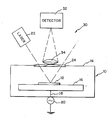
- the thickness-changing means 10 comprises a reactive ion etching chamber 14, which includes an electrode 16 connected via line 18 to an external RF power supply 20.
- the wafer 12 to be etched is disposed on one surface of the electrode 16.
- a typical reactive ion etching apparatus of the type shown is described in 3rd International Symposium on Dry Etching, Cachan, France, December l986.
- the etching chamber 14 is typically pumped down to a vacuum equal to or less and than 5 ⁇ 10-6 torr.
- the chamber 14 is then backfilled with a gas mixture appropriate to form a desired etching plasma for the layer on the wafer to be etched.
- a gas mixture of 18m torr of CCl2F2 and 18m torr of He is backfilled into the chamber 14.
- reactive species are generated from the backfilled gas.
- Portions of the first layer of GaAs are then removed by the chemical reaction between the reactive species and the GaAs, as well as by bombardment of the film by ions present in the plasma.
- the above-described reactive ion etching process is well known in the art.
- means 22 for generating a beam of energy of an intensity and wavelength sufficient to pump the at least one direct bandgap material layer to a higher energy state is provided.
- this beam generating means 22 is implemented by a laser which is disposed to direct its laser beam of energy to impinge at an angle onto the surface and to penetrate the wafer at a location where the first material layer thickness is being changed.
- this angle of incidence may be set at 70° from the wafer horizontal.
- the chamber 14 includes a window 24, typically of quartz or glass, for permitting the transmission of the laser beam into the chamber and down onto the surface of the wafer 12.
- This laser beam from the laser 22 penetrates into the first material layer to a depth of between 200 ⁇ and 1000 ⁇ depending on the incident angle of the laser.
- the precise penetration depth of the laser will be determined empirically.
- the energy of the laser beam is generally also set empirically. The energy should be typically at least one milliwatt, but should not be high enough to interfere with the etching process.
- Luminescence occurs from this second material layer due to electron-hole recombination induced by laser excitation. Luminescence from this second material layer can be detected at first material thicknesses of between 200 ⁇ and 1000 ⁇ , depending on the incident angle of the laser, thus providing a measure of the first layer thickness that is remaining above the second material layer.
- means 30 for detecting the induced luminescence from the second material layer is provided in the Figure.
- This means 30 includes an optical detector 32, such as a photomultiplier, in combination with apparatus, such as the window 24 and the focusing lens 34, for transmitting the laser-induced luminescence from the chamber 14 to the detector 32.
- the detector 32 should be placed to avoid impingement thereon of the laser beam or its reflection.
- One detector that may be utilized to implement the present invention is RCA photodector model number C31034 with a GaAs cathode.
- the first and second material layers must have different bandgap wavelength energies, and the at least one material layer must have a bandgap which is direct.
- an incident laser wavelength between 6200 ⁇ and 7000 ⁇ is utilized to pump both the GaAs and the AlGaAs to respective higher energy states via the resonant effect resulting from the laser photon energy being close to the bandgap energy for GaAs.
- the bandgap difference between GaAs and AlGaAs is approximately 300eV, depending on the aluminum concentration for the AlGaAs.
- the luminescence peaks for the GaAs and the AlGaAs in the optical spectrum are approximately 2000 ⁇ apart, and thus easily differentiated. Note that for GaAs, the luminescence peak is on the order of 8000 angstroms, while for AlGaAs, the luminescence peak is on the order of 6200 ⁇ .
- first and second material layer combinations can be utilized with the present monitoring technique.
- the second material layer it is essential that the second material layer have a bandgap which is different from the first material layer bandgap, and that at least one bandgap is direct.
- the following material combinations would be operable with the present invention : InAlAs/GaAs; InPAlAs/GaAs; AlAs/GaAs; InPGaAs/GaAs; Al x Ga 1-x As/GaAs; GaInAsP/InP. In x Ga 1-x As/GaAs; and GaInAsP/GaInAs.
- III-V semiconductors can be utilized as the direct bandgap material layer because these semiconductor materials have a direct bandgap between their valence and conduction bands.
- these III-V semiconductor materials and their derivative ternary and quanternary compounds are of interest for the fabrication of both high-speed switching devices and optoelectronic elements such as lasers and detectors.
- silicon does not have a direct bandgap between its valence and conduction bands, it may be used as the other layer in the two layer combination.
- Cd Se x S 1-x /CdS and CuCl are prime candidates.
- the present invention may be utilized to detect the occurrence of etch-through from a first layer to a second layer simply by monitoring the induced luminescence peak of the second material. When this induced luminescence peak is detected above a predetermined threshold, then the etch through to the second material layer has occurred.
- This predetermined threshold for the induced luminescence is set empirically. When this predetermined threshold for the induced luminescence has been reached, then the operation of the thickness reducing means 10 may be changed, either by turning it off or by changing one of the etch parameters.
- a predetermined thin layer of the first material may be left over the second material layer by setting the predetermined luminescence threshold to detect the point when the first layer has been etched down to that predetermined thickness over the second material layer.
- the predetermined threshold for the induced luminescence may be maintained constant, and the depth to which the laser beam penetrates may be changed by varying the incidence of the laser beam.
- the induced luminescence at that predetermined threshold is detected when a prescribed thin layer of the first material remains over the second material layer.
- the laser beam may be directed to the wafer surface via a pivoted mirror device 40.
- Device 40 in the example shown in the drawing, includes a mirror 42, which is disposed on a rotatable pivot 44. The pivot 44 may be adjusted automatically or manually to change the mirror angle, and thus the angle of incidence of the beam on to the wafer 12.
- a first material layer may be chosen to have a direct bandgap wavelength energy and the energy beam generating means 22 may include means for generating an energy beam that includes an energy of an intensity and wavelength sufficient to pump the first material layer direct bandgap.
- the detecting means 32 then includes means for detecting induced luminescence from this pumped first material layer.
- the detecting means 32 may further include means for changing the operation of the thickness reducing means 10 a predetermined time after the first material induced luminescence is no longer detected above a predetermined threshold.
- the energy beam generating means 22 may include means for generating an energy beam that includes an energy of a sufficient intensity and wavelength to pump direct bandgaps for both the first and second material layers to higher respective energy states.
- the detecting means then includes means for detecting the induced luminescence for both the first and second material layers.
- the detecting means may further include means for changing the operation of the thickness reducing means 10 a predetermined time after both the first material luminescence is no longer detected above a predetermined threshold and after the second material induced luminescence is first detected above a predetermined threshold.
- the present invention is also applicable for monitoring thickness increasing processes for the first layer on the wafer.
- a first material layer can be deposited until the induced luminescence from the second material layer is no longer detectable above a predetermined threshold.
- the thickness of the first layer through which this second material layer induced luminescence will be detectable can be varied simply by changing the penetration depth of the laser into the wafer surface. This penetration depth can be varied, as noted previously, by varying the angle of incidence of the laser beam. Accordingly, precise, very thin layers of a first material can be applied over the second material layer utilizing the disclosed apparatus and method of the present invention.
- the present invention further comprises the method for monitoring a change in thickness of a first material layer with a first bandgap energy with the first material layer for disposal over a second material layer on a wafer and having a second different bandgap energy, wherein at least one of the materials has a direct bandgap.
- This method includes the steps of : changing the thickness of the first material layer having the first bandgap energy at a particular location over the second material layer, generating a beam of energy of an intensity and a wavelength sufficient to pump the at least one direct bandgap material layer to a higher energy state, directing the beam of energy to impinge at an angle onto the surface and to penetrate the wafer at the location where the first material thickness is being changed; and detecting induced luminescence from the at least one direct bandgap material layer to determine when to stop the thickness changing step.
- the energy beam directing means 22 may be implemented by one or more lasers, depending on the number of wavelengths or the size of the bandwidth that is required for pumping the respective materials on the wafer.
- This intensity increase can be accomplished by (1) more closely matching the laser pumping frequencies to the bandgap difference of the one or more materials that are to be pumped; (2) or by increasing the wafer area on which the pumping laser beam impinges; (3) or simply by increasing the pumping laser intensity.
- a typical set of optics that may be used to vary the size of the laser beam, and thus the area of impingement, is shown in Fig. 5 of the article "Optical Gain In Semiconductors" by Shaklee, Nahory, and Leheny, Journal of Luminescence 7, (l973) 284-309, North-Holland Publishing Company.
- a small luminescence signal is generally required to accomplish the monitoring of the present invention, and too large a laser pump signal may disturb the etching process.
- a modulation to the laser beam, for example, by chopping the beam at a predetermined frequency.
- a phase detector would then be utilized at the detector 32 to detect the modulated luminescence.
Landscapes
- Physics & Mathematics (AREA)
- General Physics & Mathematics (AREA)
- Drying Of Semiconductors (AREA)
- Length Measuring Devices By Optical Means (AREA)
- Testing Or Measuring Of Semiconductors Or The Like (AREA)
- Weting (AREA)
Applications Claiming Priority (2)
| Application Number | Priority Date | Filing Date | Title |
|---|---|---|---|
| US07/020,402 US4713140A (en) | 1987-03-02 | 1987-03-02 | Laser luminescence monitor for material thickness |
| US20402 | 1987-03-02 |
Publications (3)
| Publication Number | Publication Date |
|---|---|
| EP0280869A2 true EP0280869A2 (de) | 1988-09-07 |
| EP0280869A3 EP0280869A3 (de) | 1992-03-04 |
| EP0280869B1 EP0280869B1 (de) | 1994-04-13 |
Family
ID=21798437
Family Applications (1)
| Application Number | Title | Priority Date | Filing Date |
|---|---|---|---|
| EP88101092A Expired - Lifetime EP0280869B1 (de) | 1987-03-02 | 1988-01-26 | Laser-Lumineszenz-Monitor für Materialdickenprozesse |
Country Status (4)
| Country | Link |
|---|---|
| US (1) | US4713140A (de) |
| EP (1) | EP0280869B1 (de) |
| JP (1) | JPS63224336A (de) |
| DE (1) | DE3888992T2 (de) |
Cited By (2)
| Publication number | Priority date | Publication date | Assignee | Title |
|---|---|---|---|---|
| EP1029231A4 (de) * | 1997-11-04 | 2005-08-17 | Micron Technology Inc | Verfahren und vorrichtung mit verwendung einer externen lichtquellen zurendpunktbestimmung |
| FR2867277A1 (fr) * | 2004-03-03 | 2005-09-09 | Dgtec | Procede de detection d'usure d'un composant |
Families Citing this family (32)
| Publication number | Priority date | Publication date | Assignee | Title |
|---|---|---|---|---|
| US4837044A (en) * | 1987-01-23 | 1989-06-06 | Itt Research Institute | Rugate optical filter systems |
| DE3728705A1 (de) * | 1987-08-28 | 1989-03-09 | Agfa Gevaert Ag | Vorrichtung zur ueberpruefung von beschichteten und unbeschichteten folien |
| US4902631A (en) * | 1988-10-28 | 1990-02-20 | At&T Bell Laboratories | Monitoring the fabrication of semiconductor devices by photon induced electron emission |
| US4959244A (en) * | 1989-03-27 | 1990-09-25 | General Electric Company | Temperature measurement and control for photohermal processes |
| EP0416787B1 (de) * | 1989-09-01 | 1995-05-10 | AT&T Corp. | Plasma-Bearbeitung von III-V-Halbleitern, gesteuert bei Photolumineszenz-Spektroskopie |
| US5015323A (en) * | 1989-10-10 | 1991-05-14 | The United States Of America As Represented By The Secretary Of Commerce | Multi-tipped field-emission tool for nanostructure fabrication |
| US5087815A (en) * | 1989-11-08 | 1992-02-11 | Schultz J Albert | High resolution mass spectrometry of recoiled ions for isotopic and trace elemental analysis |
| US5002631A (en) * | 1990-03-09 | 1991-03-26 | At&T Bell Laboratories | Plasma etching apparatus and method |
| JPH0816607B2 (ja) * | 1990-10-30 | 1996-02-21 | インターナショナル・ビジネス・マシーンズ・コーポレイション | 薄膜処理制御方法 |
| WO1994006151A1 (fr) * | 1992-09-08 | 1994-03-17 | Kabushiki Kaisha Komatsu Seisakusho | Procede de detection concernant une profondeur de gravure |
| US6614529B1 (en) | 1992-12-28 | 2003-09-02 | Applied Materials, Inc. | In-situ real-time monitoring technique and apparatus for endpoint detection of thin films during chemical/mechanical polishing planarization |
| US7037403B1 (en) | 1992-12-28 | 2006-05-02 | Applied Materials Inc. | In-situ real-time monitoring technique and apparatus for detection of thin films during chemical/mechanical polishing planarization |
| US5450205A (en) * | 1993-05-28 | 1995-09-12 | Massachusetts Institute Of Technology | Apparatus and method for real-time measurement of thin film layer thickness and changes thereof |
| US5330610A (en) * | 1993-05-28 | 1994-07-19 | Martin Marietta Energy Systems, Inc. | Method of digital epilaxy by externally controlled closed-loop feedback |
| US5824158A (en) * | 1993-06-30 | 1998-10-20 | Kabushiki Kaisha Kobe Seiko Sho | Chemical vapor deposition using inductively coupled plasma and system therefor |
| JP3223661B2 (ja) * | 1993-08-31 | 2001-10-29 | ソニー株式会社 | プラズマ堆積方法 |
| IL107549A (en) | 1993-11-09 | 1996-01-31 | Nova Measuring Instr Ltd | Device for measuring the thickness of thin films |
| US5764365A (en) | 1993-11-09 | 1998-06-09 | Nova Measuring Instruments, Ltd. | Two-dimensional beam deflector |
| US6342265B1 (en) * | 1997-08-20 | 2002-01-29 | Triumf | Apparatus and method for in-situ thickness and stoichiometry measurement of thin films |
| IL123575A (en) * | 1998-03-05 | 2001-08-26 | Nova Measuring Instr Ltd | Method and apparatus for alignment of a wafer |
| EP0973069A3 (de) * | 1998-07-14 | 2006-10-04 | Nova Measuring Instruments Limited | Kontrollgerät und photolithographisches Verfahren zur Behandlung von Substraten |
| US6212961B1 (en) | 1999-02-11 | 2001-04-10 | Nova Measuring Instruments Ltd. | Buffer system for a wafer handling system |
| US6511920B2 (en) | 2001-06-14 | 2003-01-28 | Applied Materials, Inc. | Optical marker layer for etch endpoint determination |
| US6991825B2 (en) * | 2002-05-10 | 2006-01-31 | Asm Assembly Automation Ltd. | Dispensation of controlled quantities of material onto a substrate |
| US6955930B2 (en) * | 2002-05-30 | 2005-10-18 | Credence Systems Corporation | Method for determining thickness of a semiconductor substrate at the floor of a trench |
| WO2005017996A1 (en) * | 2003-03-14 | 2005-02-24 | Andreas Mandelis | Method of photocarrier radiometry of semiconductors |
| JP2006176831A (ja) * | 2004-12-22 | 2006-07-06 | Tokyo Electron Ltd | 蒸着装置 |
| AU2006301905A1 (en) | 2005-10-11 | 2007-04-19 | Bt Imaging Pty Limited | Method and system for inspecting indirect bandgap semiconductor structure |
| WO2010003186A1 (en) * | 2008-07-09 | 2010-01-14 | Bt Imaging Pty Ltd | Thin film imaging method and apparatus |
| DE102014107385A1 (de) * | 2014-05-26 | 2015-11-26 | Osram Opto Semiconductors Gmbh | Optoelektronischer Halbleiterchip und Verfahren zu dessen Herstellung |
| CN106123792A (zh) * | 2016-08-25 | 2016-11-16 | 中冶北方(大连)工程技术有限公司 | 一种链篦机料层厚度成像系统及方法 |
| US12461034B2 (en) * | 2023-09-29 | 2025-11-04 | Tokyo Electron Limited | In-situ fluorescence-based chamber and wafer monitoring |
Family Cites Families (10)
| Publication number | Priority date | Publication date | Assignee | Title |
|---|---|---|---|---|
| JPS55157233A (en) * | 1979-05-28 | 1980-12-06 | Hitachi Ltd | Method and apparatus for monitoring etching |
| US4285763A (en) * | 1980-01-29 | 1981-08-25 | Bell Telephone Laboratories, Incorporated | Reactive ion etching of III-V semiconductor compounds |
| US4377436A (en) * | 1980-05-13 | 1983-03-22 | Bell Telephone Laboratories, Incorporated | Plasma-assisted etch process with endpoint detection |
| US4328068A (en) * | 1980-07-22 | 1982-05-04 | Rca Corporation | Method for end point detection in a plasma etching process |
| US4415402A (en) * | 1981-04-02 | 1983-11-15 | The Perkin-Elmer Corporation | End-point detection in plasma etching or phosphosilicate glass |
| US4394237A (en) * | 1981-07-17 | 1983-07-19 | Bell Telephone Laboratories, Incorporated | Spectroscopic monitoring of gas-solid processes |
| JPS58100740A (ja) * | 1981-12-11 | 1983-06-15 | Hitachi Ltd | プラズマ分布モニタ |
| JPS58218121A (ja) * | 1982-06-11 | 1983-12-19 | Anelva Corp | シリコンのドライエツチングモニタリング方法 |
| US4493745A (en) * | 1984-01-31 | 1985-01-15 | International Business Machines Corporation | Optical emission spectroscopy end point detection in plasma etching |
| US4491499A (en) * | 1984-03-29 | 1985-01-01 | At&T Technologies, Inc. | Optical emission end point detector |
-
1987
- 1987-03-02 US US07/020,402 patent/US4713140A/en not_active Expired - Fee Related
- 1987-12-04 JP JP62306087A patent/JPS63224336A/ja active Granted
-
1988
- 1988-01-26 DE DE3888992T patent/DE3888992T2/de not_active Expired - Fee Related
- 1988-01-26 EP EP88101092A patent/EP0280869B1/de not_active Expired - Lifetime
Cited By (2)
| Publication number | Priority date | Publication date | Assignee | Title |
|---|---|---|---|---|
| EP1029231A4 (de) * | 1997-11-04 | 2005-08-17 | Micron Technology Inc | Verfahren und vorrichtung mit verwendung einer externen lichtquellen zurendpunktbestimmung |
| FR2867277A1 (fr) * | 2004-03-03 | 2005-09-09 | Dgtec | Procede de detection d'usure d'un composant |
Also Published As
| Publication number | Publication date |
|---|---|
| EP0280869B1 (de) | 1994-04-13 |
| JPH0316782B2 (de) | 1991-03-06 |
| US4713140A (en) | 1987-12-15 |
| JPS63224336A (ja) | 1988-09-19 |
| EP0280869A3 (de) | 1992-03-04 |
| DE3888992D1 (de) | 1994-05-19 |
| DE3888992T2 (de) | 1994-11-10 |
Similar Documents
| Publication | Publication Date | Title |
|---|---|---|
| EP0280869B1 (de) | Laser-Lumineszenz-Monitor für Materialdickenprozesse | |
| US4675072A (en) | Trench etch endpoint detection by LIF | |
| EP0674017B1 (de) | Galliumoxid-Beschichtung für optoelektronische Bauelemente | |
| US5392124A (en) | Method and apparatus for real-time, in-situ endpoint detection and closed loop etch process control | |
| O’Neill et al. | Role of the chamber wall in low‐pressure high‐density etching plasmas | |
| US4263088A (en) | Method for process control of a plasma reaction | |
| US4377436A (en) | Plasma-assisted etch process with endpoint detection | |
| JPH0834199B2 (ja) | エッチング終点検出方法及び装置 | |
| Wada | Ar ion-beam etching characteristics and damage production in InP | |
| US4357195A (en) | Apparatus for controlling a plasma reaction | |
| Thomas III et al. | Monitoring InP and GaAs etched in Cl2/Ar using optical emission spectroscopy and mass spectrometry | |
| O’Neill et al. | Ultraviolet absorption spectroscopy for the detection of CF2 in high‐density plasmas | |
| US4865684A (en) | Process for producing a semiconductor laser mirror by ionic machining | |
| Wu et al. | Real-time in situ monitoring of antireflection coatings for semiconductor laser amplifiers by ellipsometry | |
| JPH0766175A (ja) | In系化合物半導体のエッチング方法 | |
| Leonhardt et al. | Surface chemistry and damage in the high density plasma etching of gallium arsenide | |
| Blayo et al. | Comparison of advanced plasma sources for etching applications. IV. Plasma induced damage in a helicon and a multipole electron cyclotron resonance source | |
| EP0416787B1 (de) | Plasma-Bearbeitung von III-V-Halbleitern, gesteuert bei Photolumineszenz-Spektroskopie | |
| Marcoux et al. | Optical methods for end-point detection in plasma etching | |
| Skidmore et al. | Investigation of radical‐beam ion‐beam etching‐induced damage in GaAs/AlGaAs quantum‐well structures | |
| EP0255265A2 (de) | Verfahren und Gerät zur Plasmaätzung | |
| Nordheden et al. | Predictable reactive ion etching of GaAs and AlGaAs in HCl/Ar RF discharges | |
| JPH05129402A (ja) | 半導体ウエーハのキヤリアのライフタイム測定方法 | |
| Timofeev | Reactive ion etching for fabrication of intergrated optic and optoelectronic elements | |
| Lowes et al. | InP sample preparation for the TEM by photochemical etching, ion milling, and chemical thinning |
Legal Events
| Date | Code | Title | Description |
|---|---|---|---|
| PUAI | Public reference made under article 153(3) epc to a published international application that has entered the european phase |
Free format text: ORIGINAL CODE: 0009012 |
|
| AK | Designated contracting states |
Kind code of ref document: A2 Designated state(s): DE FR GB |
|
| 17P | Request for examination filed |
Effective date: 19890117 |
|
| PUAL | Search report despatched |
Free format text: ORIGINAL CODE: 0009013 |
|
| AK | Designated contracting states |
Kind code of ref document: A3 Designated state(s): DE FR GB |
|
| RHK1 | Main classification (correction) |
Ipc: H01L 21/306 |
|
| 17Q | First examination report despatched |
Effective date: 19930721 |
|
| GRAA | (expected) grant |
Free format text: ORIGINAL CODE: 0009210 |
|
| AK | Designated contracting states |
Kind code of ref document: B1 Designated state(s): DE FR GB |
|
| REF | Corresponds to: |
Ref document number: 3888992 Country of ref document: DE Date of ref document: 19940519 |
|
| ET | Fr: translation filed | ||
| PGFP | Annual fee paid to national office [announced via postgrant information from national office to epo] |
Ref country code: GB Payment date: 19941220 Year of fee payment: 8 |
|
| PGFP | Annual fee paid to national office [announced via postgrant information from national office to epo] |
Ref country code: FR Payment date: 19941223 Year of fee payment: 8 |
|
| PGFP | Annual fee paid to national office [announced via postgrant information from national office to epo] |
Ref country code: DE Payment date: 19950117 Year of fee payment: 8 |
|
| PLBE | No opposition filed within time limit |
Free format text: ORIGINAL CODE: 0009261 |
|
| STAA | Information on the status of an ep patent application or granted ep patent |
Free format text: STATUS: NO OPPOSITION FILED WITHIN TIME LIMIT |
|
| 26N | No opposition filed | ||
| PG25 | Lapsed in a contracting state [announced via postgrant information from national office to epo] |
Ref country code: GB Effective date: 19960126 |
|
| GBPC | Gb: european patent ceased through non-payment of renewal fee |
Effective date: 19960126 |
|
| PG25 | Lapsed in a contracting state [announced via postgrant information from national office to epo] |
Ref country code: FR Effective date: 19960930 |
|
| PG25 | Lapsed in a contracting state [announced via postgrant information from national office to epo] |
Ref country code: DE Effective date: 19961001 |
|
| REG | Reference to a national code |
Ref country code: FR Ref legal event code: ST |