EP0273581A2 - Méthode et appareil de compensation numérique et d'égalisation numérique - Google Patents
Méthode et appareil de compensation numérique et d'égalisation numérique Download PDFInfo
- Publication number
- EP0273581A2 EP0273581A2 EP87310351A EP87310351A EP0273581A2 EP 0273581 A2 EP0273581 A2 EP 0273581A2 EP 87310351 A EP87310351 A EP 87310351A EP 87310351 A EP87310351 A EP 87310351A EP 0273581 A2 EP0273581 A2 EP 0273581A2
- Authority
- EP
- European Patent Office
- Prior art keywords
- signal
- digital
- digital output
- output signal
- information
- Prior art date
- Legal status (The legal status is an assumption and is not a legal conclusion. Google has not performed a legal analysis and makes no representation as to the accuracy of the status listed.)
- Withdrawn
Links
- 238000000034 method Methods 0.000 title claims abstract description 24
- 238000012549 training Methods 0.000 claims abstract description 73
- 238000012545 processing Methods 0.000 claims abstract description 68
- 230000003044 adaptive effect Effects 0.000 claims abstract description 61
- 230000004044 response Effects 0.000 claims abstract description 20
- 230000008878 coupling Effects 0.000 claims description 13
- 238000010168 coupling process Methods 0.000 claims description 13
- 238000005859 coupling reaction Methods 0.000 claims description 13
- 238000012546 transfer Methods 0.000 claims description 4
- 230000007274 generation of a signal involved in cell-cell signaling Effects 0.000 claims 1
- 238000004519 manufacturing process Methods 0.000 claims 1
- 238000012937 correction Methods 0.000 abstract description 16
- 230000006870 function Effects 0.000 description 57
- 238000010586 diagram Methods 0.000 description 12
- 238000013461 design Methods 0.000 description 9
- 230000000694 effects Effects 0.000 description 8
- 238000013459 approach Methods 0.000 description 7
- 230000008569 process Effects 0.000 description 7
- 239000000523 sample Substances 0.000 description 4
- 230000006978 adaptation Effects 0.000 description 3
- 238000005070 sampling Methods 0.000 description 3
- 230000009022 nonlinear effect Effects 0.000 description 2
- 238000001228 spectrum Methods 0.000 description 2
- 230000004075 alteration Effects 0.000 description 1
- 230000001934 delay Effects 0.000 description 1
- 238000001914 filtration Methods 0.000 description 1
- 238000012986 modification Methods 0.000 description 1
- 230000004048 modification Effects 0.000 description 1
- 230000010355 oscillation Effects 0.000 description 1
- 230000000630 rising effect Effects 0.000 description 1
- 230000001360 synchronised effect Effects 0.000 description 1
Images


Classifications
-
- H—ELECTRICITY
- H03—ELECTRONIC CIRCUITRY
- H03G—CONTROL OF AMPLIFICATION
- H03G5/00—Tone control or bandwidth control in amplifiers
- H03G5/005—Tone control or bandwidth control in amplifiers of digital signals
-
- H—ELECTRICITY
- H03—ELECTRONIC CIRCUITRY
- H03G—CONTROL OF AMPLIFICATION
- H03G5/00—Tone control or bandwidth control in amplifiers
- H03G5/16—Automatic control
- H03G5/165—Equalizers; Volume or gain control in limited frequency bands
-
- H—ELECTRICITY
- H03—ELECTRONIC CIRCUITRY
- H03H—IMPEDANCE NETWORKS, e.g. RESONANT CIRCUITS; RESONATORS
- H03H21/00—Adaptive networks
- H03H21/0012—Digital adaptive filters
Definitions
- This invention relates to the field of signal correction, and more particularly to a digital compensation/equalization technique which corrects amplitude and/or phase distortions arising from non-ideal linear system performance.
- a linear analog system generally has operational characteristics associated therewith which operate to limit an overall system response, e.g., oscillations in response to a step input, limited frequency response, etc.
- Such limitations may arise for a variety of reasons, including inaccuracy of components used to implement the system (1% to 5% tolerances on component values), drifting of device operation points, e.g., with changes in temperature and other non-ideal performance of individual system components.
- a digital compensator/equalizer is employed, and consists of a training function generator, an adaptive digital filer and a controller which directs the adaptation of the digital filter.
- a signal acquisition system may be comprised of both analog and digital signal processing portions.
- the analog portion may comprise probes, amplifiers, filters and waveform/signal processors.
- the digital portion may comprise a sample/hold circuit, analog-to-digital converter and associated memory.
- a system training phase an input signal is sent from a training function generator through the signal acquisition system, e.g., both the analog and digital portions, the resultant signal therefrom being referred to as the distorted signal.
- the digital compensator/equalizer thereafter adapts the distorted signal to the input signal according to a correction criteria. Correction criteria include Least Mean Square, Least Square, Gradient Search or similar correction methods.
- the digital compensator/equalizer is used in a normal mode as a fixed digital filter, providing compensation for most of the linear distortions introduced by the signal acquisition system.
- the digital compensator/equalizer may be used to equalize two or more signal channels.
- one signal channel is used as a reference channel, and the remaining signal channels are equalized such that a common input to all of the channels will produce outputs similar to that in the reference channel.
- Analog systems are subject to frequency limitations and hence generally produce signals having other than an intended shape.
- digital compensation may be used to compensate for analog system frequency limitations.
- a digital compensator/equalizer of the present invention includes a training function generator, an adaptive digital filter and a controller that directs the adaptation of the digital filter.
- An analog system may consist of amplifiers, filters and similar waveform/signal processors. Analog systems may further have associated therewith digital systems consisting of sample/hold circuits, analog-to-digital converters and digital memory. The collective combination of an analog system with a digital system as above described will hereafter be referred to as a signal acquisition system.
- the input of a signal acquisition system is first coupled to receive a signal from a training function generator.
- the digital compensator/equalizer will compensate the output signal from the signal acquisition system so that the resultant signal more closely resembles the output signal from the training function generator. Correction criteria for performing the adaptation include the Least Mean Square, Least Square, Gradient Search or similar methods.
- the digital compensator/equalizer acts as a fixed digital filter. With a proper training signal, the digital compensator/equalizer can remove most of the linear distortions introduced by the signal acquisition system.
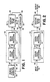
- Figure 1 is a functional block diagram of apparatus in accordance with the present invention. Included in Figure 1 is a Signal Acquisition System 10 ⁇ that has Analog Signal Processing apparatus 12 and Digital Signal Processing apparatus 14.
- Analog Signal Processing apparatus 12 has an input terminal 16 and an output terminal 18 associated therewith, and broadly represents any of a wide variety of analog signal processing circuits, e.g. amplifiers, filters and similar waveform/signal processors.
- Digital Signal Processing apparatus 14 has an input terminal 20 ⁇ and an output terminal 22 associated therewith, and broadly represents any of a wide variety of digital signal processing circuits, e.g., sample/hold apparatus, analog-to-digital converters and digital memory.
- Training Function Generator 30 ⁇ having signal output terminals 32 and 34, and a trigger output terminal 36.
- the output signal produced by Training Function Generator 30 ⁇ appears on terminal 32 in an analog format, and on terminal 34 in a digital format. It is to be understood that in the case where the output signal is binary in nature, i.e., having only two discrete states, the signals produced on terminals 32 and 34 would be identical.
- the trigger signal appearing on terminal 36 occurs coincident with the start of the output signal, and is used for synchronization purposes.
- Adaptive Digital Filter 40 ⁇ having an input terminal 42, a control terminal 44 and an output terminal 46 associated therewith is included, and functions to perform a selected filtering operation on a signal coupled to terminal 42 thereof in accordance with control information coupled to control terminal 44, as more fully discussed hereafter.
- Controller 50 ⁇ having input terminals 52, 54 and 56, and output terminal 58 associated therewith, is included and functions in response to signal information coupled to terminals 52, 54 and 56 thereof to produce control information on terminal 58 thereof for controlling Adaptive Digital Filter 40 ⁇ , as more fully discussed hereafter.
- Training Function Generator 30 ⁇ provides a selected reference signal to Analog Signal Processing apparatus 12 and to Controller 50 ⁇ .
- Analog Signal Processing apparatus 12 and Digital Signal Processing apparatus 14 provide processing on the signal from Training Function Generator 30 ⁇ in accordance with previously selected design criteria. However, as analog systems are subject to frequency limitations, and hence generally do not produce a signal in strict accordance with an intended design criteria.
- the resultant signal from terminal 22 of Digital Signal Processing apparatus 14 therefore departs from an expected signal as a result of the signal processing on the signal produced by Training Function Generator 30 ⁇ .
- Adaptive Digital Filter 40 ⁇ responsive to control information coupled to terminal 44 thereof from Controller 50 ⁇ , functions to provide additional signal processing to remove undesirable effects introduced by Analog Signal Processing apparatus 12 and Digital Signal Processing apparatus 14.
- Controller 50 ⁇ functions to compare the signal from terminal 34 of Training Function Generator 30 ⁇ with the signal from terminal 46 of Adaptive Digital Filter 40 ⁇ , and in response to a detected difference therebetween, to produce control information on terminal 58 thereof which, when coupled to terminal 44 of Adaptive Digital Filter 40 ⁇ , operates to adjust the operation of Adaptive Digital Filter 40 ⁇ so that the resultant signal produced on terminal 46 thereof will closely match the signal from terminal 34 of Training Function Generator 30 ⁇ .
- Adaptive Digital Filter 40 ⁇ functions to process the signal from terminal 22 of Digital Signal Processing apparatus 14 to remove undesirable effects introduced by the combined signal processing of Analog Signal Processing apparatus 12 and Digital Signal Processing apparatus 14.
- Adaptive Digital Filter 40 ⁇ is a Finite Impulse Response Digital Filter having a lattice configuration, with the coefficients associated therewith adjustable in accordance with control information coupled to terminal 44 thereof, as more fully discussed hereafter.
- Controller 50 ⁇ functions to adjust those coefficients to minimize the error between the signal from terminal 34 of Training Function Generator 30 ⁇ and the signal from terminal 46 of Adaptive Digital Filter 40 ⁇ according to a selected correction criteria, as discussed more fully hereafter.
- Training Function Generator 30 ⁇ functions to provide a training signal on terminals 32 and 34 thereof to facilitate a determination of response characteristics of Signal Acquisition System 10 ⁇ .
- the training signal should contain sufficient energy with respect to the frequency band of interest of Signal Acquisition System 10 ⁇ .
- the sampling frequency of Digital Signal Processing apparatus 14 should be high enough to avoid aliasing with respect to the signal produced by Training Function Generator 30 ⁇ .
- Training Function Generator 30 ⁇ further provides on terminal 36 thereof a trigger signal coincident with the generation of the training signal.
- sampling clock in Digital Signal Processing apparatus 14 must be related harmonically in frequency to the frequency of the clock in Training Function Generator 30 ⁇ .
- the training signal produced by Training Function Generator 30 ⁇ may be either a pulse train signal, a random sequence signal, or any signal having characteristics which are previously known by Controller 50 ⁇ . It should be understood with regard to the use of a pulse train signal that significant data with respect to rising or falling edge information of the signal produced thereby may not be detected if the pulses employed have an insufficient duration. In addition, however, if the duration of the pulses employed is too great, the power density spectrum of the high frequency portion will not be adequate to provide sufficient descriptive information with respect to Signal Acquisition System 10 ⁇ . It was consequently empirically determined in a prototype application employing a Model PG 50 ⁇ 2 Pulse Generator manufactured by Tektronix, Inc. of Beaverton, Oregon, that pulses having a duration of at least 20 ⁇ nanoseconds and a frequency of 2.6 MHz represents a good compromise between the requirements in the time and frequency domains.
- FIG. 3 A random sequence generator implementation for Training Function Generator 30 ⁇ ( Figure 1) based upon a seven state Emitter Coupled Logic shift register having a clock rate of 125 MHz is functionally illustrated in Figure 3.
- Figure 3 includes seven cascaded D-Type Flip-Flops 10 ⁇ 0 ⁇ , 110 ⁇ , 120 ⁇ , 130 ⁇ , 140 ⁇ , 150 ⁇ and 160 ⁇ having the Q terminal of the preceding one coupled to the D terminal of following one and the clock terminals are all connected to a common Clock 212.
- the D terminal of Flip-Flop 10 ⁇ 0 ⁇ is coupled to receive the output signal from an Exclusive-NOR Gate 170 ⁇ also inlcuded in Training Function Generator 30 ⁇ .
- Training Function Generator 30 ⁇ further includes a Comparator 180 ⁇ which has seven pairs of input terminals 182 - 20 ⁇ 8 and an output terminal 210 ⁇ .
- Terminal 182 is hardwired to a logic 1 level
- terminals 186, 190 ⁇ 194, 198, 20 ⁇ 2 and 20 ⁇ 6 are each hardwired to a logic 0 ⁇ level
- the other terminals are connected to the Q output terminal of a different one of Flip-Flops 10 ⁇ 0 ⁇ -160 ⁇ .
- Comparator 180 ⁇ functions responsive to the simultaneous occurrence of identical logic states on each pair of input terminals to produce a corresponding signal on output terminal 210 ⁇ , as discussed more fully hereafter.
- Comparator 180 ⁇ was implemented by a Model F10 ⁇ 0 ⁇ 166 integrated circuit manufactured by Fairchild Instruments of Mountain View, California.
- the final element of Training Function Generator 30 ⁇ is Level Shifter 210 ⁇ .
- Level Shifter 210 ⁇ is included to shift the voltage level of the binary signal from the Q terminal of Flip-Flop 160 ⁇ to a selected voltage level as the output signal of Training Function Generator 30 ⁇ .
- the selected voltage levels which are associated with Level Shifter 210 ⁇ are selected for the particular application in which the apparatus of Figure 3 is used.
- Clock 212 is selected to have a frequency of 125 MHz. It will be understood that as the output signal produced by the apparatus of Figure 3 is binary in nature, the signal produced by Level Shifter 210 ⁇ would correspond to both terminal 32 and 34 of Figure 1.
- D-Type Flip-Flops 10 ⁇ 0 ⁇ , 110 ⁇ , 120 ⁇ , 130 ⁇ , 140 ⁇ , 150 ⁇ and 160 ⁇ collectively operate as a seven stage shift register, in response to a signal from Clock 212, to shift an output signal of Exclusive-NOR Gate 170 ⁇ therethrough.
- the output signal of Exclusive-NOR Gate 170 ⁇ is produced by a logical exclusive-NOR operation on the output signals from Q-Output terminals of D-Type Flip-Flops 10 ⁇ 0 ⁇ and 160 ⁇ , respectively.
- the output signal from Q-Output terminal of D-Type Flip-Flop 160 ⁇ froms the output signal for the random sequence generator of Figure 3, and is consequently coupled to Level Shifter 210 ⁇ .
- Comparator 180 ⁇ continuously monitors the states of the D-Type Flip-Flops which comprise the seven stage shift register, and produces a trigger signal when the logic state of D-Type Flip-Flop 10 ⁇ 0 ⁇ is a logic one, and the logic states of the remaining D-Type Flip-Flops 110 ⁇ -160 ⁇ are a logic zero.
- the power density spectrum of the apparatus of Figure 3 has been demonstrated to have a range from DC to at least 70 ⁇ MHz, with a magnitude decay of less than 6dB. Compensation having increased frequency content may be achieved for broader band distorted systems by increasing the clock frequency.
- FIG 4 is a functional block diagram of an implementation for Adaptive Digital Filter 40 ⁇ of Figures 1 and 2.
- Digital Delay 220 ⁇ functions to delay a digital word coupled thereto from terminal 42 of Adaptive Digital Filter 40 ⁇ by one clock period.
- Digital Delays 230 ⁇ and 240 ⁇ operate in an identical fashion with respect to digital words coupled thereto from Digital Adders 228 and 238, respectively.
- Coefficient Multipliers 222 and 224 operate to produce an output digital word equal to the product of a constant a1 and a digital word coupled thereto from terminal 42 of Adaptive Digital Filter 40 ⁇ and from Digital Delay 220 ⁇ , respectively.
- the constant a1 is coupled to Coefficient Multipliers 222 and 224 from terminal 58 of Controller 50 ⁇ ( Figure 5), as more fully discussed hereafter.
- Coefficient Mulitpliers 232 and 234 operate in a similar fashion to produce an output digital word equal to the product of a constant a2 and a digital word coupled thereto from Digital Adder 226 and Digital Delay 230 ⁇ , respectively.
- the constant a2 is coupled to Coefficient Multipliers 232 and 234 from terminal 58 of Controller 50 ⁇ ( Figure 5), as more fully discussed hereafter.
- Coefficient Multipliers 242 and 244 operate in a similar fashion to produce an output digital word equal to the product of a constant a3 and a digital word coupled from Digital Adder 236 and Digital Delay 240 ⁇ , respectively.
- the constant a3 is coupled to Coefficient Multipliers 242 and 244 from terminal 58 of Controller 50 ⁇ ( Figure 5), as more fully discussed hereafter.
- Digital Adder 226 operates to produce a digital word equal to a difference between the digital words coupled thereto from terminal 42 of Adaptive Digital Filter 40 ⁇ and Coefficient Multiplier 224.
- Digital Adder 228 operates to produce a digital word equal to a difference between the digital words coupled thereto from Digital Delay 220 ⁇ and Coefficient Multiplier a1 222.
- Digital Adders 236, 238, 246 and 248 operate in a similar manner.
- Coefficient Multiplier 250 ⁇ operates to produce an output digital word equal to a product of a constant b1 and a digital word coupled thereto from Digital Delay 220 ⁇ .
- the contant b1 is coupled to Coefficient Multiplier 250 ⁇ from terminal 58 of Controller 50 ⁇ ( Figure 5), as more fully discussed hereafter.
- Coefficient Multiplier 252 operates to produce a digital word equal to a product of a constant b2 and a digital word coupled thereto from Digital Delay 230 ⁇ .
- the constant b2 is coupled to Coefficient Multiplier 252 from terminal 58 of Controller 50 ⁇ ( Figure 5), as more fully discussed hereafter.
- Coefficient Multiplier 252 operates to produce a digital word equal to the product of a constant b3 and a digital word coupled thereto from Digital Delay 240 ⁇ .
- Adaptive Digital Filter 40 ⁇ is comprised of a plurality of sections: Digital Delay 220 ⁇ , Coefficient Multipliers 222 and 224, Digital Adders 226 and 228, and Coefficient Multiplier 250 ⁇ collectively comprise a first section of Adaptive Digital Filter 40 ⁇ ; Digital Delay 230 ⁇ , Coefficient Multipliers 232 and 234, Digital Adders 236 and 238, and Coefficient Multiplier 252 collectively comprise a second section; and Digital Delay 240 ⁇ , Coefficient Multipliers 242 and 244, Digital Adders 246 and 248, and Coefficient Multiplier 254 comprise a third section.
- Adaptive Digital Filter 40 ⁇ An output signal from each of such sections is taken following the digital delay associated with the section, as more fully discussed hereafter. It is to be understood that the number of sections which are included in Adaptive Digital Filter 40 ⁇ would be determined by considerations associated with the particular application in which the adaptive digital filter would be used, as would be apparent to one of ordinary skill in the art.
- Digital Summer 256 operates to produce a digital signal on terminal 46 of Adaptive Digital Filter 40 ⁇ equal to the sum of the digital signals from each of the sections of Adaptive Digital Filter 40 ⁇ , e.g., for the functional implementation of Adaptive Digital Filter 40 ⁇ illustrated in Figure 4 having a total of three sections, the signal produced on terminal 46 thereof would be equal to the sum of the signals from Coefficient Multipliers 250 ⁇ , 252 and 254.
- FIG. 5 is a functional block diagram of an implementation for Controller 50 ⁇ of Figures 1 and 2.
- Digital Adder 260 ⁇ operates to produce a digital word equal to a difference between the digital word coupled to terminal 52 of Controller 50 ⁇ , i.e., the digital word from terminal 34 of Training Function Generator 30 ⁇ ( Figure 1), and the digital word coupled to terminal 56 of Controller 50 ⁇ , i.e., the digital word from Digital Summer 256 ( Figure 4).
- the results of the operation performed by Digital Adder 260 ⁇ is coupled to Microprocessor 262.
- Microprocessor 262 responsive to the information from Digital Adder 260 ⁇ , operates to determine the coefficients associated with Adaptive Digital Filter 40 ⁇ , i.e., the coefficients which are to be coupled to Coefficient Multipliers 222, 224, 232, 234, 242, 244, 250 ⁇ , 252 and 254 ( Figure 4), as more fully discussed hereafter.
- the trigger signal from terminal 36 of Training Function Generator 30 ⁇ ( Figure 1) operates to indicate to Microprocessor 262 the point in time to start acquiring data when the foregoing described apparatus is being used as a digital compensator ( Figures 1 and 2).
- Microprocessor 262 has associated therewith Program RAM/ROM 264 which stores the program which Microprocessor 262 executes to determine the foregoing described coefficients, and data RAM 266 which provides temporary storage of computations made in the execution of the program.
- FIG. 6 is a flow chart of the program which Microprocessor 262 executes to determine the foregoing described coefficients.
- y(n) in block 270 ⁇ corresponds to a collection of data points associated with the signal from terminal 34 of Training Function Generator 30 ⁇ ( Figure 1).
- Microprocessor 260 ⁇ operates to collect and store in e(n) a set of data points, e.g., y(1) would be a first data point, y(2) a second data point, and in general y(n) would correspond to the nth data point.
- the number of data points which are collected is determined by the nature of a particular application, as would be apparent to one of ordinary skill in the art.
- a collection of data points associated with the signal from terminal 46 of Adaptive Digital Filter 40 ⁇ ( Figure 4) are likewise collected, and assigned to a variable "z".
- data associated with the (n-1)th data point is assigned to the value of z(n).
- An index counter "i" is initialized to a starting value of zero in block 274. The index counter is used to control the number of times the sequence of steps in blocks 278, 280,282,284 and 286 are performed.
- the value of the index counter is compared against a maximum value, "M", to determine if the foregoing referenced sequence of steps have been performed the required number of times.
- the maximum value "M” corresponds to the number of sections present in Adaptive Digital Filter 40 ⁇ , e.g., for Adaptive Digital Filter 40 ⁇ illustrated in Figure 4, "M” would have a value of 3.
- the index counter is next incremented in block 278 to a value of one. Thereafter the value for the coefficient a1 is next computed in block 280 ⁇ . It will be understood that the coefficient a1 corresponds to the constant a1 previously discussed with respect to Coefficient Multipliers 222 and 224 ( Figure 4).
- the value for the coefficient b1 is next determined in block 282. It will be understood in this regard that the coefficient b1 corresponds to the constant b1 previously discussed with respect to Coefficient Multiplier 250 ⁇ ( Figure 4). Thereafter, a new set of values for e(n), z(n) and x(n) for use in determining values for subsequent coefficients are next determined in blocks 284 and 286. Thereafter, the value of the index counter is again compared against the previously discussed maximum value in block 276, and the foregoing described series of steps in blocks 278,280,282,284 and 286 are again performed for the next value of the index counter.
- Training Function Generator 30 ⁇ and Controller 50 ⁇ may be removed, and Signal Acquisition System 10 ⁇ and Adaptive Digital Filter 40 ⁇ used for the processing of Input Signal 70 ⁇ ( Figure 2).
- Training Function Generator 30 ⁇ may alternately operate to produce an output signal on terminals 32 and 34 responsive to receipt of a trigger signal on terminal 36 from Controller 50 ⁇ .
- Microprocessor 262 would produce the trigger signal on terminal 54 of Controller 50 ⁇ ( Figure 5), and thereafter perform the previously discussed sequence of steps beginning with block 270 ⁇ ( Figure 6).
- the digital compensator/equalizer may be used to equalize two or more signal channels.
- one signal channel is used as a reference channel, and the remaining signal channels are equalized such that a common input to all of the channels will produce output signals similar to that in the reference channel.
- Figure 7 is a functional block diagram of apparatus in accordance with the method and apparatus of the present invention with respect to the equalization of two or more channels.
- Signal Acquisition Systems 30 ⁇ 0 ⁇ and 320 ⁇ each represent an independent signal channel, and are each identical to Signal Acquisition System 10 ⁇ previously discussed with respect to Figures 1 and 2.
- Signal Acquisition System 30 ⁇ 0 ⁇ includes Analog Signal Processing apparatus 30 ⁇ 2 and Digital Signal Processing apparatus 30 ⁇ 4, and
- Signal Acquisition System 320 ⁇ includes Analog Signal Processing apparatus 322 and Digital Signal Processing apparatus 324.
- Waveform Generator 340 ⁇ Also included in the functional block diagram of Figure 7 is Waveform Generator 340 ⁇ .
- Adaptive Digital Filter 40 ⁇ and Controller 50 ⁇ are identical to Adaptive Digital Filter 40 ⁇ and Controller 50 ⁇ previously discussed with respect to Figure 1.
- the apparatus of Figure 7 is configured as is the apparatus in Figure 1 with Signal Acquisition System 30 ⁇ 0 ⁇ in place of Signal Acquisition System 10 ⁇ and Signal Acquisition System 320 ⁇ inserted in the signal path between the signal source, Waveform Generator 340 ⁇ , and Controller 50 ⁇ .
- Waveform Generator 340 ⁇ functions to provide a signal on terminal 342 thereof to facilitate a determination of response characteristics of Signal Acquisition Systems 30 ⁇ 0 ⁇ and 320 ⁇ .
- the signal should contain sufficient energy with respect to the frequency band of interest of Signal Acquisition Systems 30 ⁇ 0 ⁇ and 320 ⁇ .
- the sampling frequency of Digital Signal Processing apparatus 30 ⁇ 4 and 324 should be high enough to avoid aliasing with respect to the signal produced by Waveform Generator 340 ⁇ .
- Waveform Generator 340 ⁇ was selected to generate a clipped FM signal that sweept a wide frequency range that could be approximated by a one-zero sequence.
- Waveform Generator 340 ⁇ provides a selected reference signal to Analog Signal Processing apparatus 30 ⁇ 2 and 322. It will be understood in this regard that as an identical signal is being coupled to both Signal Acquisition System 30 ⁇ 0 ⁇ and 320 ⁇ , the trigger signal previously discussed with respect to Figure 1, i.e., the signal coupled between terminal 36 of Training Function Generator 30 ⁇ and terminal 54 of Controller 50 ⁇ , is not required.
- Analog Signal Processing apparatus 30 ⁇ 2 and Digital Signal Processing apparatus 30 ⁇ 4 provide processing on the signal from Waveform Generator 340 ⁇ in accordance with previously selected design criteria.
- Analog Signal Processing apparatus 322 and Digital Signal Processing apparatus 324 likewise provide processing on the signal from Wavefrom Generator 340 ⁇ in accordance with previously selected design criteria.
- Adaptive Digital Filter 40 ⁇ responsive to control information coupled to terminal 44 thereof from Controller 50 ⁇ functions to provide additional signal processing functions to minimize differences between the signal from Signal Acquisition System 30 ⁇ 0 ⁇ and the corresponding signal from Signal Acquisition System 320 ⁇ .
- Controller 50 ⁇ functions to compare the signal from Digital Signal Processing apparatus 324 with the signal from Adaptive Digital Filter 40 ⁇ , and in response to a detected difference therebetween, to produce control information on terminal 58 thereof which, when coupled to terminal 44 of Adaptive Digital Filter 40 ⁇ , operates to adjust the operation of Adaptive Digital Filter 40 ⁇ so that the resultant signal produced on terminal 46 thereof will closely match the signal from Digital Signal Processing apparatus 324.
- Adaptive Digital Filter 40 ⁇ and Controller 50 ⁇ illustrated in Figure 7 operate in an identical manner as was previously discussed with respect to Figures 4, 5 and 6. It is to be understood that any of a variety of correction criteria may be employed by Controller 50 ⁇ in the digital equalization application discussed with respect to Figure 7, as would be apparent to one of ordinary skill in the art. Consequently, the method and apparatus of the present invention is not to be considered as being restricted to employing a Least Mean Square correction criteria for digital equalization applications.
Landscapes
- Filters That Use Time-Delay Elements (AREA)
- Cable Transmission Systems, Equalization Of Radio And Reduction Of Echo (AREA)
Applications Claiming Priority (2)
| Application Number | Priority Date | Filing Date | Title |
|---|---|---|---|
| US947158 | 1986-12-29 | ||
| US06/947,158 US4789952A (en) | 1986-12-29 | 1986-12-29 | Method and apparatus for digital compensation and digital equalization |
Publications (2)
| Publication Number | Publication Date |
|---|---|
| EP0273581A2 true EP0273581A2 (fr) | 1988-07-06 |
| EP0273581A3 EP0273581A3 (fr) | 1989-12-13 |
Family
ID=25485628
Family Applications (1)
| Application Number | Title | Priority Date | Filing Date |
|---|---|---|---|
| EP87310351A Withdrawn EP0273581A3 (fr) | 1986-12-29 | 1987-11-24 | Méthode et appareil de compensation numérique et d'égalisation numérique |
Country Status (3)
| Country | Link |
|---|---|
| US (1) | US4789952A (fr) |
| EP (1) | EP0273581A3 (fr) |
| JP (1) | JPS63174419A (fr) |
Cited By (6)
| Publication number | Priority date | Publication date | Assignee | Title |
|---|---|---|---|---|
| NL8902618A (nl) * | 1988-10-21 | 1990-05-16 | Mitsubishi Electric Corp | Toonbesturingsinrichting. |
| DE3916256A1 (de) * | 1989-05-18 | 1990-11-22 | Ant Nachrichtentech | Digitalfilter mit daempfungs- und phasengangentzerrung |
| DE3916236A1 (de) * | 1989-05-18 | 1990-11-22 | Ant Nachrichtentech | Digitalfilter mit daempfungs- und phasengangentzerrung |
| EP0453293A2 (fr) * | 1990-04-19 | 1991-10-23 | Matsushita Electric Industrial Co., Ltd. | Appareil adaptatif au champ sonore |
| EP0504988A2 (fr) * | 1991-03-21 | 1992-09-23 | Philips Patentverwaltung GmbH | Circuit de réglage de la réponse en fréquence d'un signal audio numérique |
| EP2392075A2 (fr) * | 2009-01-27 | 2011-12-07 | ADC Telecommunications, Inc. | Procédé et appareil destinés à égaliser de manière numérique un signal dans un système d'antenne réparti |
Families Citing this family (9)
| Publication number | Priority date | Publication date | Assignee | Title |
|---|---|---|---|---|
| EP0413073A1 (fr) * | 1989-08-16 | 1991-02-20 | International Business Machines Corporation | Filtre de phase à gain de boucle adaptatif |
| US5222101A (en) * | 1991-05-03 | 1993-06-22 | Bell Communications Research | Phase equalizer for TDMA portable radio systems |
| US5432818A (en) * | 1993-02-16 | 1995-07-11 | Lou; Yuang | Method and apparatus of joint adaptive channel encoding, adaptive system filtering, and maximum likelihood sequence estimation process by means of an unknown data training |
| US5576976A (en) * | 1993-09-07 | 1996-11-19 | Rockwell International Corporation | Amplitude detection and automatic gain control of a sparsely sampled sinusoid by adjustment of a notch filter |
| US5940441A (en) * | 1996-10-29 | 1999-08-17 | International Business Machines Corporation | Integrated adaptive cable equalizer using a continuous-time filter |
| US6490535B1 (en) * | 1999-04-15 | 2002-12-03 | Tektronix, Inc. | Method and apparatus for calibrating an instrument |
| US6725169B2 (en) | 2002-03-07 | 2004-04-20 | Honeywell International Inc. | Methods and apparatus for automatic gain control |
| US20040218701A1 (en) * | 2003-04-29 | 2004-11-04 | Prashant Singh | Protocol agnostic method for adaptive equalization |
| US8687744B2 (en) * | 2006-01-18 | 2014-04-01 | Broadcom Corporation | Method and system for an improved cellular diversity receiver |
Citations (3)
| Publication number | Priority date | Publication date | Assignee | Title |
|---|---|---|---|---|
| US3390336A (en) * | 1966-01-24 | 1968-06-25 | Cardion Electronics Inc | Apparatus and method for converting an input wave signal using adaptive network adjusted to time inverse of translating channel |
| US3629736A (en) * | 1970-10-02 | 1971-12-21 | Bell Telephone Labor Inc | System for generating initial settings for an automatic transversal equalizer |
| FR2159332A1 (fr) * | 1971-11-08 | 1973-06-22 | Gretag Ag |
Family Cites Families (9)
| Publication number | Priority date | Publication date | Assignee | Title |
|---|---|---|---|---|
| JPS51132066A (en) * | 1975-05-13 | 1976-11-16 | Mitsubishi Electric Corp | A-d converter |
| US4141072A (en) * | 1976-12-28 | 1979-02-20 | Xerox Corporation | Frequency domain automatic equalizer using minimum mean square error correction criteria |
| US4539689A (en) * | 1978-04-26 | 1985-09-03 | Racal Data Communications, Inc. | Fast learn digital adaptive equalizer |
| JPS5753145A (en) * | 1980-09-16 | 1982-03-30 | Sony Tektronix Corp | Calibrator for analogue-digital converter |
| US4397029A (en) * | 1981-02-17 | 1983-08-02 | The United States Of America As Represented By The Secretary Of The Navy | Least squares adaptive lattice equalizer |
| IT1159389B (it) * | 1983-04-19 | 1987-02-25 | Cselt Centro Studi Lab Telecom | Equalizzatore adattativo per segnali numerici |
| US4637035A (en) * | 1984-02-16 | 1987-01-13 | Paradyne Corporation | Digital modem for multiple telephone circuits |
| US4581747A (en) * | 1984-03-05 | 1986-04-08 | At&T Bell Laboratories | Arrangement for equalizing the variable attenuation of a signal on a communication line |
| US4695969A (en) * | 1984-12-17 | 1987-09-22 | American Telephone And Telegraph Company At&T Bell Laboratories | Equalizer with improved performance |
-
1986
- 1986-12-29 US US06/947,158 patent/US4789952A/en not_active Expired - Lifetime
-
1987
- 1987-11-24 EP EP87310351A patent/EP0273581A3/fr not_active Withdrawn
- 1987-12-28 JP JP62336745A patent/JPS63174419A/ja active Pending
Patent Citations (3)
| Publication number | Priority date | Publication date | Assignee | Title |
|---|---|---|---|---|
| US3390336A (en) * | 1966-01-24 | 1968-06-25 | Cardion Electronics Inc | Apparatus and method for converting an input wave signal using adaptive network adjusted to time inverse of translating channel |
| US3629736A (en) * | 1970-10-02 | 1971-12-21 | Bell Telephone Labor Inc | System for generating initial settings for an automatic transversal equalizer |
| FR2159332A1 (fr) * | 1971-11-08 | 1973-06-22 | Gretag Ag |
Non-Patent Citations (1)
| Title |
|---|
| IEE PROCEEDINGS, SECTION A-I, vol. 131, no. 5, part F, August 1984, pages 473-479, Old Woking, Surrey, GB; P.M. GRANT et al.: "Application of gradient adaptive lattice filters to channel equalisation" * |
Cited By (10)
| Publication number | Priority date | Publication date | Assignee | Title |
|---|---|---|---|---|
| NL8902618A (nl) * | 1988-10-21 | 1990-05-16 | Mitsubishi Electric Corp | Toonbesturingsinrichting. |
| DE3916256A1 (de) * | 1989-05-18 | 1990-11-22 | Ant Nachrichtentech | Digitalfilter mit daempfungs- und phasengangentzerrung |
| DE3916236A1 (de) * | 1989-05-18 | 1990-11-22 | Ant Nachrichtentech | Digitalfilter mit daempfungs- und phasengangentzerrung |
| EP0453293A2 (fr) * | 1990-04-19 | 1991-10-23 | Matsushita Electric Industrial Co., Ltd. | Appareil adaptatif au champ sonore |
| EP0453293A3 (en) * | 1990-04-19 | 1992-12-02 | Matsushita Electric Industrial Co., Ltd. | Sound field variable apparatus |
| EP0504988A2 (fr) * | 1991-03-21 | 1992-09-23 | Philips Patentverwaltung GmbH | Circuit de réglage de la réponse en fréquence d'un signal audio numérique |
| EP0504988A3 (en) * | 1991-03-21 | 1993-06-09 | Philips Patentverwaltung Gmbh | Circuit arrangement to control the frequency response of a digital audio signal |
| EP2392075A2 (fr) * | 2009-01-27 | 2011-12-07 | ADC Telecommunications, Inc. | Procédé et appareil destinés à égaliser de manière numérique un signal dans un système d'antenne réparti |
| CN102301606A (zh) * | 2009-01-27 | 2011-12-28 | Adc长途电讯有限公司 | 对分布式天线系统中的信号进行数字均衡的方法和装置 |
| EP2392075A4 (fr) * | 2009-01-27 | 2013-08-07 | Adc Telecommunications Inc | Procédé et appareil destinés à égaliser de manière numérique un signal dans un système d'antenne réparti |
Also Published As
| Publication number | Publication date |
|---|---|
| JPS63174419A (ja) | 1988-07-18 |
| EP0273581A3 (fr) | 1989-12-13 |
| US4789952A (en) | 1988-12-06 |
Similar Documents
| Publication | Publication Date | Title |
|---|---|---|
| EP0273581A2 (fr) | Méthode et appareil de compensation numérique et d'égalisation numérique | |
| EP0610683B1 (fr) | Circuit numérique de récuperation d'horloge | |
| EP0544647B1 (fr) | Calcul des facteurs de filtrage pour filtre numérique | |
| DE69012164T2 (de) | Digitaler Fir-Filter für Hochgeschwindigkeits-Kommunikationssysteme. | |
| JPH09200042A (ja) | 複合位相濾波器とこれを用いたタイミング誤差補償装置及びその方法 | |
| US4323864A (en) | Binary transversal filter | |
| Darlington | A history of network synthesis and filter theory for circuits composed of resistors, inductors, and capacitors | |
| US5805479A (en) | Apparatus and method for filtering digital signals | |
| DE69232966T2 (de) | Taktwiedergewinnungsverfahren und -system | |
| Spaulding | Synthesis of Pulse‐Shaping Networks in the Time Domain | |
| EP0374214B1 (fr) | Filtre apparie rectangulaire a rapport variable | |
| DE102011116217A1 (de) | Verwendung eines multilevel-pulsweitenmodulierten Signals zur Realzeit-Rauschauslöschung | |
| US4755961A (en) | Digital tank circuit | |
| US4794556A (en) | Method and apparatus for sampling in-phase and quadrature components | |
| US3931604A (en) | Sampling automatic equalizer | |
| Vallancourt et al. | A fully programmable sampled-data analog CMOS filter with transfer-function coefficients determined by timing | |
| JPS63211824A (ja) | 波形等化器 | |
| CA1145051A (fr) | Convertisseur de spectre pour signaux analogiques | |
| CA1116703A (fr) | Filtres digitaux a controle des cycles de limite | |
| JPH05327409A (ja) | レート変換方法及びその変換回路 | |
| US4535295A (en) | Method and device for controlling the phase of timing signal | |
| AU601489B2 (en) | A sampled data tone control system | |
| US5657353A (en) | Pulse shaping filter for received digital transmissions using phase lock loop for adjusting shift register | |
| EP0653121B1 (fr) | Synchroniseur audio numerique | |
| JP3146609B2 (ja) | 自動等化回路 |
Legal Events
| Date | Code | Title | Description |
|---|---|---|---|
| PUAI | Public reference made under article 153(3) epc to a published international application that has entered the european phase |
Free format text: ORIGINAL CODE: 0009012 |
|
| AK | Designated contracting states |
Kind code of ref document: A2 Designated state(s): DE FR GB NL |
|
| PUAL | Search report despatched |
Free format text: ORIGINAL CODE: 0009013 |
|
| AK | Designated contracting states |
Kind code of ref document: A3 Designated state(s): DE FR GB NL |
|
| 17P | Request for examination filed |
Effective date: 19900320 |
|
| STAA | Information on the status of an ep patent application or granted ep patent |
Free format text: STATUS: THE APPLICATION IS DEEMED TO BE WITHDRAWN |
|
| 18D | Application deemed to be withdrawn |
Effective date: 19910603 |
|
| RIN1 | Information on inventor provided before grant (corrected) |
Inventor name: THONG, TRAN Inventor name: LO, PEI-HWA |