EP0268401A2 - Systèmes de mémoire à semi-conducteur et méthodes pour les faire fonctionner - Google Patents
Systèmes de mémoire à semi-conducteur et méthodes pour les faire fonctionner Download PDFInfo
- Publication number
- EP0268401A2 EP0268401A2 EP87309700A EP87309700A EP0268401A2 EP 0268401 A2 EP0268401 A2 EP 0268401A2 EP 87309700 A EP87309700 A EP 87309700A EP 87309700 A EP87309700 A EP 87309700A EP 0268401 A2 EP0268401 A2 EP 0268401A2
- Authority
- EP
- European Patent Office
- Prior art keywords
- memory
- memory cells
- address
- cells
- defective
- Prior art date
- Legal status (The legal status is an assumption and is not a legal conclusion. Google has not performed a legal analysis and makes no representation as to the accuracy of the status listed.)
- Withdrawn
Links
Images


Classifications
-
- G—PHYSICS
- G11—INFORMATION STORAGE
- G11C—STATIC STORES
- G11C29/00—Checking stores for correct operation ; Subsequent repair; Testing stores during standby or offline operation
-
- G—PHYSICS
- G11—INFORMATION STORAGE
- G11C—STATIC STORES
- G11C29/00—Checking stores for correct operation ; Subsequent repair; Testing stores during standby or offline operation
- G11C29/70—Masking faults in memories by using spares or by reconfiguring
-
- G—PHYSICS
- G11—INFORMATION STORAGE
- G11C—STATIC STORES
- G11C29/00—Checking stores for correct operation ; Subsequent repair; Testing stores during standby or offline operation
- G11C29/04—Detection or location of defective memory elements, e.g. cell constructio details, timing of test signals
- G11C29/08—Functional testing, e.g. testing during refresh, power-on self testing [POST] or distributed testing
- G11C29/12—Built-in arrangements for testing, e.g. built-in self testing [BIST] or interconnection details
- G11C29/38—Response verification devices
- G11C29/42—Response verification devices using error correcting codes [ECC] or parity check
-
- G—PHYSICS
- G11—INFORMATION STORAGE
- G11C—STATIC STORES
- G11C29/00—Checking stores for correct operation ; Subsequent repair; Testing stores during standby or offline operation
- G11C29/04—Detection or location of defective memory elements, e.g. cell constructio details, timing of test signals
- G11C29/08—Functional testing, e.g. testing during refresh, power-on self testing [POST] or distributed testing
- G11C29/12—Built-in arrangements for testing, e.g. built-in self testing [BIST] or interconnection details
- G11C29/44—Indication or identification of errors, e.g. for repair
-
- G—PHYSICS
- G06—COMPUTING OR CALCULATING; COUNTING
- G06F—ELECTRIC DIGITAL DATA PROCESSING
- G06F11/00—Error detection; Error correction; Monitoring
- G06F11/07—Responding to the occurrence of a fault, e.g. fault tolerance
- G06F11/0703—Error or fault processing not based on redundancy, i.e. by taking additional measures to deal with the error or fault not making use of redundancy in operation, in hardware, or in data representation
- G06F11/0751—Error or fault detection not based on redundancy
- G06F11/0754—Error or fault detection not based on redundancy by exceeding limits
- G06F11/076—Error or fault detection not based on redundancy by exceeding limits by exceeding a count or rate limit, e.g. word- or bit count limit
-
- G—PHYSICS
- G06—COMPUTING OR CALCULATING; COUNTING
- G06F—ELECTRIC DIGITAL DATA PROCESSING
- G06F11/00—Error detection; Error correction; Monitoring
- G06F11/07—Responding to the occurrence of a fault, e.g. fault tolerance
- G06F11/08—Error detection or correction by redundancy in data representation, e.g. by using checking codes
- G06F11/10—Adding special bits or symbols to the coded information, e.g. parity check, casting out 9's or 11's
- G06F11/1008—Adding special bits or symbols to the coded information, e.g. parity check, casting out 9's or 11's in individual solid state devices
Definitions
- the invention relates to computer semiconductor memories. More particularly, the invention relates to self-testing and self-repairing computer memory systems and a method for making and using them.
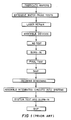
- Figure 1 shows a prior-art method for testing and constructing dynamic RAM memories. After fabricating the wafers and before cutting them into individual chips the prior art conducts comprehensive wafer probe tests on the entire wafer.
- One such test is a D.C. fail test. This test measures the power supply current drawn by each die in active mode and standby mode. If a die draws too much current in either mode, the tester discards the die because the tester assumes the die has a short.
- Other wafer probe tests conducted on the individual cells, address decoders, and sense amplifiers determine their functionality.
- a laser repair procedure replaces defective memory cells with redundant rows and columns. If the number or placement of redundant rows and columns is not sufficient to repair the defective memory cells, the die is discarded. After completion of laser repair, the prior art retests the wafer. All failing die must be discarded because the prior-art procedures have no way to repair them.
- the wafer After completing tests on the wafer, the wafer is diced into separate chips and assembled into separate packages. These packaged chips are tested for defects and then endure burn-in tests lasting approximately two days at elevated temperatures of 125°C. After passing the burn-in test, the devices encounter the manufacturer's final tests. These time-consuming, expensive tests include a pattern disturb test and write recovery test in addition to other tests.
- the chip manufacturer ships passing devices to customers who typically conduct the incoming screening tests on a sample of the devices. After installing these devices into memory systems, the customer tests the memory systems. These tests typically include a second burn-in test.
- Prior-art procedures use expensive equipment.
- the prior art handles the chips extensively and exposes them to electrostatic discharge and other hostile conditions that cause failures.
- prior-art procedures inefficiently test for pattern sensitive defects.
- Pattern sensitive defects are memory defects that cause failures when the bits have a particular configuration.
- the prior art conducts tests for these pattern sensitive defects by storing every possible combination of ones and zeros into the memory. Obviously, this procedure is very time consuming if not impossible. Therefore, prior-art procedures miss some pattern sensitive defects. These undetected defects will cause system failures when they occur during field use.
- a method of operating a semiconductor memory system comprising the steps of performing, writing and reading operations to and from cells of the system in accordance with stored predetermined addresses which define the cells allocated to particular addresses; detecting any error in data read and determining the address from which it derived; and substituting for the cells pre-allocated to that address other cells of the memory system not otherwise allocated.
- the invention proposes a semiconductor memory system comprising a plurality of memory cells, a system controller, an error detector and an address interpreter, wherein the error detector can detect errors in data retrieved from the memory cells, and the controller can cause substitution of a first memory address by a second in response to detection of a fault associated with the first address, so that thereafter the address interpreter employs the second address and the memory cells of the first address remain unused.
- the self-testing and self-repairing memory system contains memory cells that have passed an abbreviated wafer probe test, a system controller that coordinates testing and repairing, a rewritable table for storing the location of substitute memory cells, an address interpreter for obtaining the correct address and an error correction code engine (ECC engine) that corrects as well as detects errors.
- ECC engine error correction code engine
- a method for making a self-testing and self-repairing memory system exploits the self-testing and self-repairing capability of the memory system.
- the method assemblies all the parts listed above.
- the system controller conducts an initial self-test on the memory chips to determine the size and location of defects.
- the system controller determines whether to replace the defects or have the ECC engine correct the defects. Large groups of defective memory cells are typically replaced to avoid overburdening the error correction code engine.
- the system controller replaces defective memory cells by storing the addresses of the substitute memory cells and the defective memory cells into the rewritable table.
- the present invention for the method of using the self-testing and self-repairing memory system detects, corrects, and repairs defective memory cells during normal operation.
- the system controller tests the memory system and replaces the larger groups of defects.
- the error correction code engine begins its constant search for errors.
- the ECC engine corrects newly located defects, soft errors, and defects that the system controller decided not to replace. Meanwhile, the system controller monitors the number of defects and replaces the larger groups of defects.
- Memory systems have several advantages which result in lower manufacturing cost and greater memory system reliability.
- memory systems require fewer tests during their manufacture.
- a memory system according to the present invention can repair defects at any time. Therefore, these memory systems delay most testing until the last step in the manufacturing process.
- Prior-art memory systems are repaired before the chips are passivated. Since this occurs early in the manufacturing process, the prior art must conduct two sets of tests. One set of tests searches for memory defects to repair before the chip is passivated. An additional set of tests must be conducted at the end of the manufacturing process to locate defects that have arisen since the first set of tests.
- memory systems correct pattern sensitive errors during field use of the memory system
- Prior-art memory systems can not correct the pattern sensitive defects during field use. Therefore, the prior-art memory systems must conduct extensive tests to locate these elusive defects. Tests for pattern sensitive defects are expensive and increase the cost of memory systems.
- memory systems can detect and repair its own defects at any time. This advantage permits memory systems to use memory devices that have a few defects. In contrast, if a prior-art memory system has any defects after the laser repair step, that memory system must be discarded. This decreases the yields of prior art memory systems. Furthermore, if a prior-art memory system obtains a defect during field use, this defect will cause a system failure.
- memory systems have increased reliability. Unlike the prior-art memory systems, they can recover from both hard and soft errors that occur during normal operation. In addition, it can detect the occurrence of new defects and determine the rate at which they occur. Based on this information, the memory system controller estimates future reliability of the memory system and reports this information to the host computer. If necessary, the system controller can request a service call.
- FIG. 3 shows the preferred embodiment of the self-testing and self-repairing memory system.
- This memory system 3-15 contains memory chips 3-1 having numerous memory cells 3-5 that have passed an abbreviated wafer probe test, a system controller 3-13 with firmware that executes self-testing and self-repairing algorithms, a non-volatile table, a substitute address table 3-11 that is rewritable, an address interpreter 3-9, and an error correction code engine 3-3 that detects and corrects errors in the stored data.
- the abbreviated wafer probe test detects chips requiring excessive operating current, requiring excessive standby current, or having an excessive number of nonfunctioning memory cells 3-5. These symptoms often result from defects in the power supply lines, address lines, and other gross failures. The manufacturer discards chips with gross defects and assembles the remaining chips into memory systems.
- the acceptable chips 3-1 are assembled into clusters.
- Each cluster of the memory chips 3-1 has a substitute address table 3-11.
- Each channel 3-7 has an address interpreter 3-9.
- Each memory system 3-15 contains a system controller 3-13 and an error correction code engine 3-3.
- the preferred embodiment of the memory system 3-15 contains an address interpreter 3-9.
- the address interpreter 3-9 produces the address of substitute memory cell 3-5 when presented with the address of a replaced memory cell 3-5. Whenever the host computer system accesses a memory location, it sends the address to the address interpreter 3-9.
- the address interpreter 3-9 queries the substitute address table 3-11 to determine if that memory cell 3-5 has been replaced and to determine the address of that memory cell 3-5.
- the substitute address table 3-11 can have several different embodiments. It can be a look-up table which contains an entry for each memory location. Each address presented to a look-up table 3-11 addresses an unique entry in the look-up table 3-11. If the corresponding memory location has been replaced, the look-up table entry contains the address of the substitute memory cell 3-5.
- the substitute address table 3-11 can have the form of a content addressable memory.
- the memory address presented is compared with the entries in the content addressable memory 3-11. If the desired address does not match an entry of the content addressable memory (CAM) 3-11, then that particular memory location has not been replaced. If the address matches an entry of the content addressable memory, then that memory cell 3-5 has been replaced and the CAM produces the address of the substitute memory cell 3-5.
- CAM content addressable memory
- the substitute address table 3-11 stores pairs of addresses: the address of a defective group of memory cells 3-5 plus the address of a good group of memory cells 3-5 that replace the defective group of memory cells 3-5.
- the address interpreter 3-9 uses the substitute address table 3-11, to find the address of the substitute group of memory cells 3-5. Then, the memory system 3-15 sends the request to the substitute group of memory cells 3-1.
- the substitute address table 3-11 is rewritable. Whenever defective memory cells 3-5 are detected, the memory system 3-15 can be repaired by updating the substitute address table 3-11 with an entry of the address of defective memory cells and the address of the substitute memory cells. Thus, the memory system 3-15 can repair itself at any time, either during manufacture or during normal operation.
- the preferred embodiment of the memory system has an error correction code engine 3-3.
- the preferred embodiment of the invention uses the Reed-Solomon (255, 249) error correction code shortened to (70, 64).
- the error correction code breaks incoming data into records. Each record consists of 64 data bytes plus 6 bytes of check bits. From this data, the ECC engine 3-3 forms 70 symbols having 8 bits each and stores these symbols into memory. When the data is read from the memory system 3-15, it is passed through the ECC engine 3-3 which detects and corrects errors as long as the record does not contain too many defects.
- This particular Reed-Solmon error correction code can correct records containing fewer than four defective symbols.
- the preferred embodiment of the invention replaces defective memory cells 3-5 when the number of defective symbols per record exceeds one.
- the invention could be practiced with larger records and/or a different margin of safety.
- the present invention's method of making a self-testing and self-repairing memory system 3-15 uses the memory system's abilities to test and repair itself.
- the method conducts an abbreviated wafer probe test upon a wafer to detect and reject die that have gross defects such as excessive power supply current, defects in the address lines, power supply lines, or control logic.
- the manufacturing process is then completed and the passing die are cut and packaged into chips 3-1 without repairing the die and without further testing.
- the method assembles the chips into a memory system 3-15 with a system controller 3-13, substitute address table 3-11, address interpreter 3-9 and firmware to operate the system 3-15. Then, the entire memory system is subjected to burn-in tests.
- memory system 3-15 tests itself for defective memory cells 3-5 using firmware in the system controller 3-13.
- the firmware in the system controller 3-13 contains simple, short and inexpensive tests. These tests are an abbreviated version of tests conducted by conventional memory chip testers, such as a marching l's test.
- the system controller 3-13 conducts these tests by writing test patterns directly to the memory cells 3-5 and reading them back again.
- the memory system 3-15 decides how to repair the defective memory cells 3-5.
- the system controller 3-13 determines whether to correct the records containing defective cells with the error correction code engine 3-3 or to replace the records with a substitute group of memory cells 3-5.
- the system controller 3-13 replaces memory cell records having more defects than the error correction code engine 3-3 can handle with a wide margin of confidence.
- system controller 3-13 replaces memory cells 3-5 when the record contains more than one erroneous 8-bit symbol.
- the system controller 3-13 replaces these memory cells 3-5 in the manner stated previously.
- the system controller 3-13 updates the substitute address table 3-11 with the address of the defective memory cells 3-5 and the replacement memory cells 3-5.
- the self-repairing feature of the memory system 3-15 allows the memory system 3-15 to delay self-testing until the memory system has been manufactured.
- the self-repair feature of the invention and the error correction code engine 3-3 allows the memory system 3-15 to use a simple test that allows a few defects to remain undetected and then to detect those defects during normal operation.
- self-testing occurs under at least three conditions.
- the self-testing and self-repairing memory system executes a simplified self- test with each power on.
- the controlling computer system can request a self-test.
- the self-testing and self-repairing memory system continually searches for errors by reading the data in every location at least once per day and by using the error correction code to detect errors. When an error is detected, the controller's 3-13 record of previously detected errors is consulted to determine if this is a newly detected defect. If it is a newly detected defect, the data is corrected by the ECC engine 3-3, rewritten and reread to determine if it is a hard or soft error.
- the present invention's method of using the self-testing and self-repairing memory system 3-15 tests and repairs the system 3-15 at power on, corrects soft errors and memory defects that were not replaced by good memory cells 3-5, searches for new or previously undetected errors, and records errors detected by the error correction code engine 3-3, and uses these records to estimate the memory system's 3-15 reliability.
- the system 3-15 When the power is turned on, the system 3-15 self-tests and self-repairs.
- the memory system 3-15 updates the substitute address table 3-11 for any groups of memory cells 3-5 that are defective. Also, it reports its usable capacity to the host computer system and answers requests for reliability data.
- the error correction code engine 3-13 encodes the data.
- the address interpreter 3-9 searches the substitute address table 3-11 for that address specified by the host. If the address is found, the data is written instead into the substitute address. Otherwise, the data is written into the address specified by the host.
- the address interpreter 3-9 causes the memory system to read from the substitute address if the address specified by the host is defective.
- the group is termed defective.
- the substitute address table 3-11 is updated with the addresses of the defective group and of the substitute good group of memory cells 3-5, then the data is corrected by the error correction code engine 3-3 and restored into the substitute group of good memory cells 3-5. If the newly detected defective cell does not increase the number of defects present in a group of memory cells 3-5 to the point where it approaches the ability of the error correction code engine 1-3 to correct the data, then the group of memory cells 3-1 is not termed defective and remains in use. No substitute is assigned, and the substitute address table 3-11 is not changed. The next time data is read from this group of memory cells 3-5, the defective cell 3-5 will be detected again and the data will be corrected by the error correction code engine 3-3.
- the data that is read from either the host specified address or the substitute address is processed by the error correction engine 3-3. If errors are detected, they are corrected, and the system controller 3-13 is notified that errors have occurred.
- the system controller 3-13 compares the address to its record of addresses with defective cells and updates this record if necessary. If the number of defective cells is approaching the maximum number of errors that can be corrected by the error correction code engine 3-3, then the system controller 3-13 declares that address to be defective. It takes the corrected data, writes it into a group of good memory cells 3-5 at an unused address, and then adds an entry to the substitute address table 3-11.
- System reliability can be estimated from the number and rate of defects that are detected while the system is in operation. Hard errors defined as permanent failures can be distinguished from transient errors (soft errors) by comparing the recent report of errors from the error correction code with the error report stored in the controller's record.
- a second special case occurs when a record is found with an uncorrectable error in it.
- the system controller 3-13 would save the uncorrected data and check bits and test the offending record. If the record was found to be defective, it would be spared and the uncorrected record and the check bits would be written back into the spare. A note would be made that uncorrectable data had been intentionally stored in that location. If the controlling computer ever read that record, it would be given the uncorrected data and a flag indicating bad data.
Landscapes
- Techniques For Improving Reliability Of Storages (AREA)
- For Increasing The Reliability Of Semiconductor Memories (AREA)
Applications Claiming Priority (2)
| Application Number | Priority Date | Filing Date | Title |
|---|---|---|---|
| US92662086A | 1986-11-03 | 1986-11-03 | |
| US926620 | 1986-11-03 |
Publications (2)
| Publication Number | Publication Date |
|---|---|
| EP0268401A2 true EP0268401A2 (fr) | 1988-05-25 |
| EP0268401A3 EP0268401A3 (fr) | 1990-01-10 |
Family
ID=25453462
Family Applications (1)
| Application Number | Title | Priority Date | Filing Date |
|---|---|---|---|
| EP87309700A Withdrawn EP0268401A3 (fr) | 1986-11-03 | 1987-11-03 | Systèmes de mémoire à semi-conducteur et méthodes pour les faire fonctionner |
Country Status (3)
| Country | Link |
|---|---|
| EP (1) | EP0268401A3 (fr) |
| JP (1) | JP3162689B2 (fr) |
| KR (1) | KR880006704A (fr) |
Cited By (3)
| Publication number | Priority date | Publication date | Assignee | Title |
|---|---|---|---|---|
| EP0543408A3 (fr) * | 1991-11-20 | 1995-08-09 | Tokyo Shibaura Electric Co | |
| GB2431491A (en) * | 2005-10-24 | 2007-04-25 | Hewlett Packard Development Co | Determining if a memory error is hard error or a soft error |
| US9534322B2 (en) | 2012-10-10 | 2017-01-03 | Ayaha Corporation | Fabric for carbon fiber reinforced composite material and method of manufacturing the same |
Families Citing this family (5)
| Publication number | Priority date | Publication date | Assignee | Title |
|---|---|---|---|---|
| US7447069B1 (en) | 1989-04-13 | 2008-11-04 | Sandisk Corporation | Flash EEprom system |
| US5946257A (en) | 1996-07-24 | 1999-08-31 | Micron Technology, Inc. | Selective power distribution circuit for an integrated circuit |
| JP4617603B2 (ja) * | 2001-05-24 | 2011-01-26 | 株式会社デンソー | 書換え可能な不揮発性メモリの検査方法 |
| KR100877701B1 (ko) | 2006-11-23 | 2009-01-08 | 삼성전자주식회사 | 반도체 메모리 장치 및 이 장치의 리던던시 방법 |
| JP5781003B2 (ja) * | 2012-04-26 | 2015-09-16 | 三菱電機株式会社 | 誤り検出訂正装置およびこれを備えた電子機器 |
Family Cites Families (6)
| Publication number | Priority date | Publication date | Assignee | Title |
|---|---|---|---|---|
| JPS5362428A (en) * | 1976-11-17 | 1978-06-03 | Nec Corp | Control memory unit |
| JPS5698799A (en) * | 1979-12-29 | 1981-08-08 | Fujitsu Ltd | Memory substitution system |
| US4376300A (en) * | 1981-01-02 | 1983-03-08 | Intel Corporation | Memory system employing mostly good memories |
| US4450559A (en) * | 1981-12-24 | 1984-05-22 | International Business Machines Corporation | Memory system with selective assignment of spare locations |
| US4532628A (en) * | 1983-02-28 | 1985-07-30 | The Perkin-Elmer Corporation | System for periodically reading all memory locations to detect errors |
| EP0118583A1 (fr) * | 1983-03-17 | 1984-09-19 | Georg V. Coza | Unité de correction de mémoire |
-
1987
- 1987-11-02 JP JP27812187A patent/JP3162689B2/ja not_active Expired - Lifetime
- 1987-11-02 KR KR870012237A patent/KR880006704A/ko not_active Ceased
- 1987-11-03 EP EP87309700A patent/EP0268401A3/fr not_active Withdrawn
Cited By (5)
| Publication number | Priority date | Publication date | Assignee | Title |
|---|---|---|---|---|
| EP0543408A3 (fr) * | 1991-11-20 | 1995-08-09 | Tokyo Shibaura Electric Co | |
| US5532963A (en) * | 1991-11-20 | 1996-07-02 | Kabushiki Kaisha Toshiba | Semiconductor memory and screening test method thereof |
| USRE37184E1 (en) * | 1991-11-20 | 2001-05-22 | Kabushiki Kaisha Toshiba | Semiconductor memory and screening test method thereof |
| GB2431491A (en) * | 2005-10-24 | 2007-04-25 | Hewlett Packard Development Co | Determining if a memory error is hard error or a soft error |
| US9534322B2 (en) | 2012-10-10 | 2017-01-03 | Ayaha Corporation | Fabric for carbon fiber reinforced composite material and method of manufacturing the same |
Also Published As
| Publication number | Publication date |
|---|---|
| JPS63117400A (ja) | 1988-05-21 |
| KR880006704A (ko) | 1988-07-23 |
| JP3162689B2 (ja) | 2001-05-08 |
| EP0268401A3 (fr) | 1990-01-10 |
Similar Documents
| Publication | Publication Date | Title |
|---|---|---|
| US4939694A (en) | Defect tolerant self-testing self-repairing memory system | |
| EP0978125B1 (fr) | Systeme d'optimisation de la duree de reparation de memoires utilisant des donnees d'essais | |
| US6408401B1 (en) | Embedded RAM with self-test and self-repair with spare rows and columns | |
| US5233614A (en) | Fault mapping apparatus for memory | |
| JP4716530B2 (ja) | 自己修理回路を用い、且つ記憶位置を永久に不能としてメモリ動作を検査する方法 | |
| US7178072B2 (en) | Methods and apparatus for storing memory test information | |
| US5299202A (en) | Method and apparatus for configuration and testing of large fault-tolerant memories | |
| US7493541B1 (en) | Method and system for performing built-in-self-test routines using an accumulator to store fault information | |
| US6397349B2 (en) | Built-in self-test and self-repair methods and devices for computer memories comprising a reconfiguration memory device | |
| US7206988B1 (en) | Error-correction memory architecture for testing production errors | |
| JP3162689B2 (ja) | メモリ・システム | |
| US7149941B2 (en) | Optimized ECC/redundancy fault recovery | |
| US6499118B1 (en) | Redundancy analysis method and apparatus for ATE | |
| US7222271B2 (en) | Method for repairing hardware faults in memory chips | |
| US7007211B1 (en) | Testing self-repairing memory of a device | |
| US20050066226A1 (en) | Redundant memory self-test | |
| US6317846B1 (en) | System and method for detecting faults in computer memories using a look up table | |
| KR100399449B1 (ko) | 메모리 셀 장치 및 메모리 셀의 기능 테스트 방법 | |
| KR102922695B1 (ko) | Sram의 불량 처리 장치 및 불량 처리 방법 | |
| CN110729018B (zh) | 基于识别动态故障模式的存储器诊断数据压缩方法 | |
| US20020162062A1 (en) | Device to inhibit duplicate cache repairs | |
| US6175936B1 (en) | Apparatus for detecting faults in multiple computer memories | |
| US6687862B1 (en) | Apparatus and method for fast memory fault analysis | |
| US6279129B1 (en) | Configuration of memory cells and method of checking the operation of memory cells | |
| TWI853682B (zh) | 半導體記憶裝置以及半導體記憶裝置的控制方法 |
Legal Events
| Date | Code | Title | Description |
|---|---|---|---|
| PUAI | Public reference made under article 153(3) epc to a published international application that has entered the european phase |
Free format text: ORIGINAL CODE: 0009012 |
|
| AK | Designated contracting states |
Kind code of ref document: A2 Designated state(s): DE FR GB |
|
| PUAL | Search report despatched |
Free format text: ORIGINAL CODE: 0009013 |
|
| AK | Designated contracting states |
Kind code of ref document: A3 Designated state(s): DE FR GB |
|
| 17P | Request for examination filed |
Effective date: 19900709 |
|
| 17Q | First examination report despatched |
Effective date: 19920907 |
|
| STAA | Information on the status of an ep patent application or granted ep patent |
Free format text: STATUS: THE APPLICATION IS DEEMED TO BE WITHDRAWN |
|
| 18D | Application deemed to be withdrawn |
Effective date: 19941201 |
|
| RIN1 | Information on inventor provided before grant (corrected) |
Inventor name: HANLON, LAWRENCE R. Inventor name: KESHNER, MARVIN S. Inventor name: EATON, STEVEN GLEN |