EP0267729B1 - An orthogonal transform processor - Google Patents
An orthogonal transform processor Download PDFInfo
- Publication number
- EP0267729B1 EP0267729B1 EP87309736A EP87309736A EP0267729B1 EP 0267729 B1 EP0267729 B1 EP 0267729B1 EP 87309736 A EP87309736 A EP 87309736A EP 87309736 A EP87309736 A EP 87309736A EP 0267729 B1 EP0267729 B1 EP 0267729B1
- Authority
- EP
- European Patent Office
- Prior art keywords
- signals
- rotator
- processor
- output
- responsive
- Prior art date
- Legal status (The legal status is an assumption and is not a legal conclusion. Google has not performed a legal analysis and makes no representation as to the accuracy of the status listed.)
- Expired - Lifetime
Links
- 230000015654 memory Effects 0.000 claims description 45
- 238000004891 communication Methods 0.000 claims description 23
- 239000011159 matrix material Substances 0.000 claims description 14
- 230000000977 initiatory effect Effects 0.000 claims 7
- 230000003111 delayed effect Effects 0.000 claims 2
- 238000010586 diagram Methods 0.000 description 8
- 238000012545 processing Methods 0.000 description 7
- 230000009466 transformation Effects 0.000 description 7
- 238000007792 addition Methods 0.000 description 6
- 230000008901 benefit Effects 0.000 description 5
- 230000006870 function Effects 0.000 description 5
- 238000010606 normalization Methods 0.000 description 5
- 238000000034 method Methods 0.000 description 4
- 230000008569 process Effects 0.000 description 3
- 238000013459 approach Methods 0.000 description 2
- 230000000295 complement effect Effects 0.000 description 2
- 238000013461 design Methods 0.000 description 2
- 229910052710 silicon Inorganic materials 0.000 description 2
- 239000010703 silicon Substances 0.000 description 2
- 238000006467 substitution reaction Methods 0.000 description 2
- 238000013519 translation Methods 0.000 description 2
- 230000004913 activation Effects 0.000 description 1
- 230000003190 augmentative effect Effects 0.000 description 1
- 230000005540 biological transmission Effects 0.000 description 1
- 238000004364 calculation method Methods 0.000 description 1
- 238000010276 construction Methods 0.000 description 1
- 238000000354 decomposition reaction Methods 0.000 description 1
- 230000003412 degenerative effect Effects 0.000 description 1
- 230000001934 delay Effects 0.000 description 1
- 230000002093 peripheral effect Effects 0.000 description 1
- 238000002360 preparation method Methods 0.000 description 1
- 230000008521 reorganization Effects 0.000 description 1
- 238000005070 sampling Methods 0.000 description 1
- 239000004065 semiconductor Substances 0.000 description 1
- 238000012163 sequencing technique Methods 0.000 description 1
- 238000000638 solvent extraction Methods 0.000 description 1
Images


Classifications
-
- G—PHYSICS
- G06—COMPUTING; CALCULATING OR COUNTING
- G06F—ELECTRIC DIGITAL DATA PROCESSING
- G06F17/00—Digital computing or data processing equipment or methods, specially adapted for specific functions
-
- G—PHYSICS
- G06—COMPUTING; CALCULATING OR COUNTING
- G06F—ELECTRIC DIGITAL DATA PROCESSING
- G06F7/00—Methods or arrangements for processing data by operating upon the order or content of the data handled
- G06F7/76—Arrangements for rearranging, permuting or selecting data according to predetermined rules, independently of the content of the data
- G06F7/78—Arrangements for rearranging, permuting or selecting data according to predetermined rules, independently of the content of the data for changing the order of data flow, e.g. matrix transposition or LIFO buffers; Overflow or underflow handling therefor
-
- G—PHYSICS
- G06—COMPUTING; CALCULATING OR COUNTING
- G06F—ELECTRIC DIGITAL DATA PROCESSING
- G06F17/00—Digital computing or data processing equipment or methods, specially adapted for specific functions
- G06F17/10—Complex mathematical operations
- G06F17/14—Fourier, Walsh or analogous domain transformations, e.g. Laplace, Hilbert, Karhunen-Loeve, transforms
- G06F17/141—Discrete Fourier transforms
- G06F17/142—Fast Fourier transforms, e.g. using a Cooley-Tukey type algorithm
-
- G—PHYSICS
- G06—COMPUTING; CALCULATING OR COUNTING
- G06F—ELECTRIC DIGITAL DATA PROCESSING
- G06F17/00—Digital computing or data processing equipment or methods, specially adapted for specific functions
- G06F17/10—Complex mathematical operations
- G06F17/14—Fourier, Walsh or analogous domain transformations, e.g. Laplace, Hilbert, Karhunen-Loeve, transforms
- G06F17/147—Discrete orthonormal transforms, e.g. discrete cosine transform, discrete sine transform, and variations therefrom, e.g. modified discrete cosine transform, integer transforms approximating the discrete cosine transform
Definitions
- This invention relates to orthogonal transform processors.
- custom real-time signal processing chips include various embodiments for performing the direct and inverse Discrete Cosine Transform (DCT) with applications in image coding.
- DCT direct and inverse Discrete Cosine Transform
- Such a chip is described, for example, by M. Vetterli and A. Ligtenberg in "A Discrete Fourier-Cosine Transform Chip", IEEE Journal on Selected Areas in Communications, Vol. SAC-4, No. 1, January 1986, pp. 49-61.
- the DCT which is an orthogonal transform
- a two dimensional DCT transform of such blocks normally yields mostly low frequency components, and ignoring the high frequency (low magnitude) components does little damage to the quality of the encoded image.
- DCT digital to analog converter
- To work at video sampling rates requires a processing speed of about 6.4 million samples per second (assuming 15734 scan-lines per second and about 400 samples per line as necessary for NTSC).
- An eight-point DCT requires at least 13 multiplications and 29 additions.
- a two dimensional transform can be calculated by applying a one dimensional transform on the rows followed by a one dimensional transform on the columns. Consequently, for real-time image processing a DCT integrated circuit is required to perform 1.6 million eight-point transforms per second involving about 20 million multiplications and 47 million additions.
- GB-A-2141847 describes an arrangement for matrix multiplication of image data (having the three dimensions, x y, and z), wherein a rotational transformation and a translation transformation are effected on a coordinate data L.
- the specification describes a rotational transformation matrix R and a translation transformation matrix T. The calculation is done by first multiplying matrix P by matrix R to obtain a transformation matrix W and then all of the line segments are multiplied by transformation W. The multiplications are carried out for all components of the data at the same time (within the period devoted to the various serial multiplications).
- an orthogonal transform processor as claimed in claim 1.
- an orthogonal transform processor as claimed in claim 11.
- An embodiment of the invention provides an orthogonal transform processor circuit that is particularly well adapted for integrated circuit realizations.
- Another embodiment of the invention provides an orthogonal transform processor whose architecture permits maximum utilization of the speed capabilities of integrated circuits.
- the rotator circuit performs the complex multiplications required of a rotator, the necessary coefficients are supplied by the look-up table, and the communicator circuit is charged with the task of accepting input signals, supplying the rotator with the signals necessary for each iteration, and delivering the resultant output signals.
- the rotator is realized with a matrix of spatially adjacent interconnected multiplier and adder modules, where each module comprises a portion of each of the multipliers (or adders, as the case may be) necessary in the rotator.
- the look-up table is a counter-less read-only-memory, and the communicator circuit is a dual-input/dual-output interconnected set of registers.
- FIG. 1 depicts the general block diagram of our orthogonal transform processor.
- input signals are applied on lead 10 to communications circuit 100 and output signals are delivered on lead 20 by communications circuit 100.
- Circuit 100 is responsive to a "ready" control signal of lead 40 and to control signals, provided by look-up table 200.
- Communication circuit 100 interacts with rotator 300 via leads 30 which carry signals to and from rotator 300.
- Look-up table 200 is responsive to the same "ready" control signal and, optionally, to an "inverse" control signal.
- look-up table 200 also provides coefficient signals to rotator 300. The function and operation of each of the elements within FIG. 1 are described in more detail below.
- Equation (1) The least common denominator of orthogonal transform computational primitives is a complex multiplication (or rotation).
- the equations describing the rotator are: where x i and y i are the inputs and outputs respectively, and c1 and c2 are the coefficients, such as cos ⁇ and sin ⁇ , respectively.
- Direct realization of Equation (1) requires four multiplications and two additions.
- This version requires three multiplications and three additions and, at first blush, it appears to offer a more compact realization.
- equation (1) results in a preferred realization.
- the total time delay for the equation (2) realization is longer than that for the equation (1) realization, because of the addition that precedes the multiplication (x1 + x2).
- the first three rows correspond to the first term
- the fourth row corresponds to the second term
- the fifth and seventh rows correspond to the third term expressed in 2's complement form
- the sixth and eighth rows correspond to the last term of equation (5).
- the desired product can be obtained with summations of two bit product terms only, with the basic cells needed being AND gates and NAND gates in combination with full-adders and half-adders; some with a carry-in set to "1", and most with a carry-in set to "0". More specifically, in perusing through the second multiplication array expressed above, one can see that the first row requires only three AND gates (x0c0, x0c1, x0c2) and one NAND gate ( x0c3 ).
- the second row requires three AND gates and half adders having a "0" carry-in (x1c0, x1c1, x1c2) and one NAND gate and a half adder having a "1" carry-in ( x1c3 ).
- the next row requires three AND gates and full adders (x2c0, x2c1, x2c2) and one NAND gate and a full adder ( x2c3 ).
- the last row requires three NAND gates and full adders ( x3c0 , x3c1 , x3c2 ) and one AND gate and a full adder (x3c3). This pattern of gates and adders can easily be extended in a regular fashion to instances where the multiplier and the multiplicand have more than four bits.
- FIG. 2 illustrates a rotator structure which includes a multiplication section 310 and an addition and a subtraction section 330.
- One important aspect of the FIG. 2 rotator is that all of the elements are constructed in an interleaved fashion, which means that corresponding functions of each of the four multipliers realized in section 310 are created as a unit and in close physical proximity to each other.
- This interleaving yields a number of advantages: one is that all signal leads (including the input leads) are short, which enhances the speed capabilities; a second is that all corresponding leads have essentially the same lengths, which minimizes skew and consequently enhances the speed capabilities; and a third is that the structure is completely regular, which permits efficient utilization of the silicon "real estate.”
- multiplication section 310 comprises a plurality of Quad Multiplier (QM) blocks 320.
- Each block 320 has two signal inputs and two coefficients inputs, as well as sum and carry inputs for handling information from another block 320.
- Blocks 320 are drawn to form a two dimensional rectangular matrix with elements 320 in each "row” and “column” being connected to two elements in a higher numbered “row”: one in the same "column” and one in a higher numbered “column”. That is, an element 320 at a "row” i and a "column" j (QM) i,j is connected to (QM) i+1,j and to (QM) i+1,j+1 .
- section 310 is basically rectangular and corresponds to a shifted version of the multiplication array as depicted below.
- blocks 320 are not identical in all respects. They are identical in the sense that all are charged with contributing to the product by operating on three incoming bits (two bits in some degenerative positions) and developing sum and carry output bits. They differ in that some require AND gates while others require NAND gates, and also some require full adders while others require half adders, as described above. Also, although in some applications none of the QM elements are clocked or registered (i.e., no pipelining), in other applications some or all of the blocks are registered to provide whatever degree of pipelining is deemed desirable.
- FIG. 3 depicts a QM element comprising a full adder and a register. This is the general embodiment, since a QM element comprising a half adder and no register is, in essence, a stripped version of the QM element shown in FIG. 3.
- element 400 is a QM element 320 at a particular row end column within section 310.
- Element 390 is a QM element in a row above element 400 and in the same column
- element 380 is a QM element in a row above element 400 and in a column that is of lower arithmetic significance (by one bit) than that of element 400
- element 410 is a QM element in a row below element 400.
- multiplier bits c i and c j are responsive to multiplier bits c i and c j , to like multiplicands bits (e.g., the third bit) of multiplicand words x m and x n , to sum bits from QM element 380 and to carry bits from QM element 390.
- adder 401 is responsive to a sum and a carry input from elements 380 and 390 and to a selected logical combination of c i and x m ;
- adder 402 is responsive to a sum and a carry input from elements 380 and 390 and to the same logical combination of c j and x m ;
- adder 403 is responsive to a sum and a carry input from elements 380 and 390 and to the same logical combination of c i and x n , and, finally adder 401 is responsive to a sum and a carry input from elements 380 and 390 and to the same logical combination of c j and x n .
- Each of the adders (401-404) develops a pair of signals comprising a sum output signal and a carry output signal. Each of these signal pairs are applied in the embodiment of FIG. 3 to a register which is also responsive to a clock signal, C.
- the clocked output signals of these registers (409-413) form the output signals of QM element 400.
- the carry signals are applied to QM element 410, while the sum signals are applied to the next most significant QM element in the row of element 410.
- the above-mentioned logical combinations of c i and c j with x m and x n performed by elements 405-408, are either AND gates or NAND gates, depending upon the particular row and column that element 390 occupies.
- Section 330 in FIG. 2 comprises the adder and subtractor networks that are needed to complete the rotator function.
- Each QM element at the last (bottom) row and in the least significant (right most) column of array 320 delivers four sum bits and those bits must be added and subtracted appropriately.
- Each add/subtract element 340 within section 330 therefore, comprises a two bit adder and a two bit subtractor.
- the subtractor is implemented by simply inverting the input that needs to be subtracted, and a "1" is added in the carry-in position of the first adder in the array. Described in other words, section 330 may simply comprise two ripple-through adders.
- the communication circuit of FIG. 1 provides for the transferring of data to and from the rotator. This transferring is specific to the algorithm implemented, but the hardware realization described below is generic. It can be shown that an orthogonal transformation (matrix Q) can be implemented with a sequence of plane-rotations (matrix T ij ) in accordance with: where
- This principle is employed in our transform processor, as illustrated below in connection with a Discrete Cosine Transforms (DCT) embodiment.
- DCT Discrete Cosine Transforms
- An eight point DCT transform can be expressed by the matrix By rearranging columns and considering selected transformed output signals as signal pairs, the above can be decomposed and structured into four groupings, with each grouping comprising four terms of the form specified by Equation (1).
- a hardware realization of such reformulation can be had with a rotator circuit as described above and with a communication circuit that has sufficient memory to store the input signals (x i ) and the developing intermediate results.
- a more efficient realization, however, is one that employs a "fast DCT" algorithm.
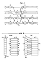
- FIG. 4 shows the signal flow for a "fast DCT” algorithm, where each of the circles in FIG. 4 (e.g., circle 17) represents an in-place rotation.
- in-place rotation we mean that the rotation operation is performed with a communication circuit that, as it feeds two inputs signals to the rotator from particular storage locations, the results (from the rotator) are placed back into the same storage locations. What is necessary, then, is to appropriately control the sequencing of signals to and from communications circuit 100 to accomplish the end results which are specified in FIG. 4 and summarized in Table 1 below.
- FIG. 5 presents a functional diagram of a communications circuit 100.
- circuit 100 comprises an addressable memory 121 and a nonaddressable memory 122.
- Memory 122 is primarily a serial memory. That is, input data is shifted into memory 122 at line 123, and transformed output signals are shifted out of memory 122 at line 124. This condition is depicted by the left side illustration of FIG. 5 under the heading "normal". While input data is being shifted into memory 122, memory 121 is engaged with rotator 300 and performs the in-place substitutions of rotator results for rotator input signals. This is easily achieved since memory 121 is addressable and arranged so that data from each storage address is fed back to itself at all addresses other than at the two selected ones.
- Table 2 shows the addressing sequence for memory 122 and the coefficients applied to rotator 300.
- the addresses and coefficients of Table 2 correspond to FIG. 4 designations.
- FIG. 4 reveals that any sequence is acceptable which insures that certain rotations do not precede certain other rotations. It may also be noted that the fast DCT of FIG. 4 is not the only possible "fast DCT" algorithm. To illustrate, FIG. 6 presents an algorithm that, in some sense, is more regular than the algorithm depicted in FIG. 4. The circles and numbers in FIG. 6 have the same meaning as in FIG. 4.
- FIG. 7 illustrates one communication circuit 100 embodiment for implementing the functional diagram of FIG. 5.
- Input signals Y0 and Y1 are applied to normalization units 110 and 120, and the outputs of normalization units 110 and 120 are applied to address multiplexers 111 and 112.
- Multiplexers 111 and 112 are responsive to address signals addr0 and addr1. These address signals are delivered to communication circuit 100 by Look-up table 200 and they follow the sequence defined, for example, in Table 2.
- Multiplexers 111 and 112 are conventional one-to-many selectors, in the sense that they cause input signals Y o and Y1 to appear on one output of the many outputs of multiplexers 111 and 112, respectively.
- Multiplexers 111 and 112 differ from conventional multiplexers in that with each output lead there is an associated control lead which identifies the output lead upon which signals are present. This lead enables the feeding back of signals from all of the registers that do not receive signals Y, as discussed in connection with FIG. 5.
- the outputs of multiplexers 111 and 112 are connected to a multi input-multi output memory block 130 which encompasses memories 121 and 122, and which comprises a plurality of storage blocks 131.
- Each storage block 131 has two inputs and two outputs, a "ready" control signal input, an enable control signal, and two registers.
- the outputs of multiplexer 111 are each connected to one input of a different storage block 131.
- the outputs of multiplexer 112 are each connected in parallel to the outputs of multiplexer 111.
- the other input of each storage block is connected to the one output of the previous storage block 131, forming thereby the input and output connections to the serial memory arrangement 122.
- the other outputs of storage block 131 are applied to address multiplexers 113 and 114, which are under control of addr0 and addr1 control signals.
- the output signals of multiplexers 113 and 114 (many-to-one) are the signals X0 and X1 that are applied to rotator 300.
- Signals X0 and X1 are either the input signal x or intermediate results terms as described by the signal flow diagram of FIG. 4.
- signals Y0 and Y1 are the computation results of the rotator which, at completion, are equal to y0 and y1.
- FIG. 8 depicts one realization for storage blocks 131. It includes registers 133 and 134, a double pole double throw switch 132, and a single pole double throw switch 135.
- the input signals from multiplexers 111 and 112 are applied to the input port of switch 135, and the enable signals from multiplexers 111 and 112 are applied to the control port of switch 135.
- the other input to switch 135 is obtained from the output of register 133, achieving thereby the signal feed-back capability.
- the output signal of switch 135 is applied to one input of switch 132, while the serial input of block 131 is applied to the other input of switch 132.
- Switch 132 is controlled by the "ready" control signal.
- the "ready" control signal is set so that the serial input is applied by switch 132 to register 134 and the other input (from switch 135) is applied to register 133.
- the output of register 133 is applied to multiplexers 113 and 114 (in addition to being applied to switch 135), while the output signal of register 134 is applied to the serial input of the next block 131.
- Normalization units 110 and 120 in FIG. 7 are necessary because the multiplication results of rotator 300 contain a number of bits that is equal to sum of the bits in the multiplier and the multiplicand (plus 1). This number has to be reduced to the number of bits in the multiplicand if the results are not to grow with each iteration. This can be done with simple truncation, but we suggest a normalization unit that clips infrequently occurring large values. Such clipping permits us to truncate fewer bits and thereby achieve a lower level of truncation errors.
- FIG. 9 depicts a simple realization for normalization units 110 and 120.
- Register 115 accepts the results of rotator 300, and a selected high significance output bits of register 115 are applied to detector 116.
- detector 116 sees all 0's or all 1's (the sign bit)
- a selected group of the next most significant bits of register 115 are passed through gate arrangement 117 to the multiplexers of FIG. 7. Otherwise, detector 117 blocks those output bits and replaces them with the sign bit.
- the orthogonal transform architecture is an iterative approach that requires a sequence of coefficients and "addr" addresses control signals in rapid succession.
- a conventional read-only memory and a counter is one solution for this function, but it is difficult to improve the speed of the address decoding in a standard ROM, and counters are more complicated than necessary.
- a serially-addressed read-only memory satisfies the requirements of the transform architecture and has the advantages of a shift-register intensive design.
- the read-only memory is embodied in block 56 which comprises a collection of signal lines, 51, 52, and 53 and activatable connection points 54.
- the signal lines are interleaved in accordance with the sequence 51, 52, 53, 52, 51, 52, ..., and connection points 54 connect (when activated) selected adjacent lines.
- Lines 51 are all connected to a first voltage source, V1, corresponding to logic level "1”
- lines 54 are all connected to a second voltage source, V0, corresponding to logic level"0”.
- Lines 52 form the output of the memory.
- Connection points 54 are conventional semiconductor switches under control of activation signals.
- connection points are arranged in groups, with each group consisting of a connection point associated with each line 52, and with all of the connection points being controlled by a single control signal.
- Control signals for the various groups are obtained from register 55, into which a pulse is inserted with each "ready" signal applied to look-up table 200. Successive words of memory are accessed as the "ready" pulse is shifted through register 55.
- Look-up table 200 in FIG. 1 also depicts an "inverse" control signal applied to the table. This signal provides for developing the inverse transform.
- the inverse transform can be realized with a second look-up table built into element 200, as shown in FIG. 11. All that is required is to employ two block 56 controlled by a register 55 and a multiplexer 57 that selects (under control of the "inverse" control signal) one of the two block 56 memories. This second look-up table permits specification of a different sequence of address coefficients.
- a candidate for the international low bit-rate video coder transform standard is a two-dimensional DCT on 8 x 8 blocks of pixels. This is separable into a one dimensional 8-point transform on each row of 8 pixels followed by a one dimensional 8-point transform on each column.
- Such a transform can be implemented, as shown in FIG. 12, with an orthogonal transform processor 501 cascaded with a transpose memory 502 and another orthogonal transform processor 501; or it can be implemented in a single orthogonal transform processor 501 where the memory contains 64 samples and the look-up table is arranged appropriately.
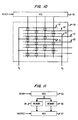
- FIG. 13 presents one approach to the realization of transpose memory 502. It comprises a two dimensional array of storage registers 503 that can be configured to shift in a horizontal or vertical raster-scan sequence. More particularly, each storage register 503 has a horizontal input and output, a vertical input and output, and a direction control input.
- the array of registers 503 is interconnected by having horizontal outputs within a row connected to horizontal inputs within the same row, and vertical outputs in a column connected to vertical inputs within the same column. This applies to all elements which are not in the first or last column or row.
- the vertical output in the last row of each column is connected to the vertical input of the first row in the next column and, similarly, the last horizontal output in each column is connected to the first horizontal input in the next row.
- the two inputs of the register in the first row and the first column are interconnected and comprise the input to transpose memory 502.
- the two outputs of the register in the last row and the last column are also interconnected and comprise the output of transpos
- each storage register 503 includes a register 504 and a selector 505.
- Selector 505 is responsive to the direction control signal which selects either the horizontal input or the vertical input. The selected input is applied to register 504, and the output of register 504 is applied to both the horizontal and the vertical outputs.
- the processor may contain more than one processing element, e.g., a rotator and a separate adder/subtractor unit which implements rotations of 45°, which will increase the processing speed of the unit by taking advantage of the parallelism in the algorithm.
- FIG. 1 depicts a communications circuit 100 which serves as an I/O interface and a storage means communicating with a processor element (rotator 300), by a simple extension of our invention one can employ a plurality of processor elements connected to the I/O interface and the storage means (considered as being embedded within rotator 300, or otherwise).
Landscapes
- Physics & Mathematics (AREA)
- Engineering & Computer Science (AREA)
- Mathematical Physics (AREA)
- General Physics & Mathematics (AREA)
- Theoretical Computer Science (AREA)
- Data Mining & Analysis (AREA)
- Computational Mathematics (AREA)
- Mathematical Analysis (AREA)
- Mathematical Optimization (AREA)
- Pure & Applied Mathematics (AREA)
- General Engineering & Computer Science (AREA)
- Databases & Information Systems (AREA)
- Software Systems (AREA)
- Discrete Mathematics (AREA)
- Algebra (AREA)
- Complex Calculations (AREA)
Applications Claiming Priority (2)
| Application Number | Priority Date | Filing Date | Title |
|---|---|---|---|
| US06/928,894 US4760543A (en) | 1986-11-10 | 1986-11-10 | Orthogonal transform processor |
| US928894 | 1986-11-10 |
Publications (3)
| Publication Number | Publication Date |
|---|---|
| EP0267729A2 EP0267729A2 (en) | 1988-05-18 |
| EP0267729A3 EP0267729A3 (en) | 1991-03-13 |
| EP0267729B1 true EP0267729B1 (en) | 1994-06-08 |
Family
ID=25456957
Family Applications (1)
| Application Number | Title | Priority Date | Filing Date |
|---|---|---|---|
| EP87309736A Expired - Lifetime EP0267729B1 (en) | 1986-11-10 | 1987-11-04 | An orthogonal transform processor |
Country Status (8)
| Country | Link |
|---|---|
| US (1) | US4760543A (es) |
| EP (1) | EP0267729B1 (es) |
| JP (1) | JPS63136167A (es) |
| KR (1) | KR920001618B1 (es) |
| CN (1) | CN87107679A (es) |
| CA (1) | CA1277036C (es) |
| DE (1) | DE3750017T2 (es) |
| ES (1) | ES2005021A6 (es) |
Families Citing this family (28)
| Publication number | Priority date | Publication date | Assignee | Title |
|---|---|---|---|---|
| US5424961A (en) * | 1988-03-04 | 1995-06-13 | Brust; Hans-Detlef | Process and system for measuring the temporal course of a periodic signal having high time resolution according to a "Boxcar-like" process |
| FR2639738B1 (fr) * | 1988-11-25 | 1992-05-07 | France Etat | Dispositif et procede a registres a decalage et a operateurs de permutation pour la transposition matricielle ligne-colonne |
| US5359549A (en) * | 1989-12-01 | 1994-10-25 | Ricoh Company, Ltd. | Orthogonal transformation processor for compressing information |
| US5268853A (en) * | 1989-12-01 | 1993-12-07 | Ricoh Company, Ltd. | Orthogonal transformation processor for compressing information |
| JP2646778B2 (ja) * | 1990-01-17 | 1997-08-27 | 日本電気株式会社 | ディジタル信号処理装置 |
| FR2657739B1 (fr) * | 1990-01-26 | 1992-05-07 | Sgc Thomson Microelectronics Sa | Serialiseur/deserialiseur. |
| US5126962A (en) * | 1990-07-11 | 1992-06-30 | Massachusetts Institute Of Technology | Discrete cosine transform processing system |
| EP0469855B1 (en) | 1990-07-31 | 1999-12-01 | Fujitsu Limited | Image data processing method and apparatus |
| US5875266A (en) * | 1990-07-31 | 1999-02-23 | Fujitsu Limited | Image data processing a method and apparatus |
| JP2646844B2 (ja) * | 1990-11-16 | 1997-08-27 | 日本電気株式会社 | 離散コサイン変換装置 |
| US5343501A (en) * | 1991-02-19 | 1994-08-30 | Matsushita Electric Industrial Co., Ltd. | Orthogonal transform apparatus for video signal processing |
| JP2964172B2 (ja) * | 1991-03-08 | 1999-10-18 | 富士通株式会社 | Dctマトリクス演算回路 |
| US5394349A (en) * | 1992-07-10 | 1995-02-28 | Xing Technology Corporation | Fast inverse discrete transform using subwords for decompression of information |
| US5339265A (en) * | 1992-08-31 | 1994-08-16 | University Of Maryland At College Park | Optimal unified architectures for the real-time computation of time-recursive discrete sinusoidal transforms |
| KR950000386B1 (ko) * | 1992-12-30 | 1995-01-16 | 재단법인 한국전자통신연구소 | 이산여현 변환회로 |
| US5345408A (en) * | 1993-04-19 | 1994-09-06 | Gi Corporation | Inverse discrete cosine transform processor |
| US5428567A (en) * | 1994-05-09 | 1995-06-27 | International Business Machines Corporation | Memory structure to minimize rounding/trunction errors for n-dimensional image transformation |
| US6310963B1 (en) | 1994-09-30 | 2001-10-30 | Sensormatic Electronics Corp | Method and apparatus for detecting an EAS (electronic article surveillance) marker using wavelet transform signal processing |
| US5623423A (en) * | 1994-12-12 | 1997-04-22 | Univ. Of Texas | Apparatus and method for video decoding |
| US5801979A (en) * | 1995-10-20 | 1998-09-01 | Matsushita Electric Corporation Of America | Carry logic that produces a carry value from NLSBs for a ROM accumulator in an inverse discrete cosine transform processor |
| US5805482A (en) * | 1995-10-20 | 1998-09-08 | Matsushita Electric Corporation Of America | Inverse discrete cosine transform processor having optimum input structure |
| US5867601A (en) * | 1995-10-20 | 1999-02-02 | Matsushita Electric Corporation Of America | Inverse discrete cosine transform processor using parallel processing |
| US6101523A (en) * | 1998-05-19 | 2000-08-08 | United Microelectronics Corp. | Method and apparatus for controlling calculation error |
| US6499045B1 (en) * | 1999-10-21 | 2002-12-24 | Xilinx, Inc. | Implementation of a two-dimensional wavelet transform |
| US7292730B1 (en) * | 1999-12-09 | 2007-11-06 | Intel Corporation | Two-dimensional inverse discrete cosine transforming |
| US6684235B1 (en) | 2000-11-28 | 2004-01-27 | Xilinx, Inc. | One-dimensional wavelet system and method |
| US7054897B2 (en) * | 2001-10-03 | 2006-05-30 | Dsp Group, Ltd. | Transposable register file |
| US10884707B1 (en) | 2019-06-27 | 2021-01-05 | Amazon Technologies, Inc. | Transpose operations using processing element array |
Family Cites Families (10)
| Publication number | Priority date | Publication date | Assignee | Title |
|---|---|---|---|---|
| FR2262350B1 (es) * | 1974-02-25 | 1976-12-03 | France Etat | |
| US4385363A (en) * | 1978-12-15 | 1983-05-24 | Compression Labs, Inc. | Discrete cosine transformer |
| US4293920A (en) * | 1979-09-04 | 1981-10-06 | Merola Pasquale A | Two-dimensional transform processor |
| JPS57146345A (en) * | 1981-03-04 | 1982-09-09 | Toshiba Corp | 3n-th degree orthogonal transformation and inverse transformation system |
| US4528641A (en) * | 1982-11-16 | 1985-07-09 | The United States Of America As Represented By The Secretary Of The Air Force | Variable radix processor |
| GB2141847B (en) * | 1983-05-06 | 1986-10-15 | Seiko Instr & Electronics | Matrix multiplication apparatus for graphic display |
| US4558351A (en) * | 1983-11-21 | 1985-12-10 | Rca Corporation | Hue correction circuit for a digital TV receiver |
| US4612626A (en) * | 1983-12-27 | 1986-09-16 | Motorola Inc. | Method of performing real input fast fourier transforms simultaneously on two data streams |
| FR2561011B1 (fr) * | 1984-03-09 | 1986-09-12 | Cit Alcatel | Processeur de calcul d'une transformee discrete inverse du cosinus |
| US4791590A (en) * | 1985-11-19 | 1988-12-13 | Cornell Research Foundation, Inc. | High performance signal processor |
-
1986
- 1986-11-10 US US06/928,894 patent/US4760543A/en not_active Expired - Lifetime
-
1987
- 1987-09-29 ES ES8702777A patent/ES2005021A6/es not_active Expired
- 1987-10-27 CA CA000550372A patent/CA1277036C/en not_active Expired - Fee Related
- 1987-11-04 DE DE3750017T patent/DE3750017T2/de not_active Expired - Fee Related
- 1987-11-04 EP EP87309736A patent/EP0267729B1/en not_active Expired - Lifetime
- 1987-11-09 CN CN198787107679A patent/CN87107679A/zh active Pending
- 1987-11-10 JP JP62282270A patent/JPS63136167A/ja active Pending
- 1987-11-10 KR KR1019870012639A patent/KR920001618B1/ko not_active IP Right Cessation
Also Published As
| Publication number | Publication date |
|---|---|
| ES2005021A6 (es) | 1989-02-16 |
| JPS63136167A (ja) | 1988-06-08 |
| EP0267729A2 (en) | 1988-05-18 |
| DE3750017T2 (de) | 1994-09-29 |
| CN87107679A (zh) | 1988-08-31 |
| DE3750017D1 (de) | 1994-07-14 |
| US4760543A (en) | 1988-07-26 |
| KR920001618B1 (ko) | 1992-02-20 |
| KR880006617A (ko) | 1988-07-23 |
| CA1277036C (en) | 1990-11-27 |
| EP0267729A3 (en) | 1991-03-13 |
Similar Documents
| Publication | Publication Date | Title |
|---|---|---|
| EP0267729B1 (en) | An orthogonal transform processor | |
| KR100373222B1 (ko) | 반도체집적회로 | |
| US6041340A (en) | Method for configuring an FPGA for large FFTs and other vector rotation computations | |
| US6021423A (en) | Method for parallel-efficient configuring an FPGA for large FFTS and other vector rotation computations | |
| Wold et al. | Pipeline and parallel-pipeline FFT processors for VLSI implementations | |
| US4821224A (en) | Method and apparatus for processing multi-dimensional data to obtain a Fourier transform | |
| EP0353223B1 (en) | Two-dimensional discrete cosine transform processor | |
| Madisetti et al. | A 100 MHz 2-D 8/spl times/8 DCT/IDCT processor for HDTV applications | |
| US4777614A (en) | Digital data processor for matrix-vector multiplication | |
| US5481487A (en) | Transpose memory for DCT/IDCT circuit | |
| EP2017743B1 (en) | High speed and efficient matrix multiplication hardware module | |
| US5179714A (en) | Parallel bit serial data processor | |
| EP0847552B1 (en) | An apparatus for performing multiply-add operations on packed data | |
| AU5412694A (en) | Scalable dimensionless array | |
| EP0953175B1 (en) | Method and apparatus for fft computation | |
| Mehlhorn et al. | Area—Time optimal VLSI integer multiplier with minimum computation time | |
| Lim et al. | A serial-parallel architecture for two-dimensional discrete cosine and inverse discrete cosine transforms | |
| US5010511A (en) | Digit-serial linear combining apparatus useful in dividers | |
| US6460061B1 (en) | 2-dimensional discrete cosine transform using a polynomial transform | |
| US5793658A (en) | Method and apparatus for viedo compression and decompression using high speed discrete cosine transform | |
| Sikström et al. | A high speed 2-D discrete cosine transform chip | |
| Guo | An efficient parallel adder based design for one dimensional discrete Fourier transform | |
| Demassieux et al. | Orthogonal transforms | |
| Baghaie et al. | An efficient new systolic architecture for the solution of discrete Fourier transform | |
| Ward et al. | A systolic implementation of the Winograd Fourier transform algorithm |
Legal Events
| Date | Code | Title | Description |
|---|---|---|---|
| PUAI | Public reference made under article 153(3) epc to a published international application that has entered the european phase |
Free format text: ORIGINAL CODE: 0009012 |
|
| AK | Designated contracting states |
Kind code of ref document: A2 Designated state(s): DE FR GB IT NL SE |
|
| PUAL | Search report despatched |
Free format text: ORIGINAL CODE: 0009013 |
|
| AK | Designated contracting states |
Kind code of ref document: A3 Designated state(s): DE FR GB IT NL SE |
|
| 17P | Request for examination filed |
Effective date: 19910905 |
|
| 17Q | First examination report despatched |
Effective date: 19921222 |
|
| GRAA | (expected) grant |
Free format text: ORIGINAL CODE: 0009210 |
|
| AK | Designated contracting states |
Kind code of ref document: B1 Designated state(s): DE FR GB IT NL SE |
|
| ITF | It: translation for a ep patent filed | ||
| RAP4 | Party data changed (patent owner data changed or rights of a patent transferred) |
Owner name: AT&T CORP. |
|
| ET | Fr: translation filed | ||
| REF | Corresponds to: |
Ref document number: 3750017 Country of ref document: DE Date of ref document: 19940714 |
|
| EAL | Se: european patent in force in sweden |
Ref document number: 87309736.4 |
|
| PLBE | No opposition filed within time limit |
Free format text: ORIGINAL CODE: 0009261 |
|
| STAA | Information on the status of an ep patent application or granted ep patent |
Free format text: STATUS: NO OPPOSITION FILED WITHIN TIME LIMIT |
|
| NLT1 | Nl: modifications of names registered in virtue of documents presented to the patent office pursuant to art. 16 a, paragraph 1 |
Owner name: AT&T CORP. TE NEW YORK, NEW YORK, VER. ST. V. AM. |
|
| 26N | No opposition filed | ||
| PGFP | Annual fee paid to national office [announced via postgrant information from national office to epo] |
Ref country code: SE Payment date: 20011002 Year of fee payment: 15 |
|
| PGFP | Annual fee paid to national office [announced via postgrant information from national office to epo] |
Ref country code: FR Payment date: 20011022 Year of fee payment: 15 |
|
| PGFP | Annual fee paid to national office [announced via postgrant information from national office to epo] |
Ref country code: NL Payment date: 20011026 Year of fee payment: 15 |
|
| PGFP | Annual fee paid to national office [announced via postgrant information from national office to epo] |
Ref country code: GB Payment date: 20011116 Year of fee payment: 15 |
|
| PGFP | Annual fee paid to national office [announced via postgrant information from national office to epo] |
Ref country code: DE Payment date: 20011230 Year of fee payment: 15 |
|
| REG | Reference to a national code |
Ref country code: GB Ref legal event code: IF02 |
|
| PG25 | Lapsed in a contracting state [announced via postgrant information from national office to epo] |
Ref country code: GB Free format text: LAPSE BECAUSE OF NON-PAYMENT OF DUE FEES Effective date: 20021104 |
|
| PG25 | Lapsed in a contracting state [announced via postgrant information from national office to epo] |
Ref country code: SE Free format text: LAPSE BECAUSE OF NON-PAYMENT OF DUE FEES Effective date: 20021105 |
|
| PG25 | Lapsed in a contracting state [announced via postgrant information from national office to epo] |
Ref country code: NL Free format text: LAPSE BECAUSE OF NON-PAYMENT OF DUE FEES Effective date: 20030601 |
|
| PG25 | Lapsed in a contracting state [announced via postgrant information from national office to epo] |
Ref country code: DE Free format text: LAPSE BECAUSE OF NON-PAYMENT OF DUE FEES Effective date: 20030603 |
|
| GBPC | Gb: european patent ceased through non-payment of renewal fee | ||
| EUG | Se: european patent has lapsed | ||
| PG25 | Lapsed in a contracting state [announced via postgrant information from national office to epo] |
Ref country code: FR Free format text: LAPSE BECAUSE OF NON-PAYMENT OF DUE FEES Effective date: 20030731 |
|
| NLV4 | Nl: lapsed or anulled due to non-payment of the annual fee |
Effective date: 20030601 |
|
| REG | Reference to a national code |
Ref country code: FR Ref legal event code: ST |
|
| PG25 | Lapsed in a contracting state [announced via postgrant information from national office to epo] |
Ref country code: IT Free format text: LAPSE BECAUSE OF NON-PAYMENT OF DUE FEES;WARNING: LAPSES OF ITALIAN PATENTS WITH EFFECTIVE DATE BEFORE 2007 MAY HAVE OCCURRED AT ANY TIME BEFORE 2007. THE CORRECT EFFECTIVE DATE MAY BE DIFFERENT FROM THE ONE RECORDED. Effective date: 20051104 |