EP0266572B1 - Semiconductor memory device having a plurality of memory cells of single transistor type - Google Patents
Semiconductor memory device having a plurality of memory cells of single transistor type Download PDFInfo
- Publication number
- EP0266572B1 EP0266572B1 EP87114591A EP87114591A EP0266572B1 EP 0266572 B1 EP0266572 B1 EP 0266572B1 EP 87114591 A EP87114591 A EP 87114591A EP 87114591 A EP87114591 A EP 87114591A EP 0266572 B1 EP0266572 B1 EP 0266572B1
- Authority
- EP
- European Patent Office
- Prior art keywords
- cell
- trench
- semiconductor
- source
- drain regions
- Prior art date
- Legal status (The legal status is an assumption and is not a legal conclusion. Google has not performed a legal analysis and makes no representation as to the accuracy of the status listed.)
- Expired - Lifetime
Links
- 239000004065 semiconductor Substances 0.000 title claims description 39
- 239000003990 capacitor Substances 0.000 claims description 56
- 239000012535 impurity Substances 0.000 claims description 26
- 239000000758 substrate Substances 0.000 claims description 21
- 229910052710 silicon Inorganic materials 0.000 claims description 13
- 239000010703 silicon Substances 0.000 claims description 13
- XUIMIQQOPSSXEZ-UHFFFAOYSA-N Silicon Chemical compound [Si] XUIMIQQOPSSXEZ-UHFFFAOYSA-N 0.000 description 12
- VYPSYNLAJGMNEJ-UHFFFAOYSA-N Silicium dioxide Chemical compound O=[Si]=O VYPSYNLAJGMNEJ-UHFFFAOYSA-N 0.000 description 3
- 230000010354 integration Effects 0.000 description 3
- 229910021420 polycrystalline silicon Inorganic materials 0.000 description 3
- 229910052814 silicon oxide Inorganic materials 0.000 description 3
- 230000015556 catabolic process Effects 0.000 description 2
- 230000012447 hatching Effects 0.000 description 2
- 238000009751 slip forming Methods 0.000 description 2
- 238000009413 insulation Methods 0.000 description 1
- 230000002093 peripheral effect Effects 0.000 description 1
Images


Classifications
-
- G—PHYSICS
- G11—INFORMATION STORAGE
- G11C—STATIC STORES
- G11C11/00—Digital stores characterised by the use of particular electric or magnetic storage elements; Storage elements therefor
- G11C11/21—Digital stores characterised by the use of particular electric or magnetic storage elements; Storage elements therefor using electric elements
- G11C11/34—Digital stores characterised by the use of particular electric or magnetic storage elements; Storage elements therefor using electric elements using semiconductor devices
- G11C11/40—Digital stores characterised by the use of particular electric or magnetic storage elements; Storage elements therefor using electric elements using semiconductor devices using transistors
- G11C11/401—Digital stores characterised by the use of particular electric or magnetic storage elements; Storage elements therefor using electric elements using semiconductor devices using transistors forming cells needing refreshing or charge regeneration, i.e. dynamic cells
- G11C11/403—Digital stores characterised by the use of particular electric or magnetic storage elements; Storage elements therefor using electric elements using semiconductor devices using transistors forming cells needing refreshing or charge regeneration, i.e. dynamic cells with charge regeneration common to a multiplicity of memory cells, i.e. external refresh
- G11C11/404—Digital stores characterised by the use of particular electric or magnetic storage elements; Storage elements therefor using electric elements using semiconductor devices using transistors forming cells needing refreshing or charge regeneration, i.e. dynamic cells with charge regeneration common to a multiplicity of memory cells, i.e. external refresh with one charge-transfer gate, e.g. MOS transistor, per cell
-
- H—ELECTRICITY
- H10—SEMICONDUCTOR DEVICES; ELECTRIC SOLID-STATE DEVICES NOT OTHERWISE PROVIDED FOR
- H10B—ELECTRONIC MEMORY DEVICES
- H10B12/00—Dynamic random access memory [DRAM] devices
- H10B12/30—DRAM devices comprising one-transistor - one-capacitor [1T-1C] memory cells
- H10B12/37—DRAM devices comprising one-transistor - one-capacitor [1T-1C] memory cells the capacitor being at least partially in a trench in the substrate
- H10B12/373—DRAM devices comprising one-transistor - one-capacitor [1T-1C] memory cells the capacitor being at least partially in a trench in the substrate the capacitor extending under or around the transistor
Definitions
- the present invention relates to a semiconductor memory device having a plurality of memory cells of single transistor type, and more particularly to the memory cell having a trench capacitor.
- a semiconductor memory device having a new single transistor type memory cell constituted by one transistor and one storage capacitor was proposed in TECHNICAL DIGEST of IEDM, 1984, pp 240 to 243, by S. Nakajima et al. entitled "AN ISOLATION-MERGED VERTICAL CAPACITOR CELL FOR LARGE CAPACITY DRAM".
- a trench for forming the capacitor is provided in a semiconductor substrate having an uniform impurity concentration from the major surface into the inner portion thereof, and surrounds the transistor forming region of the substrate.
- a cell plate is provided in the trench and capacitor electrodes are provided between the side walls of the trench and the cell plate, respectively, such that a first MOS capacitor is formed between the side wall of the trench and the capacitor electrode, and a second MOS capacitor is formed between the capacitor electrode and the cell plate.
- Source and drain regions of the transistor are formed in the transistor forming region surrounded by the trench. One of the source and drain regions is connected to the capacitor electrode at an upper side portion of the trench and the other of the source and drain regions is connected to a bit line at a surface portion located within the surface of the transistor forming region and separated from the trench.
- the memory cell can realize a large amount of storage capacitance because the first and second MOS capacitors surround the transistor forming region.
- the cell plate to which a constant voltage such as ground potential is applied, surrounds each memory cell. Therefore, an interference between memory cells can be avoided even if a conventional thick field insulating layer would not be formed therebetween.
- the bit line is connected to the source or drain region of the transistor at the portion which is located within the surface of the transistor forming region and separated from the trench. Therefore, a miniaturization of the memory cell in more extent, that is, a higher integration of the memory device cannot be realized.
- the impurity concentration of the substrate cannot be a high level because of obtaining a necessary breakdown voltage of the PN junction between the source, drain regions and the substrate.
- an inversion layer is apt to be produced along the side wall of the trench when a high voltage is applied to the capacitor electrode. Consequently, the information reservation characteristic of the memory cell is deteriorated by a leakage current between the inversion layer and the bit line via the source or drain region to which the bit line is connected.
- a semiconductor memory device having a plurality of memory cells comprising a semiconductor substrate of one conductivity type, a plurality of cell sections of said substrate, each of said cell sections having a rectangular shape in the plan view, a trench formed in said substrate and surrounding each of said cell sections such that the side wall of said trench delineates said rectangular shape in the plan view of said cell sections, capacitor electrodes formed in said trench and facing to said side wall of said trench and surrounding said rectangular shape, first insulating films provided between said side walls and said capacitor electrodes, second insulating films provided on said capacitor electrodes, a common cell plate provided on said second insulating films such that said common cell plate faces to respective said capacitor electrodes via said second insulating films, source and drain regions of the opposite conductivity type formed in said cell sections, one of said source and drain regions being provided along one side of each of said cell sections and connected to said capacitor electrode and the other of said source and drain regions being provided along another side of each of said cell sections, and a bit line electrically connected to said other of said source and drain regions
- the impurity concentration of the semiconductor body is favorably 1 ⁇ 1018 atoms/cm3 or more, and to obtain a sufficient breakdown voltage of source and drain regions of the transistor with a practical view, the semiconductor layer has favorably an impurity concentration ranging from 1 ⁇ 1015 atoms/cm3 to 5 ⁇ 1017 atoms/cm3 and the thickness ranging from 1 ⁇ m to 3 ⁇ m.
- a trench 110 is formed in a P-type substrate 111 having an uniform impurity concentration from the upper surface of the substrate to the inner portion thereof and surrounds a cell section 105 of the substrate in which a switching transistor is provided.
- a capacitor electrode 113 is formed on the side wall via a first insulating film 119 such that a first MOS capacitor is constituted by the substrate, that is, the side wall, the first insulating film and the capacitor electrode. Further, a common cell plate 114, to which a constant voltage such as earth potential is applied, is provided on the capacitor electrode via a second insulating film 118 to form a second MOS capacitor.
- the storage capacitor of the memory cell consist of the first and second MOS capacitors.
- Capacitor electrodes 115, 116, 117 and 118 of adjacent memory cells are provided in the same manner as the capacitor electrode 113, and the cell plate 114 is also employed as a common electrode for the adjacent memory cells.
- a pair of N-type impurity regions 120, 121 are formed in the upper surface of the substrate, and one of them is used as a source region of a transistor of the memor y cell and the other is used as a drain region of the transistor.
- a gate electrode 123 ⁇ which may be a part of a word line 123 is formed via a gate insulation film 125 ⁇ .
- the N-type impurity region 120 is connected to the capacitor electrode 113 at an upper side part 108 of the trench, and a bit line 124 is connected to the N-type impurity region 121 through a contact hole 109 provided in an insulating layer 125 at a contact portion 107 of, for example, 1.2 ⁇ m ⁇ 1.2 ⁇ m which is located in the surface of the cell region 105 and separated from the trench 110.
- a contact hole 109 provided in an insulating layer 125 at a contact portion 107 of, for example, 1.2 ⁇ m ⁇ 1.2 ⁇ m which is located in the surface of the cell region 105 and separated from the trench 110.
- an inversion layer (N type layer) 106 is apt to be produced along the side wall of the trench when a high positive voltage of +5 volt, for example, is applied to the capacitor electrode 113, and therefore, an information stored in the capacitor flows unfavorably to the bit line through the N-type impurity region 121. Further, the whole area of the contact portion 107 is provided on the N-type impurity region 121. Therefore, a high integration density of the device cannot be expected.
- a P-type semiconductor substrate 10 is composed by a P-type silicon body 11 having the impurity concentration of 1 ⁇ 1019 atoms/cm3 and a P-type epitaxial silicon layer 12 having the impurity concentration of 1 ⁇ 1017 atoms/cm3 formed on the silicon body, and a trench 60 having the width of 1.0 ⁇ m and the depth of 5.0 ⁇ m is formed in the substrate 10 from the upper surface of the silicon layer 12 into the silicon body 11.
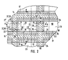
- the trench 60 has a grid-like shape in the plan view (Fig. 2) such that it surrounds each of cell sections 50 of the substrate.
- the cell section 50 has a rectangular plan shape of 2.0 ⁇ m ⁇ 1.5 ⁇ m, for example,surrounded by four straight edges 70, 71, 72, 73 which are delineated by the trench 60.
- An insulating film 32 is provided on the bottom of the trench, and a first insulating films 30 made of thermal silicon oxide and having the thickness of 5 nm to 30 nm are formed on lower side walls 40 of the trench 60 at the silicon body 11 such that each of the first insulating films 30 surrounds each of the cell sections 50 at the silicon body portion.
- the first insulating film 30 may extends on an upper side wall 41 at the side 70 as shown in Fig. 3A.
- Capacitor electrode 13 of N-type polycrystalline silicon is formed on the first insulating film 30 and surrounds the cell section 50 at the silicon body portion, and only at the side 70 the capacitor electrode 13 extends upwardly.
- a first MOS capacitor is constituted by the side wall 40 of the trench 60 at the silicon body 11 to which earth potential or -2 volt is applied, the first insulating film 30 and the capacitor electrode 13.
- Capacitor electrodes 15, 16, 17, 18 for forming MOS capacitors of the adjacent memory cells are formed by the same manner as the capacitor electrode 13.
- Second insulating films 31 made of thermal silicon oxide and having the thickness of 5 nm to 30 nm are formed on the capacitor electrodes, and a common cell plate 14 made of polycrystalline silicon and having a grid-like shape in the plan view is formed on the second insulating films 31.
- the ring shape capacitor electrodes are represented by right-upward hatching and the grid-like shape cell plate is represented by right-downward hatching
- the cell plate 14 is supplied with constant voltage such as earth potential through a wiring layer (not shown) connected to the cell plate at a peripheral portion of the substrate outside the memory section, and used as a common electrode for the plurality of memory cells.
- a second MOS capacitor is constituted by the cell plate 14, the second insulating film 31 and the capacitor electrode 13, 15, 16, 17 or 18, and the storage capacitor of the memory cell is composed by the first and second MOS capacitors.
- An insulating layer 19 such as CVD silicon oxide is continuously formed at the upper part of the trench 60.
- a pair of N-type impurity regions 20, 21 is formed on the upper surface of the silicon layer 12 in each cell section 50, and one is the source region of the switching transistor and the other being the drain region.
- the impurity region 20 is connected to the capacitor electrode 13 through an upper side part 39 of the trench at the side 70.
- a plurality of conductive layers 22 (only one layer is shown in Figs.) are selectively formed at the upper part of the trench along the side 71 of the cell section 50.
- the conductive layer 22 may be made of-N-type polycrystalline silicon and connected to the N-type impurity region 21 and also to an N-type impurity region 21' of the adjacent memory cell.
- the bit line 24 is connected to the conductive layer 22 and edges of the impurity regions 21, 21' at a contact area 36 of 1.2 ⁇ m ⁇ 1.2 ⁇ m through a contact hole 37 provided in an insulating layer 25.
- a gate electrode 23' of the switching transistor is formed on the channel region between the impurity regions 20, 21 via a gate insulating film 25', and the gate electrode 23' may be continuously formed with the word line 23.
- the inversion layer of N-type is hardly produced along the lower side wall 40 because the lower side wall 40 is formed by the silicon body 11 of high impurity concentration. Further, the capacitor electrode 13 is free from above the upper side wall 41 at the sides 71, 72, 73. Therefore, even if the inversion layer would be produced along the lower side wall when a high voltage such as +5 volt is applied to the capacitor electrode, the inversion layer is cut at the upper side wall 41. Consequently, an information stored in the capacitor is never flown to the bit line 24 through the N-type impurity region 21.
- an inversion layer provided in the upper side wall 41 at the side 70 is not the question because the inversion layer is only connected to the N-type impurity region 20 which is not directly contacted to the bit line 24 but interposed the channel region therebetween.
- the bit line 24 is connected to the conductive layer 22 on the trench. Therefore, the occupied area of the cell section, that is, the transistor forming area can be reduced and the integrated density of the device can be enhanced. More particularly, the area of the memory cell of the present invention can be about two third (2/3) of the prior art structure shown in Fig. 1.
- Figs. 4A, 4B in which same elements as those in Fig. 2 and Figs. 3A, 3B are indicated by the same reference numerals.
- the difference in the embodiment from the first embodiment resides in that an enlarged part 14 ⁇ is continuously provided to the cell plate 14 such that the enlarged part 14 ⁇ faces to the upper side wall 41 of the silicon layer 12 at the three side 71, 72, 73 and a thin insulating film 19 ⁇ which has nearly same thickness as the first insulating film 30 is interposed between the enlarged part 14 ⁇ and the upper side wall 41.
- the leakage of the information from the first MOS capacitor to the bit line is more securely prevented at the side wall 41 when a low voltage such as earth potential is applied to the cell plate 14, 14 ⁇ .
Landscapes
- Engineering & Computer Science (AREA)
- Microelectronics & Electronic Packaging (AREA)
- Computer Hardware Design (AREA)
- Semiconductor Memories (AREA)
Description
- The present invention relates to a semiconductor memory device having a plurality of memory cells of single transistor type, and more particularly to the memory cell having a trench capacitor.
- A semiconductor memory device according to the preamble part of claim 1 and having a new single transistor type memory cell constituted by one transistor and one storage capacitor was proposed in TECHNICAL DIGEST of IEDM, 1984, pp 240 to 243, by S. Nakajima et al. entitled "AN ISOLATION-MERGED VERTICAL CAPACITOR CELL FOR LARGE CAPACITY DRAM". In the memory cell, a trench for forming the capacitor is provided in a semiconductor substrate having an uniform impurity concentration from the major surface into the inner portion thereof, and surrounds the transistor forming region of the substrate. A cell plate is provided in the trench and capacitor electrodes are provided between the side walls of the trench and the cell plate, respectively, such that a first MOS capacitor is formed between the side wall of the trench and the capacitor electrode, and a second MOS capacitor is formed between the capacitor electrode and the cell plate. Source and drain regions of the transistor are formed in the transistor forming region surrounded by the trench. One of the source and drain regions is connected to the capacitor electrode at an upper side portion of the trench and the other of the source and drain regions is connected to a bit line at a surface portion located within the surface of the transistor forming region and separated from the trench.
- The memory cell can realize a large amount of storage capacitance because the first and second MOS capacitors surround the transistor forming region. The cell plate, to which a constant voltage such as ground potential is applied, surrounds each memory cell. Therefore, an interference between memory cells can be avoided even if a conventional thick field insulating layer would not be formed therebetween.
- However, in the memory cell, the bit line is connected to the source or drain region of the transistor at the portion which is located within the surface of the transistor forming region and separated from the trench. Therefore, a miniaturization of the memory cell in more extent, that is, a higher integration of the memory device cannot be realized. Further, the impurity concentration of the substrate cannot be a high level because of obtaining a necessary breakdown voltage of the PN junction between the source, drain regions and the substrate. In this case, an inversion layer is apt to be produced along the side wall of the trench when a high voltage is applied to the capacitor electrode. Consequently, the information reservation characteristic of the memory cell is deteriorated by a leakage current between the inversion layer and the bit line via the source or drain region to which the bit line is connected.
- Accordingly, it is an object of the present invention to provide an effective memory device in which the integration can be enhanced and the information reservation characteristic is never deteriorated by leakage current.
- This object is achieved by a semiconductor memory device having a plurality of memory cells comprising a semiconductor substrate of one conductivity type, a plurality of cell sections of said substrate, each of said cell sections having a rectangular shape in the plan view, a trench formed in said substrate and surrounding each of said cell sections such that the side wall of said trench delineates said rectangular shape in the plan view of said cell sections, capacitor electrodes formed in said trench and facing to said side wall of said trench and surrounding said rectangular shape, first insulating films provided between said side walls and said capacitor electrodes, second insulating films provided on said capacitor electrodes, a common cell plate provided on said second insulating films such that said common cell plate faces to respective said capacitor electrodes via said second insulating films, source and drain regions of the opposite conductivity type formed in said cell sections, one of said source and drain regions being provided along one side of each of said cell sections and connected to said capacitor electrode and the other of said source and drain regions being provided along another side of each of said cell sections, and a bit line electrically connected to said other of said source and drain regions, wherein said semiconductor substrate includes a semiconductor body of said one conductivity type and a semiconductor layer of said one conductivity type having a lower impurity concentration than that of said semiconductor body and formed on said semiconductor body and in which said source and drain regions are formed; said trench is formed from the surface of said semiconductor layer into said semiconductor body through said semiconductor layer such that said side walls of said trench are constituted by lower side walls of said semiconductor body and upper side walls of said semiconductor layer; each of said capacitor electrodes faces both said upper and lower side walls of said trench at said one side of said cell section via said first insulating film and faces only said lower side wall at said another side of said cell section via said first insulating film such that said capacitor electrode is free from above said upper side wall at said another side of said cell section; and a conductive layer provided at the upper part of said trench along said another side of said cell section and connected to said other of said source and drain regions and to said bit line such that said bit line is electrically connected to said other of said source and drain regions through said conductive layer. To avoid the occurrence of an inversion layer along the trench, the impurity concentration of the semiconductor body is favorably 1 × 10¹⁸ atoms/cm³ or more, and to obtain a sufficient breakdown voltage of source and drain regions of the transistor with a practical view, the semiconductor layer has favorably an impurity concentration ranging from 1 × 10¹⁵ atoms/cm³ to 5 × 10¹⁷ atoms/cm³ and the thickness ranging from 1 µm to 3 µm.
-
- Figs. 1A and 1B are cross-sectional views showing a semiconductor memory device in a prior art taken along the bit line and the word line, respectively;
- Fig. 2 is a plan view showing a first embodiment of the present invention;
- Figs. 3A and 3B are cross-sectional views of the first embodiment taken along lines A-A' and B-B', respectively, in Fig. 2 as viewed in the directions of arrows; and
- Figs. 4A and 4B are cross-sectional views showing a second embodiment of the present invention which correspond to Figs. 3A and 3B, respectively.
- Referring to Figs. 1A and 1B, a
trench 110 is formed in a P-type substrate 111 having an uniform impurity concentration from the upper surface of the substrate to the inner portion thereof and surrounds acell section 105 of the substrate in which a switching transistor is provided. - In the
trench 110, acapacitor electrode 113 is formed on the side wall via a firstinsulating film 119 such that a first MOS capacitor is constituted by the substrate, that is, the side wall, the first insulating film and the capacitor electrode. Further, acommon cell plate 114, to which a constant voltage such as earth potential is applied, is provided on the capacitor electrode via a secondinsulating film 118 to form a second MOS capacitor. The storage capacitor of the memory cell consist of the first and second MOS capacitors.Capacitor electrodes capacitor electrode 113, and thecell plate 114 is also employed as a common electrode for the adjacent memory cells. A pair of N-type impurity regions impurity regions word line 123 is formed via a gate insulation film 125ʹ. The N-type impurity region 120 is connected to thecapacitor electrode 113 at anupper side part 108 of the trench, and abit line 124 is connected to the N-type impurity region 121 through acontact hole 109 provided in aninsulating layer 125 at acontact portion 107 of, for example, 1.2 µm × 1.2 µm which is located in the surface of thecell region 105 and separated from thetrench 110. In the structure shown in Fig. 1, an inversion layer (N type layer) 106 is apt to be produced along the side wall of the trench when a high positive voltage of +5 volt, for example, is applied to thecapacitor electrode 113, and therefore, an information stored in the capacitor flows unfavorably to the bit line through the N-type impurity region 121. Further, the whole area of thecontact portion 107 is provided on the N-type impurity region 121. Therefore, a high integration density of the device cannot be expected. - Referring to Fig. 2 and Figs. 3A, 3B, a P-
type semiconductor substrate 10 is composed by a P-type silicon body 11 having the impurity concentration of 1 × 10¹⁹ atoms/cm³ and a P-typeepitaxial silicon layer 12 having the impurity concentration of 1 × 10¹⁷ atoms/cm³ formed on the silicon body, and atrench 60 having the width of 1.0 µm and the depth of 5.0 µm is formed in thesubstrate 10 from the upper surface of thesilicon layer 12 into thesilicon body 11. Thetrench 60 has a grid-like shape in the plan view (Fig. 2) such that it surrounds each ofcell sections 50 of the substrate. More particularly, thecell section 50 has a rectangular plan shape of 2.0 µm × 1.5 µm, for example,surrounded by fourstraight edges trench 60. Aninsulating film 32 is provided on the bottom of the trench, and a firstinsulating films 30 made of thermal silicon oxide and having the thickness of 5 nm to 30 nm are formed onlower side walls 40 of thetrench 60 at thesilicon body 11 such that each of the firstinsulating films 30 surrounds each of thecell sections 50 at the silicon body portion. The firstinsulating film 30 may extends on anupper side wall 41 at theside 70 as shown in Fig. 3A.Capacitor electrode 13 of N-type polycrystalline silicon is formed on the firstinsulating film 30 and surrounds thecell section 50 at the silicon body portion, and only at theside 70 thecapacitor electrode 13 extends upwardly. A first MOS capacitor is constituted by theside wall 40 of thetrench 60 at thesilicon body 11 to which earth potential or -2 volt is applied, the firstinsulating film 30 and thecapacitor electrode 13.Capacitor electrodes capacitor electrode 13. Secondinsulating films 31 made of thermal silicon oxide and having the thickness of 5 nm to 30 nm are formed on the capacitor electrodes, and acommon cell plate 14 made of polycrystalline silicon and having a grid-like shape in the plan view is formed on the secondinsulating films 31. In Fig. 2, the ring shape capacitor electrodes are represented by right-upward hatching and the grid-like shape cell plate is represented by right-downward hatching Thecell plate 14 is supplied with constant voltage such as earth potential through a wiring layer (not shown) connected to the cell plate at a peripheral portion of the substrate outside the memory section, and used as a common electrode for the plurality of memory cells. A second MOS capacitor is constituted by thecell plate 14, the secondinsulating film 31 and thecapacitor electrode insulating layer 19 such as CVD silicon oxide is continuously formed at the upper part of thetrench 60. A pair of N-type impurity regions silicon layer 12 in eachcell section 50, and one is the source region of the switching transistor and the other being the drain region. Theimpurity region 20 is connected to thecapacitor electrode 13 through anupper side part 39 of the trench at theside 70. A plurality of conductive layers 22 (only one layer is shown in Figs.) are selectively formed at the upper part of the trench along theside 71 of thecell section 50. Theconductive layer 22 may be made of-N-type polycrystalline silicon and connected to the N-type impurity region 21 and also to an N-type impurity region 21' of the adjacent memory cell. Thebit line 24 is connected to theconductive layer 22 and edges of theimpurity regions 21, 21' at acontact area 36 of 1.2 µm × 1.2 µm through acontact hole 37 provided in aninsulating layer 25. A gate electrode 23' of the switching transistor is formed on the channel region between theimpurity regions word line 23. - According to the present invention, the inversion layer of N-type is hardly produced along the
lower side wall 40 because thelower side wall 40 is formed by thesilicon body 11 of high impurity concentration. Further, thecapacitor electrode 13 is free from above theupper side wall 41 at thesides upper side wall 41. Consequently, an information stored in the capacitor is never flown to thebit line 24 through the N-type impurity region 21. It is to be noted that an inversion layer provided in theupper side wall 41 at theside 70 is not the question because the inversion layer is only connected to the N-type impurity region 20 which is not directly contacted to thebit line 24 but interposed the channel region therebetween. Moreover, thebit line 24 is connected to theconductive layer 22 on the trench. Therefore, the occupied area of the cell section, that is, the transistor forming area can be reduced and the integrated density of the device can be enhanced. More particularly, the area of the memory cell of the present invention can be about two third (2/3) of the prior art structure shown in Fig. 1. - Referring to Figs. 4A, 4B, in which same elements as those in Fig. 2 and Figs. 3A, 3B are indicated by the same reference numerals. The difference in the embodiment from the first embodiment resides in that an enlarged part 14ʹ is continuously provided to the
cell plate 14 such that the enlarged part 14ʹ faces to theupper side wall 41 of thesilicon layer 12 at the threeside film 30 is interposed between the enlarged part 14ʹ and theupper side wall 41. According to the embodiment, the leakage of the information from the first MOS capacitor to the bit line is more securely prevented at theside wall 41 when a low voltage such as earth potential is applied to thecell plate 14, 14ʹ.
Claims (5)
- A semiconductor memory device having a plurality of memory cells comprising a semiconductor substrate (10) of one conductivity type, a plurality of cell sections (50) of said substrate (10), each of said cell sections (50) having a rectangular shape in the plan view, a trench (60) formed in said substrate (10) and surrounding each of said cell sections (50) such that the side wall of said trench (60) delineates said rectangular shape in the plan view of said cell sections (50), capacitor electrodes (13,15,16,17,18) formed in said trench (60) and facing to said side wall of said trench (60) and surrounding said rectangular shape, first insulating films (30) provided between said side walls and said capacitor electrodes (13,15,16,17,18), second insulating films (31) provided on said capacitor electrodes (13,15,16,17,18), a common cell plate (14) provided on said second insulating films (31) such that said common cell plate (14) faces to respective said capacitor electrodes (13,15,16,17,18) via said second insulating films (31), source and drain regions (20,21) of the opposite conductivity type formed in said cell sections (50), one (20) of said source and drain regions being provided along one side of each of said cell sections (50) and connected to said capacitor electrode (13,15,16,17,18) and the other (21) of said source and drain regions being provided along another side of each of said cell sections (50), and a bit line (24) electrically connected to said other (21) of said source and drain regions,
characterized in that said semiconductor substrate (10) includes a semiconductor body (11) of said one conductivity type and a semiconductor layer (12) of said one conductivity type having a lower impurity concentration than that of said semiconductor body (11) and formed on said semiconductor body (11) and in which said source and drain regions are formed; said trench (60) is formed from the surface of said semiconductor layer (12) into said semiconductor body (11) through said semiconductor layer (12) such that said side walls of said trench (60) are constituted by lower side walls (40) of said semiconductor body (11) and upper side walls (41) of said semiconductor layer (12); each of said capacitor electrodes (13,15,16,17,18) faces both said upper and lower side walls (41,40) of said trench (60) at said one side of said cell section (50) via said first insulating film (30) and faces only said lower side wall (40) at said another side of said cell section (50) via said first insulating film (30) such that said capacitor electrode (13,15,16,17,18) is free from above said upper side wall (41) at said another side of said cell section (50); and a conductive layer (22) provided at the upper part of said trench (60) along said another side of said cell section (50) and connected to said other (21) of said source and drain regions and to said bit line (24) such that said bit line (24) is electrically connected to said other (21) of said source and drain regions through said conductive layer (22). - A semiconductor memory device of claim 1,
characterized in that the impurity concentration of said semiconductor body (11) is 1 × 10¹⁸ atoms/cm³ or more, and the impurity concentration of said semiconductor layer (12) ranges from 5 × 10¹⁷ atoms/cm³ to 1 × 10¹⁵ atoms/cm³. - A semiconductor memory device of claim 1,
characterized in that the thickness of said semiconductor layer (12) ranges from 1µm to 3µm. - A semiconductor memory device of claim 1,
characterized in that said conductive layer (22) is made of polycristalline silicon of said opposite conductivity type. - A semiconductor memory device of claim 1,
characterized in that said conductive layer (22) is connected to said other (21) of said source and drain regions belonging to one memory cell and to said other (21') of said source and drain regions belonging to another memory cell which is adjacent to said one memory cell, and said bit line (24) is commonly connected to said others (21,21') of source and drain regions belonging to two memory cells via said one conductive layer (22).
Applications Claiming Priority (2)
| Application Number | Priority Date | Filing Date | Title |
|---|---|---|---|
| JP239722/86 | 1986-10-07 | ||
| JP61239722A JPH0691212B2 (en) | 1986-10-07 | 1986-10-07 | Semiconductor memory |
Publications (2)
| Publication Number | Publication Date |
|---|---|
| EP0266572A1 EP0266572A1 (en) | 1988-05-11 |
| EP0266572B1 true EP0266572B1 (en) | 1991-12-18 |
Family
ID=17048948
Family Applications (1)
| Application Number | Title | Priority Date | Filing Date |
|---|---|---|---|
| EP87114591A Expired - Lifetime EP0266572B1 (en) | 1986-10-07 | 1987-10-06 | Semiconductor memory device having a plurality of memory cells of single transistor type |
Country Status (4)
| Country | Link |
|---|---|
| US (1) | US4866494A (en) |
| EP (1) | EP0266572B1 (en) |
| JP (1) | JPH0691212B2 (en) |
| DE (1) | DE3775346D1 (en) |
Families Citing this family (6)
| Publication number | Priority date | Publication date | Assignee | Title |
|---|---|---|---|---|
| JPH01185936A (en) * | 1988-01-21 | 1989-07-25 | Fujitsu Ltd | Semiconductor device |
| US5665622A (en) * | 1995-03-15 | 1997-09-09 | International Business Machines Corporation | Folded trench and rie/deposition process for high-value capacitors |
| EP0917203A3 (en) * | 1997-11-14 | 2003-02-05 | Infineon Technologies AG | Gain cell DRAM structure and method of producing the same |
| JP3506645B2 (en) * | 1999-12-13 | 2004-03-15 | Necエレクトロニクス株式会社 | Semiconductor device and manufacturing method thereof |
| US7102201B2 (en) * | 2004-07-15 | 2006-09-05 | International Business Machines Corporation | Strained semiconductor device structures |
| US8299455B2 (en) * | 2007-10-15 | 2012-10-30 | International Business Machines Corporation | Semiconductor structures having improved contact resistance |
Family Cites Families (7)
| Publication number | Priority date | Publication date | Assignee | Title |
|---|---|---|---|---|
| JPS59161860A (en) * | 1983-03-07 | 1984-09-12 | Hitachi Ltd | semiconductor memory device |
| EP0169938B1 (en) * | 1983-12-15 | 1989-03-29 | Kabushiki Kaisha Toshiba | Semiconductor memory device having trenched capacitor |
| JPS60152058A (en) * | 1984-01-20 | 1985-08-10 | Toshiba Corp | Semiconductor memory device |
| JPS6115362A (en) * | 1984-06-29 | 1986-01-23 | インタ−ナショナル ビジネス マシ−ンズ コ−ポレ−ション | Dynamic ram cell |
| US4672410A (en) * | 1984-07-12 | 1987-06-09 | Nippon Telegraph & Telephone | Semiconductor memory device with trench surrounding each memory cell |
| JPS61150366A (en) * | 1984-12-25 | 1986-07-09 | Nec Corp | Mis type memory cell |
| US4820652A (en) * | 1985-12-11 | 1989-04-11 | Sony Corporation | Manufacturing process and structure of semiconductor memory devices |
-
1986
- 1986-10-07 JP JP61239722A patent/JPH0691212B2/en not_active Expired - Lifetime
-
1987
- 1987-10-06 DE DE8787114591T patent/DE3775346D1/en not_active Expired - Lifetime
- 1987-10-06 EP EP87114591A patent/EP0266572B1/en not_active Expired - Lifetime
- 1987-10-07 US US07/105,373 patent/US4866494A/en not_active Expired - Fee Related
Non-Patent Citations (1)
| Title |
|---|
| Technical Digest of IEDM, 1984, pages 240-243 * |
Also Published As
| Publication number | Publication date |
|---|---|
| JPS6393147A (en) | 1988-04-23 |
| EP0266572A1 (en) | 1988-05-11 |
| US4866494A (en) | 1989-09-12 |
| JPH0691212B2 (en) | 1994-11-14 |
| DE3775346D1 (en) | 1992-01-30 |
Similar Documents
| Publication | Publication Date | Title |
|---|---|---|
| US4792834A (en) | Semiconductor memory device with buried layer under groove capacitor | |
| KR900001225B1 (en) | Semiconductor memory device and manufacturing method | |
| US4794563A (en) | Semiconductor memory device having a high capacitance storage capacitor | |
| KR100338462B1 (en) | Device manufacturing method comprising self-amplifying dynamic MOS transistor memory cells | |
| KR0132577B1 (en) | Integrated circuit trench cell | |
| US4920389A (en) | Memory call array structure and process for producing the same | |
| US4974060A (en) | Semiconductor integrated circuit device and method of manufacturing the same | |
| EP0014388A1 (en) | Semiconductor memory device | |
| US4763180A (en) | Method and structure for a high density VMOS dynamic ram array | |
| US5047815A (en) | Semiconductor memory device having a trench-stacked capacitor | |
| US5041887A (en) | Semiconductor memory device | |
| US5428236A (en) | Semiconductor memory device having trenched capicitor | |
| EP0220109A2 (en) | Improved trench capacitor and DRAM memory cell | |
| US5198383A (en) | Method of fabricating a composed pillar transistor DRAM Cell | |
| US4921815A (en) | Method of producing a semiconductor memory device having trench capacitors | |
| EP0266572B1 (en) | Semiconductor memory device having a plurality of memory cells of single transistor type | |
| US4887136A (en) | Semiconductor memory device and the method for manufacturing the same | |
| EP0237361B1 (en) | Semiconductor memory device | |
| US5183774A (en) | Method of making a semiconductor memory device | |
| KR100517219B1 (en) | Dram cell arrangement with dynamic gain memory cells, and method for the production thereof | |
| US5027173A (en) | Semiconductor memory device with two separate gates per block | |
| US5248891A (en) | High integration semiconductor device | |
| EP0194682B1 (en) | Semiconductor memory device | |
| JP2629818B2 (en) | MOS dynamic RAM and method of manufacturing the same | |
| JPS60236260A (en) | Semiconductor memory device |
Legal Events
| Date | Code | Title | Description |
|---|---|---|---|
| PUAI | Public reference made under article 153(3) epc to a published international application that has entered the european phase |
Free format text: ORIGINAL CODE: 0009012 |
|
| 17P | Request for examination filed |
Effective date: 19871006 |
|
| AK | Designated contracting states |
Kind code of ref document: A1 Designated state(s): DE FR GB |
|
| 17Q | First examination report despatched |
Effective date: 19900803 |
|
| GRAA | (expected) grant |
Free format text: ORIGINAL CODE: 0009210 |
|
| AK | Designated contracting states |
Kind code of ref document: B1 Designated state(s): DE FR GB |
|
| REF | Corresponds to: |
Ref document number: 3775346 Country of ref document: DE Date of ref document: 19920130 |
|
| ET | Fr: translation filed | ||
| PLBE | No opposition filed within time limit |
Free format text: ORIGINAL CODE: 0009261 |
|
| STAA | Information on the status of an ep patent application or granted ep patent |
Free format text: STATUS: NO OPPOSITION FILED WITHIN TIME LIMIT |
|
| 26N | No opposition filed | ||
| PGFP | Annual fee paid to national office [announced via postgrant information from national office to epo] |
Ref country code: GB Payment date: 19991006 Year of fee payment: 13 |
|
| PGFP | Annual fee paid to national office [announced via postgrant information from national office to epo] |
Ref country code: DE Payment date: 19991008 Year of fee payment: 13 |
|
| PGFP | Annual fee paid to national office [announced via postgrant information from national office to epo] |
Ref country code: FR Payment date: 19991011 Year of fee payment: 13 |
|
| PG25 | Lapsed in a contracting state [announced via postgrant information from national office to epo] |
Ref country code: GB Free format text: LAPSE BECAUSE OF NON-PAYMENT OF DUE FEES Effective date: 20001006 |
|
| GBPC | Gb: european patent ceased through non-payment of renewal fee |
Effective date: 20001006 |
|
| PG25 | Lapsed in a contracting state [announced via postgrant information from national office to epo] |
Ref country code: FR Free format text: LAPSE BECAUSE OF NON-PAYMENT OF DUE FEES Effective date: 20010629 |
|
| PG25 | Lapsed in a contracting state [announced via postgrant information from national office to epo] |
Ref country code: DE Free format text: LAPSE BECAUSE OF NON-PAYMENT OF DUE FEES Effective date: 20010703 |
|
| REG | Reference to a national code |
Ref country code: FR Ref legal event code: ST |