EP0220109A2 - Improved trench capacitor and DRAM memory cell - Google Patents
Improved trench capacitor and DRAM memory cell Download PDFInfo
- Publication number
- EP0220109A2 EP0220109A2 EP86402222A EP86402222A EP0220109A2 EP 0220109 A2 EP0220109 A2 EP 0220109A2 EP 86402222 A EP86402222 A EP 86402222A EP 86402222 A EP86402222 A EP 86402222A EP 0220109 A2 EP0220109 A2 EP 0220109A2
- Authority
- EP
- European Patent Office
- Prior art keywords
- substrate
- trench
- plate
- capacitor
- filler
- Prior art date
- Legal status (The legal status is an assumption and is not a legal conclusion. Google has not performed a legal analysis and makes no representation as to the accuracy of the status listed.)
- Granted
Links
Images
Classifications
-
- H—ELECTRICITY
- H10—SEMICONDUCTOR DEVICES; ELECTRIC SOLID-STATE DEVICES NOT OTHERWISE PROVIDED FOR
- H10B—ELECTRONIC MEMORY DEVICES
- H10B12/00—Dynamic random access memory [DRAM] devices
- H10B12/01—Manufacture or treatment
- H10B12/02—Manufacture or treatment for one transistor one-capacitor [1T-1C] memory cells
- H10B12/03—Making the capacitor or connections thereto
- H10B12/038—Making the capacitor or connections thereto the capacitor being in a trench in the substrate
-
- H—ELECTRICITY
- H10—SEMICONDUCTOR DEVICES; ELECTRIC SOLID-STATE DEVICES NOT OTHERWISE PROVIDED FOR
- H10B—ELECTRONIC MEMORY DEVICES
- H10B12/00—Dynamic random access memory [DRAM] devices
- H10B12/01—Manufacture or treatment
- H10B12/02—Manufacture or treatment for one transistor one-capacitor [1T-1C] memory cells
- H10B12/03—Making the capacitor or connections thereto
- H10B12/033—Making the capacitor or connections thereto the capacitor extending over the transistor
-
- H—ELECTRICITY
- H10—SEMICONDUCTOR DEVICES; ELECTRIC SOLID-STATE DEVICES NOT OTHERWISE PROVIDED FOR
- H10B—ELECTRONIC MEMORY DEVICES
- H10B12/00—Dynamic random access memory [DRAM] devices
- H10B12/01—Manufacture or treatment
- H10B12/02—Manufacture or treatment for one transistor one-capacitor [1T-1C] memory cells
- H10B12/03—Making the capacitor or connections thereto
- H10B12/036—Making the capacitor or connections thereto the capacitor extending under the transistor
-
- H—ELECTRICITY
- H10—SEMICONDUCTOR DEVICES; ELECTRIC SOLID-STATE DEVICES NOT OTHERWISE PROVIDED FOR
- H10B—ELECTRONIC MEMORY DEVICES
- H10B12/00—Dynamic random access memory [DRAM] devices
- H10B12/30—DRAM devices comprising one-transistor - one-capacitor [1T-1C] memory cells
- H10B12/37—DRAM devices comprising one-transistor - one-capacitor [1T-1C] memory cells the capacitor being at least partially in a trench in the substrate
-
- H—ELECTRICITY
- H10—SEMICONDUCTOR DEVICES; ELECTRIC SOLID-STATE DEVICES NOT OTHERWISE PROVIDED FOR
- H10B—ELECTRONIC MEMORY DEVICES
- H10B12/00—Dynamic random access memory [DRAM] devices
- H10B12/30—DRAM devices comprising one-transistor - one-capacitor [1T-1C] memory cells
- H10B12/39—DRAM devices comprising one-transistor - one-capacitor [1T-1C] memory cells the capacitor and the transistor being in a same trench
-
- H—ELECTRICITY
- H10—SEMICONDUCTOR DEVICES; ELECTRIC SOLID-STATE DEVICES NOT OTHERWISE PROVIDED FOR
- H10D—INORGANIC ELECTRIC SEMICONDUCTOR DEVICES
- H10D1/00—Resistors, capacitors or inductors
- H10D1/60—Capacitors
- H10D1/62—Capacitors having potential barriers
- H10D1/66—Conductor-insulator-semiconductor capacitors, e.g. MOS capacitors
-
- H—ELECTRICITY
- H10—SEMICONDUCTOR DEVICES; ELECTRIC SOLID-STATE DEVICES NOT OTHERWISE PROVIDED FOR
- H10P—GENERIC PROCESSES OR APPARATUS FOR THE MANUFACTURE OR TREATMENT OF DEVICES COVERED BY CLASS H10
- H10P14/00—Formation of materials, e.g. in the shape of layers or pillars
- H10P14/40—Formation of materials, e.g. in the shape of layers or pillars of conductive or resistive materials
- H10P14/416—Formation of materials, e.g. in the shape of layers or pillars of conductive or resistive materials of highly doped semiconductor materials, e.g. polysilicon layers or amorphous silicon layers
Definitions
- the field of the invention is the fabrication of vertical capacitors formed in the wall of a trench extending into a substrate.
- the invention relates to an improved integrated circuit fabrication process for trench capacitor formation in which the bottom of the trench receives an effective field implant to prevent discharge of the capacitor, by diffusion of an impurity through an oxide coating lining the walls of the trench and in which the capacitor formed has the property of resisting short circuits through pinholes in the insulation.
- a feature of the invention is the use of the improved capacitor in a compact one-transistor, one-capacitor memory cell.
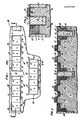
- FIG. 1 there is shown in top view a portion of a portion of a DRAM memory array having one transistor, one capacitor cells constructed according to the invention.
- Three “islands” referred to by numerals 92, 94 and 96 are located in a "sea" of polysilicon denoted by the numeral 112, each island being surrounded by a layer of silicon oxide 111.
- the invention is addressed at forming compact capacitors resistant to pinhole shorts and excessive discharge.
- the particular circuit elements located on each island are a pair of transistors 102 and 104 sharing a common drain 106 and each having a separate source 105.
- Each source is connected to a capacitor 117 having a first plate 114 formed vertically into the substrate and a ground plate which is formed by polysilicon 112.
- Drain 106 will be connected to a metal column line that is omitted from the drawing for clarity, as is the row line that applies voltage to one or more memory cells. Conventionally, a row line will enable all the cells on the row, one or more of which will be accessed for data and all of which will be refreshed. Connections to the transistors and a layered oxide 111 over sources 105 are omitted to provide greater clarity in the drawing.
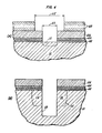
- FIG. 2 there is shown a cross section through line 2-2 of Fig. 1.
- This cross section extends through islands 92 and 94, separated by a trench 120 in the center of the drawing.
- the same two transistors 102 and 104 in each island formed in substrate 101 are shown with capacitor plates 114 on either side of trench 120.
- Trench 120 is lined with oxide 111 which also extends over source 105 and the top of capacitor plate 114.
- Trench 120 is filled with polysilicon 112 which is heavily doped, as is indicated by the P++ symbol.
- the polysilicon is protected by a field oxide 115.
- Two capacitors, referred to by the general numeral 117 are formed, sharing polysilicon 112 as a common ground plate and having oxide insulation 111 on either side of polysilicon 112.
- the two inner plates 114 complete the structure of capacitors 117. Plates 114 are electrically connected by common doping to sources 105.
- a further element in the cross section comprising a doped region having the same polarity as the doping in trench 120 and surrounding trench 120, not only in the plane shown in the cross section but on the surface of the "sea" of polysilicon extending around and facing each island that is above and below the plane of Fig. 2.
- Doped area 121 is not shown as extending into plates 114 of capacitors 117 because the amount of doping is insufficient to change the type of impurity of plates 114.
- the concentration at the edge of oxide 111 is merely reduced slightly.
- FIG. 3 Another side view of the array of islands shown in Fig. 1, looking along line 3-3 in Fig.1, is shown in Fig. 3.
- the section is taken through one of plates 114 in island 96 and through gate 103 of island 94, showing the bottom of source 105, the plate 114 itself, the oxide 111 that is formed on either side of islands 94 and 96 and extends down into the trench.
- region 121 is shown as extending only up to capacitor plate 114 in island 96, but extends up to gate oxide 109 in island 94.
- This region 121 serves an equivalent function to a conventional field implant by raising the threshold of formation of parasitic channels. These channels can form between islands or along the surface of oxide 111 that faces the island.
- a channel could be formed on the vertical surface of oxide 111 that is underneath the gate source and drain, of a transistor thus effectively short-circuiting not only the transistor, but also plate 114 to drain 106.
- the field implant suppresses the formation of parasitic channels. It has been a drawback of trench isolation methods in the prior art that there has been no effective way to provide the same suppression of the parasitic channels, and this is one of the problems that the present invention solves.
- the concentration of doped region 121 is indicated by P indicating a light concentration of approximately 5 x 10¹⁶ ions per cc, near the vertical silicon surface in the substrate 101 outside the N+ areas, which is formed by diffusion of the heavily doped impurities within polysilicon 112 through oxide 111 and into substrate 101 surrounding the trench. It is necessary, of course, that the impurity used in trench 112 be capable of diffusing through thin oxide. Boron has that property and is a material well known in the art.
- FIGs. 4a and 4b illustrate steps in the formation of a capacitor according to the invention in which an aperture having a width indicated by the arrow labeled 410, penetrates a series of layers comprising oxide layer 402 having an illustrative thickness of 500 angstroms, nitride layer 404 having an illustrative thickness of 1000 angstroms, and an oxide layer 406 having an illustrative thickness of 5000 angstroms.
- a further photoresist layer 408 having an aperture indicated by the arrow labeled 412 is placed above oxide layer 406 in order to define an ion implant area.
- Aperture 412 is made oversized in order to provide for alignment tolerance.
- a dose of phosphorus is implanted through aperture 410 in the region indicated by the numeral 113 with an illustrative concentration of 1015/centimeter2.
- Aperture 410 may be formed by any convenient means known in the art, such as by reactive ion etching (RIE).
- RIE reactive ion etching
- Fig. 4b the results of a diffusion drive at a temperature of between 1,100 and 1,150 degrees centigrade for several hours has expanded area 113 into area 113' having a nominal width of 2.1 microns and a nominal depth of 2.5 microns.
- This area 113' which will become plates 114 of capacitor 117, is shown as being penetrated by trench 120 which is formed by a second step of reactive ion etching to a depth of between 3 and 3.5 microns.
- this second RIE step part of oxide layer 406 is consumed.
- the thickness of layer 406 should, of course, be taken together with the properties of the particular RIE process being used so that the nitrid
- trench 120 After trench 120 is cut, there are further steps of growing a layer of oxide on the interior surface of trench 120 to a nominal thickness of approximately 400 angstroms; stripping the oxide by a conventional wet etch proces and growing a final layer of oxide to a nominal thickness of 100 angstroms.
- the trench is then filled by doped polycrystalline silicon formed in a standard process using, for example SiH4 together with B2H6 at standard temperatures and pressures well known to those skilled in the art.
- concentration of boron dopant in the polycrystalline silicon should be about 5x10¹⁸ per cc.
- the doped polycrystalline layer has been deposited throughout the trench region, the portion of the polycrystalline silicon lying above the islands is etched away, as is the remainder of oxide layer 406.
- a field oxide region is then grown over polycrystalline silicon 112 to protect the trench and the remainder of the circuit elements on the island are formed in a conventional manner.
- the doped polysilicon 112 in trench 120 is at the same potential as substrate 101, illustratively ground.
- substrate 101 illustratively ground.
- debris could easily cause short circuits or diodes that could discharge capacitor 117 or otherwise interfere with the circuit.
- any debris With the trench filling material of the same polarity and at the same potential as the substrate, any debris will be innocuous.
- capacitor 117 With a capacitor 117 is formed as shown in Fig. 2, there will be more stress on oxide 111, for a given oxide thickness, when polysilicon 112 is grounded than if it were at Vcc/2, but maintaining capacitor plate 112 at some intermediate voltage would risk shorts to the substrate 101.
- a further advantageous feature of the invention is that, with polysilicon 112 doped with P-type material and plate 114 and transistor source 105 and drain 106, doped with N-type material, the effect of a pinhole or other defect in oxide 111 is reduced. It is well known that thinner oxides have more holes than thick ones and that the result of a hole is usually a short circuit that ruins the chip. For example, when a conventional five volt level is being stored in a memory cell, the bit line 106, source 105 and capacitor plate 114 of that cell will all be raised to five volts. If there is a pinhole through oxide 111 with this invention, the N+ region will be at plus five volts and the P++ region will be at ground.
- the region of plate 114around the pinhole will be a P-N diode, reverse-baised at five volts, that will not conduct current. Short circuits through oxide 111 are thus "self-healing", resulting in greater yield than would be the case if a different combination of materials were used.
- the invention has been illustrated in the context of a conventional N-channel process and a DRAM memory cell. Those skilled in the art will readily be able to apply the principles of this invention to form capacitors in other circuits beside DRAMs, and to other combinations of voltage levels and doping materials.
Landscapes
- Engineering & Computer Science (AREA)
- Manufacturing & Machinery (AREA)
- Semiconductor Memories (AREA)
- Semiconductor Integrated Circuits (AREA)
Abstract
Description
- The field of the invention is the fabrication of vertical capacitors formed in the wall of a trench extending into a substrate.
- The use of trench capacitors for saving space in integrated circuits has been studied for some years. A convenient summary is an article by K. Minegishi et al. entitled "A Submicron CMOS Megabit Level Dynamic RAM Technology Using Doped Face Trench Capacitor Cell", IEDM '83.
- The invention relates to an improved integrated circuit fabrication process for trench capacitor formation in which the bottom of the trench receives an effective field implant to prevent discharge of the capacitor, by diffusion of an impurity through an oxide coating lining the walls of the trench and in which the capacitor formed has the property of resisting short circuits through pinholes in the insulation.
- A feature of the invention is the use of the improved capacitor in a compact one-transistor, one-capacitor memory cell.
-
- Fig. 1 illustrates a top view of portion of an integrated circuit containing capacitors constructed according to the invention.
- Fig. 2 illustrates a cross section of one embodiment of the invention.
- Fig. 3 illustrates a cross section of a different view of the elements shown in Fig. 1.
- Figs. 4a and 4b illustrate intermediate steps in the fabrication of a capacitor according to the invention.
- The art has long sought a practical method of saving space in DRAMs and other integrated circuits that employ capacitors by orienting the capacitors vertically. There have been considerable practical difficulties blocking the implementation of this approach, including problems associated with yield that are related to short circuits through what is necessarily a thin and relatively irregular insulating oxide insulation and also to problems associated with capacitor discharge through parasitic channels formed within the substrate (not necessaily at the surface) that tend to discharge trench capacitors. This invention is directed at an improved method of forming trench capacitors that reduces the aforementioned problems.
- Referring now to Fig. 1, there is shown in top view a portion of a portion of a DRAM memory array having one transistor, one capacitor cells constructed according to the invention. Three "islands" referred to by
numerals numeral 112, each island being surrounded by a layer of silicon oxide 111. The invention is addressed at forming compact capacitors resistant to pinhole shorts and excessive discharge. The particular circuit elements located on each island are a pair oftransistors common drain 106 and each having aseparate source 105. Each source is connected to acapacitor 117 having afirst plate 114 formed vertically into the substrate and a ground plate which is formed bypolysilicon 112.Drain 106 will be connected to a metal column line that is omitted from the drawing for clarity, as is the row line that applies voltage to one or more memory cells. Conventionally, a row line will enable all the cells on the row, one or more of which will be accessed for data and all of which will be refreshed. Connections to the transistors and a layered oxide 111 oversources 105 are omitted to provide greater clarity in the drawing. - Referring now to Fig. 2, there is shown a cross section through line 2-2 of Fig. 1. This cross section extends through
islands trench 120 in the center of the drawing. The same twotransistors substrate 101 are shown withcapacitor plates 114 on either side oftrench 120. Trench 120 is lined with oxide 111 which also extends oversource 105 and the top ofcapacitor plate 114.Trench 120 is filled withpolysilicon 112 which is heavily doped, as is indicated by the P⁺⁺ symbol. The polysilicon is protected by afield oxide 115. Two capacitors, referred to by thegeneral numeral 117, are formed, sharingpolysilicon 112 as a common ground plate and having oxide insulation 111 on either side ofpolysilicon 112. The twoinner plates 114 complete the structure ofcapacitors 117.Plates 114 are electrically connected by common doping tosources 105. - There is a further element in the cross section, indicated by the
numeral 121, comprising a doped region having the same polarity as the doping intrench 120 and surroundingtrench 120, not only in the plane shown in the cross section but on the surface of the "sea" of polysilicon extending around and facing each island that is above and below the plane of Fig. 2.Doped area 121 is not shown as extending intoplates 114 ofcapacitors 117 because the amount of doping is insufficient to change the type of impurity ofplates 114. The concentration at the edge of oxide 111 is merely reduced slightly. - Another side view of the array of islands shown in Fig. 1, looking along line 3-3 in Fig.1, is shown in Fig. 3. There, the section is taken through one of
plates 114 inisland 96 and throughgate 103 ofisland 94, showing the bottom ofsource 105, theplate 114 itself, the oxide 111 that is formed on either side ofislands region 121 is shown as extending only up tocapacitor plate 114 inisland 96, but extends up to gate oxide 109 inisland 94. Thisregion 121 serves an equivalent function to a conventional field implant by raising the threshold of formation of parasitic channels. These channels can form between islands or along the surface of oxide 111 that faces the island. In particular, a channel could be formed on the vertical surface of oxide 111 that is underneath the gate source and drain, of a transistor thus effectively short-circuiting not only the transistor, but alsoplate 114 to drain 106. In planar circuits, the field implant suppresses the formation of parasitic channels. It has been a drawback of trench isolation methods in the prior art that there has been no effective way to provide the same suppression of the parasitic channels, and this is one of the problems that the present invention solves. The concentration ofdoped region 121 is indicated by P indicating a light concentration of approximately 5 x 10¹⁶ ions per cc, near the vertical silicon surface in thesubstrate 101 outside the N⁺ areas, which is formed by diffusion of the heavily doped impurities withinpolysilicon 112 through oxide 111 and intosubstrate 101 surrounding the trench. It is necessary, of course, that the impurity used intrench 112 be capable of diffusing through thin oxide. Boron has that property and is a material well known in the art. - Further details of the process steps can be seen in Figs. 4a and 4b. Figs. 4a and 4b illustrate steps in the formation of a capacitor according to the invention in which an aperture having a width indicated by the arrow labeled 410, penetrates a series of layers comprising
oxide layer 402 having an illustrative thickness of 500 angstroms,nitride layer 404 having an illustrative thickness of 1000 angstroms, and anoxide layer 406 having an illustrative thickness of 5000 angstroms. A furtherphotoresist layer 408 having an aperture indicated by the arrow labeled 412 is placed aboveoxide layer 406 in order to define an ion implant area. Aperture 412 is made oversized in order to provide for alignment tolerance. A dose of phosphorus is implanted throughaperture 410 in the region indicated by thenumeral 113 with an illustrative concentration of 10¹⁵/centimeter².Aperture 410 may be formed by any convenient means known in the art, such as by reactive ion etching (RIE). In Fig. 4b, the results of a diffusion drive at a temperature of between 1,100 and 1,150 degrees centigrade for several hours has expandedarea 113 into area 113' having a nominal width of 2.1 microns and a nominal depth of 2.5 microns. This area 113', which will becomeplates 114 ofcapacitor 117, is shown as being penetrated bytrench 120 which is formed by a second step of reactive ion etching to a depth of between 3 and 3.5 microns. In the course of this second RIE step, part ofoxide layer 406 is consumed. The thickness oflayer 406 should, of course, be taken together with the properties of the particular RIE process being used so that thenitride layer 404 is protected during this step. - After
trench 120 is cut, there are further steps of growing a layer of oxide on the interior surface oftrench 120 to a nominal thickness of approximately 400 angstroms; stripping the oxide by a conventional wet etch proces and growing a final layer of oxide to a nominal thickness of 100 angstroms. - The trench is then filled by doped polycrystalline silicon formed in a standard process using, for example SiH₄ together with B₂H₆ at standard temperatures and pressures well known to those skilled in the art. The concentration of boron dopant in the polycrystalline silicon should be about 5x10¹⁸ per cc. In filling such a deep, narrow trench, there may well develop voids 116 within
polysilicon 112. That is no problem in this invention because the only requirement forpolysilicon 112 is that it form a conductive layer in the region ofcapacitor 117 and have a sufficient amount of polycrystalline silicon in the bottom of the trench to drive a sufficient quantity of boron in to form dopedlayer 121. This amount is non-critical, an advantageous feature of this invention. - After the doped polycrystalline layer has been deposited throughout the trench region, the portion of the polycrystalline silicon lying above the islands is etched away, as is the remainder of
oxide layer 406. A field oxide region is then grown overpolycrystalline silicon 112 to protect the trench and the remainder of the circuit elements on the island are formed in a conventional manner. - It is an advantageous feature of the invention that the doped
polysilicon 112 intrench 120 is at the same potential assubstrate 101, illustratively ground. There will often be small amounts of debris left from previous processing steps in the bottom oftrench 120, which must have a small width to depth ratio in order to occupy as little room as possible. The debris could easily cause short circuits or diodes that could dischargecapacitor 117 or otherwise interfere with the circuit. With the trench filling material of the same polarity and at the same potential as the substrate, any debris will be innocuous. - With a
capacitor 117 is formed as shown in Fig. 2, there will be more stress on oxide 111, for a given oxide thickness, whenpolysilicon 112 is grounded than if it were at Vcc/2, but maintainingcapacitor plate 112 at some intermediate voltage would risk shorts to thesubstrate 101. - A further advantageous feature of the invention is that, with
polysilicon 112 doped with P-type material andplate 114 andtransistor source 105 and drain 106, doped with N-type material, the effect of a pinhole or other defect in oxide 111 is reduced. It is well known that thinner oxides have more holes than thick ones and that the result of a hole is usually a short circuit that ruins the chip. For example, when a conventional five volt level is being stored in a memory cell, thebit line 106,source 105 andcapacitor plate 114 of that cell will all be raised to five volts. If there is a pinhole through oxide 111 with this invention, the N+ region will be at plus five volts and the P⁺⁺ region will be at ground. The region of plate 114around the pinhole will be a P-N diode, reverse-baised at five volts, that will not conduct current. Short circuits through oxide 111 are thus "self-healing", resulting in greater yield than would be the case if a different combination of materials were used. - With this invention, the problems of parasitic channel discharge and of pinhole shorts are overcome, together with the avoidance of potential problems that might be caused by imperfect cleaning of the bottom of the trench.
- The invention has been illustrated in the context of a conventional N-channel process and a DRAM memory cell. Those skilled in the art will readily be able to apply the principles of this invention to form capacitors in other circuits beside DRAMs, and to other combinations of voltage levels and doping materials.
Claims (7)
forming a protective layer on said substrate;
cutting an implant aperture having first and second aperture dimensions along first and second axes in said substrate, in a predetermined location in said substrate dimensions along said first and second axes, through said protective layer to said substrate;
implanting a predetermined dose of ions of conductivity type opposite to said substrate conductivity type;
diffusing said dose of ions into said substrate by heating said substrate to a predetermined temperature for a predetermined time such that a substantial concentration of said ions of said opposite conductivity type extends a predetermined distance from said implant aperture, whereby that portion of said dose of ions extending in said substrate below said predetermined capacitor plate location forms a plate conductive region extending downwardly into said substrate along a third axis and having first, second and third plate dimensions along said first, second and third axes;
cutting a trench into said substrate through said implant aperture, thereby forming a trench wall on that surface of said trench extending into said substrate through said plate conductive region with a wall area having a wall length greater than said first plate dimension along said first axis and a wall depth greater than said third plate dimension along said third axis;
growing a wall layer of silicon dioxide on said trench wall adjacent said plate conductive region and extending along said trench wall beyond said plate conductive region;
filling said trench with polycrystalline silicon filler heavily doped with a trench dopant material of the same conductivity type as said substrate conductivity type and having the capacity of diffusing through thin layers of silicon dioxide; and
heating said substrate to predetermined temperature for a predetermined time sufficient to diffuse a predetermined quantity of said trench dopant material through said wall layer of silicon dioxide to form a diffused channel stop region disposed about said plate conductive region in that portion of said silicon substrate abutting said trench wall and outside and first and third plate dimensions, whereby a parallel-plate capacitor is formed, one plate of which consists of said conductive plate region and the other plate of which is formed by said heavily doped polycrystalline filler, which capcitor has improved resistance to discharge through the effect of said diffused channel stop region.
said vertical capacitor comprises a first conductive plate, doped with an N-type dopant, extending downwardly into a silicon semiconductor substrate and positioned in an edge of a trench cut into said substrate,
an insulating layer of silicon dioxide formed on the surface of said trench and extending over said first conductive plate;
a second conductive plate extending over the past said first conductive plate and being formed from polycrystalline silicon doped with a P-type dopant capable of diffusing through a thin layer of silicon dioxide;
a diffused layer of said P-type dopant extending in said substrate about said first conductive plate and adjacent to said surface; and
means for connecting said second conductive plate to ground.
Priority Applications (1)
| Application Number | Priority Date | Filing Date | Title |
|---|---|---|---|
| AT86402222T ATE91569T1 (en) | 1985-10-07 | 1986-10-07 | GROOVED CAPACITOR AND DRAM CELL. |
Applications Claiming Priority (2)
| Application Number | Priority Date | Filing Date | Title |
|---|---|---|---|
| US785195 | 1985-10-07 | ||
| US06/785,195 US4679300A (en) | 1985-10-07 | 1985-10-07 | Method of making a trench capacitor and dram memory cell |
Publications (3)
| Publication Number | Publication Date |
|---|---|
| EP0220109A2 true EP0220109A2 (en) | 1987-04-29 |
| EP0220109A3 EP0220109A3 (en) | 1989-05-31 |
| EP0220109B1 EP0220109B1 (en) | 1993-07-14 |
Family
ID=25134727
Family Applications (1)
| Application Number | Title | Priority Date | Filing Date |
|---|---|---|---|
| EP86402222A Expired - Lifetime EP0220109B1 (en) | 1985-10-07 | 1986-10-07 | Improved trench capacitor and dram memory cell |
Country Status (6)
| Country | Link |
|---|---|
| US (1) | US4679300A (en) |
| EP (1) | EP0220109B1 (en) |
| JP (1) | JPH0810754B2 (en) |
| KR (1) | KR950008791B1 (en) |
| AT (1) | ATE91569T1 (en) |
| DE (1) | DE3688694T2 (en) |
Cited By (1)
| Publication number | Priority date | Publication date | Assignee | Title |
|---|---|---|---|---|
| GB2238909A (en) * | 1989-12-08 | 1991-06-12 | Samsung Electronics Co Ltd | Capacitors for DRAM cells |
Families Citing this family (15)
| Publication number | Priority date | Publication date | Assignee | Title |
|---|---|---|---|---|
| US5227316A (en) * | 1985-01-22 | 1993-07-13 | National Semiconductor Corporation | Method of forming self aligned extended base contact for a bipolar transistor having reduced cell size |
| US5045916A (en) * | 1985-01-22 | 1991-09-03 | Fairchild Semiconductor Corporation | Extended silicide and external contact technology |
| US5061986A (en) * | 1985-01-22 | 1991-10-29 | National Semiconductor Corporation | Self-aligned extended base contact for a bipolar transistor having reduced cell size and improved electrical characteristics |
| US4737829A (en) * | 1985-03-28 | 1988-04-12 | Nec Corporation | Dynamic random access memory device having a plurality of one-transistor type memory cells |
| JPH0682800B2 (en) * | 1985-04-16 | 1994-10-19 | 株式会社東芝 | Semiconductor memory device |
| US5082795A (en) * | 1986-12-05 | 1992-01-21 | General Electric Company | Method of fabricating a field effect semiconductor device having a self-aligned structure |
| JP2523712B2 (en) * | 1987-11-25 | 1996-08-14 | 松下電器産業株式会社 | Plasma doping method |
| US5021852A (en) * | 1989-05-18 | 1991-06-04 | Texas Instruments Incorporated | Semiconductor integrated circuit device |
| WO1992005896A1 (en) * | 1990-10-02 | 1992-04-16 | University Of Houston System | Method and apparatus for doping silicon wafers using a solid dopant source and rapid thermal processing |
| US5550082A (en) * | 1993-11-18 | 1996-08-27 | The University Of Houston System | Method and apparatus for doping silicon wafers using a solid dopant source and rapid thermal processing |
| US6057195A (en) * | 1998-05-22 | 2000-05-02 | Texas Instruments - Acer Incorporated | Method of fabricating high density flat cell mask ROM |
| US6489646B1 (en) * | 2002-01-23 | 2002-12-03 | Winbond Electronics Corporation | DRAM cells with buried trench capacitors |
| US7608927B2 (en) * | 2002-08-29 | 2009-10-27 | Micron Technology, Inc. | Localized biasing for silicon on insulator structures |
| US7633110B2 (en) * | 2004-09-21 | 2009-12-15 | Taiwan Semiconductor Manufacturing Co., Ltd. | Memory cell |
| US10453754B1 (en) | 2018-06-28 | 2019-10-22 | Globalfoundries Inc. | Diffused contact extension dopants in a transistor device |
Family Cites Families (8)
| Publication number | Priority date | Publication date | Assignee | Title |
|---|---|---|---|---|
| NL7710635A (en) * | 1977-09-29 | 1979-04-02 | Philips Nv | METHOD OF MANUFACTURING A SEMICONDUCTOR DEVICE. |
| JPS5681974A (en) * | 1979-12-07 | 1981-07-04 | Toshiba Corp | Manufacture of mos type semiconductor device |
| US4353086A (en) * | 1980-05-07 | 1982-10-05 | Bell Telephone Laboratories, Incorporated | Silicon integrated circuits |
| US4397075A (en) * | 1980-07-03 | 1983-08-09 | International Business Machines Corporation | FET Memory cell structure and process |
| JPS583269A (en) * | 1981-06-30 | 1983-01-10 | Fujitsu Ltd | Vertical type mos dynamic memory cell |
| JPS58137245A (en) * | 1982-02-10 | 1983-08-15 | Hitachi Ltd | Semiconductor memory and its manufacture |
| JPS60126861A (en) * | 1983-12-13 | 1985-07-06 | Fujitsu Ltd | Semiconductor memory device |
| US4604150A (en) * | 1985-01-25 | 1986-08-05 | At&T Bell Laboratories | Controlled boron doping of silicon |
-
1985
- 1985-10-07 US US06/785,195 patent/US4679300A/en not_active Expired - Lifetime
-
1986
- 1986-10-07 EP EP86402222A patent/EP0220109B1/en not_active Expired - Lifetime
- 1986-10-07 JP JP61238993A patent/JPH0810754B2/en not_active Expired - Fee Related
- 1986-10-07 DE DE86402222T patent/DE3688694T2/en not_active Expired - Fee Related
- 1986-10-07 KR KR1019860008393A patent/KR950008791B1/en not_active Expired - Fee Related
- 1986-10-07 AT AT86402222T patent/ATE91569T1/en not_active IP Right Cessation
Cited By (1)
| Publication number | Priority date | Publication date | Assignee | Title |
|---|---|---|---|---|
| GB2238909A (en) * | 1989-12-08 | 1991-06-12 | Samsung Electronics Co Ltd | Capacitors for DRAM cells |
Also Published As
| Publication number | Publication date |
|---|---|
| US4679300A (en) | 1987-07-14 |
| KR870004516A (en) | 1987-05-11 |
| EP0220109B1 (en) | 1993-07-14 |
| DE3688694D1 (en) | 1993-08-19 |
| DE3688694T2 (en) | 1994-01-20 |
| JPH0810754B2 (en) | 1996-01-31 |
| JPS62163365A (en) | 1987-07-20 |
| KR950008791B1 (en) | 1995-08-08 |
| EP0220109A3 (en) | 1989-05-31 |
| ATE91569T1 (en) | 1993-07-15 |
Similar Documents
| Publication | Publication Date | Title |
|---|---|---|
| US5618745A (en) | Method of manufacturing a one transistor one-capacitor memory cell structure with a trench containing a conductor penetrating a buried insulating film | |
| US6222217B1 (en) | Semiconductor device and manufacturing method thereof | |
| US4922313A (en) | Process for manufacturing semiconductor memory device and product formed thereby | |
| KR100338462B1 (en) | Device manufacturing method comprising self-amplifying dynamic MOS transistor memory cells | |
| US6150210A (en) | Memory cell that includes a vertical transistor and a trench capacitor | |
| US5316962A (en) | Method of producing a semiconductor device having trench capacitors and vertical switching transistors | |
| US5103276A (en) | High performance composed pillar dram cell | |
| US4792834A (en) | Semiconductor memory device with buried layer under groove capacitor | |
| US5376814A (en) | Method of constructing reduced size highly integrated static random access memory with double vertical channel structure | |
| JP5629872B2 (en) | SOI type transistor | |
| US5398205A (en) | Semiconductor memory device having trench in which word line is buried | |
| EP0220109B1 (en) | Improved trench capacitor and dram memory cell | |
| US4864375A (en) | Dram cell and method | |
| US5181089A (en) | Semiconductor memory device and a method for producing the same | |
| US6437401B1 (en) | Structure and method for improved isolation in trench storage cells | |
| US4791463A (en) | Structure for contacting devices in three dimensional circuitry | |
| US4914739A (en) | Structure for contacting devices in three dimensional circuitry | |
| EP0713253A1 (en) | Trench capacitor DRAM cell | |
| EP0462576B1 (en) | DRAM using barrier layer | |
| US4987470A (en) | Semiconductor dram device having a trench | |
| JPH0612805B2 (en) | Method of manufacturing semiconductor memory device | |
| JPS61108163A (en) | Semiconductor memory device and manufacture thereof | |
| EP0266572B1 (en) | Semiconductor memory device having a plurality of memory cells of single transistor type | |
| JPH0680805B2 (en) | MIS type semiconductor memory device | |
| US5248891A (en) | High integration semiconductor device |
Legal Events
| Date | Code | Title | Description |
|---|---|---|---|
| PUAI | Public reference made under article 153(3) epc to a published international application that has entered the european phase |
Free format text: ORIGINAL CODE: 0009012 |
|
| AK | Designated contracting states |
Kind code of ref document: A2 Designated state(s): AT DE FR GB IT NL |
|
| PUAL | Search report despatched |
Free format text: ORIGINAL CODE: 0009013 |
|
| AK | Designated contracting states |
Kind code of ref document: A3 Designated state(s): AT DE FR GB IT NL |
|
| 17P | Request for examination filed |
Effective date: 19890801 |
|
| 17Q | First examination report despatched |
Effective date: 19910911 |
|
| RAP1 | Party data changed (applicant data changed or rights of an application transferred) |
Owner name: SGS-THOMSON MICROELECTRONICS, INC. (A DELAWARE COR |
|
| GRAA | (expected) grant |
Free format text: ORIGINAL CODE: 0009210 |
|
| AK | Designated contracting states |
Kind code of ref document: B1 Designated state(s): AT DE FR GB IT NL |
|
| PG25 | Lapsed in a contracting state [announced via postgrant information from national office to epo] |
Ref country code: NL Effective date: 19930714 Ref country code: AT Effective date: 19930714 |
|
| REF | Corresponds to: |
Ref document number: 91569 Country of ref document: AT Date of ref document: 19930715 Kind code of ref document: T |
|
| ITF | It: translation for a ep patent filed | ||
| REF | Corresponds to: |
Ref document number: 3688694 Country of ref document: DE Date of ref document: 19930819 |
|
| ET | Fr: translation filed | ||
| NLV1 | Nl: lapsed or annulled due to failure to fulfill the requirements of art. 29p and 29m of the patents act | ||
| PLBE | No opposition filed within time limit |
Free format text: ORIGINAL CODE: 0009261 |
|
| STAA | Information on the status of an ep patent application or granted ep patent |
Free format text: STATUS: NO OPPOSITION FILED WITHIN TIME LIMIT |
|
| 26N | No opposition filed | ||
| REG | Reference to a national code |
Ref country code: GB Ref legal event code: 732E |
|
| REG | Reference to a national code |
Ref country code: FR Ref legal event code: TP |
|
| PGFP | Annual fee paid to national office [announced via postgrant information from national office to epo] |
Ref country code: DE Payment date: 19971010 Year of fee payment: 12 |
|
| PG25 | Lapsed in a contracting state [announced via postgrant information from national office to epo] |
Ref country code: DE Free format text: LAPSE BECAUSE OF NON-PAYMENT OF DUE FEES Effective date: 19990803 |
|
| REG | Reference to a national code |
Ref country code: GB Ref legal event code: IF02 |
|
| PGFP | Annual fee paid to national office [announced via postgrant information from national office to epo] |
Ref country code: GB Payment date: 20031001 Year of fee payment: 18 |
|
| PGFP | Annual fee paid to national office [announced via postgrant information from national office to epo] |
Ref country code: FR Payment date: 20031003 Year of fee payment: 18 |
|
| PG25 | Lapsed in a contracting state [announced via postgrant information from national office to epo] |
Ref country code: GB Free format text: LAPSE BECAUSE OF NON-PAYMENT OF DUE FEES Effective date: 20041007 |
|
| GBPC | Gb: european patent ceased through non-payment of renewal fee |
Effective date: 20041007 |
|
| PG25 | Lapsed in a contracting state [announced via postgrant information from national office to epo] |
Ref country code: FR Free format text: LAPSE BECAUSE OF NON-PAYMENT OF DUE FEES Effective date: 20050630 |
|
| REG | Reference to a national code |
Ref country code: FR Ref legal event code: ST |
|
| PG25 | Lapsed in a contracting state [announced via postgrant information from national office to epo] |
Ref country code: IT Free format text: LAPSE BECAUSE OF NON-PAYMENT OF DUE FEES;WARNING: LAPSES OF ITALIAN PATENTS WITH EFFECTIVE DATE BEFORE 2007 MAY HAVE OCCURRED AT ANY TIME BEFORE 2007. THE CORRECT EFFECTIVE DATE MAY BE DIFFERENT FROM THE ONE RECORDED. Effective date: 20051007 |